

Page 1
IRFB11N50A, SiHFB11N50A
*
Power MOSFET
Vishay Siliconix
PRODUCT SUMMARY
VDS (V) 500
R
(Ω)V
DS(on)
Q
(Max.) (nC) 52
g
Q
(nC) 13
gs
Q
(nC) 18
gd
Configuration Single
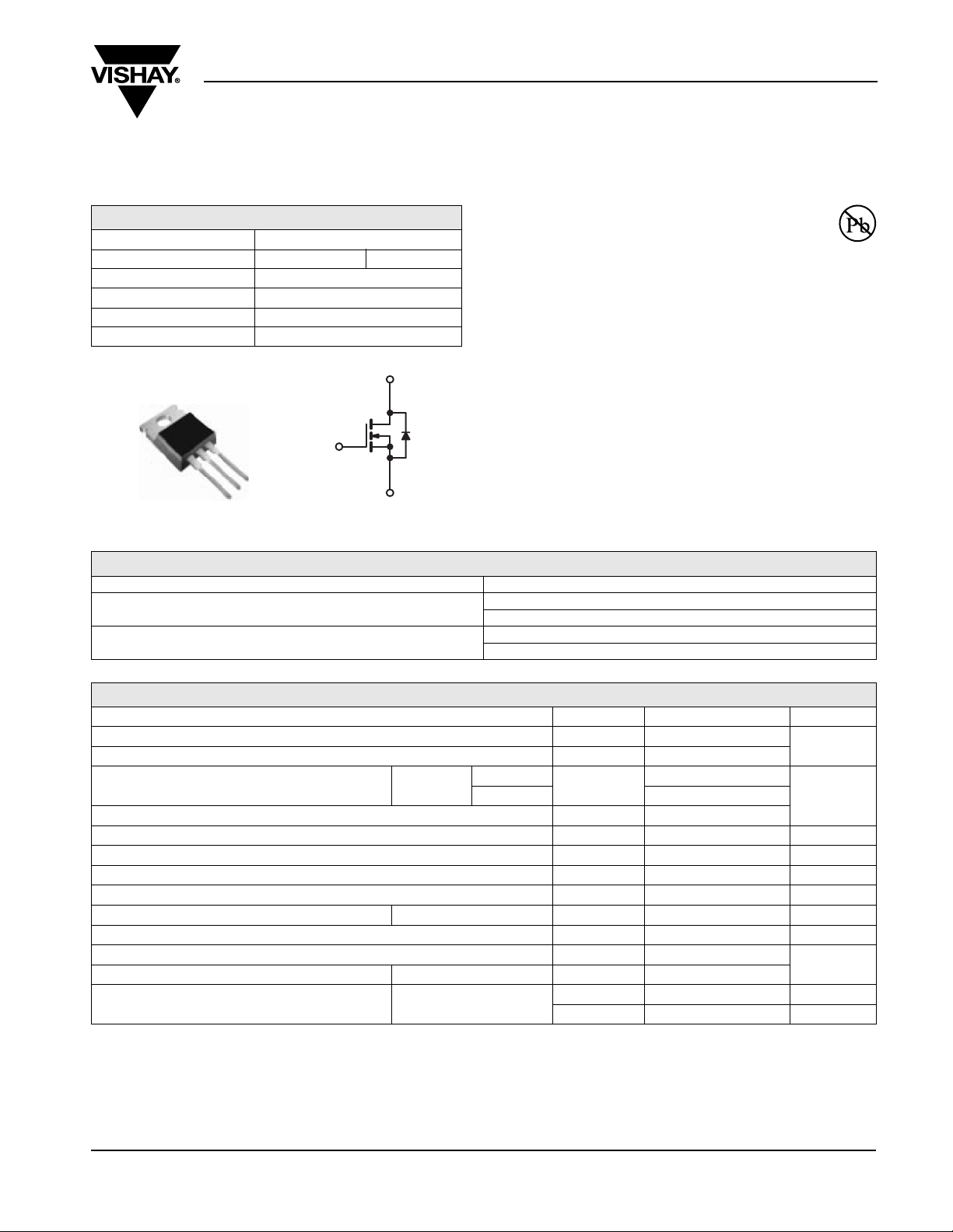
TO-220
= 10 V 0.52
GS
D
FEATURES
• Low Gate Charge Qg Results in Simple Drive
Requirement
• Improved Gate, Avalanche and Dynamic dV/dt
Ruggedness
• Fully Characterized Capacitance and
Avalanche Voltage and current
• Lead (Pb)-free Available
APPLICATIONS
• Switch Mode Power Supply (SMPS)
• Uninterruptible Power Supply
G
• High Speed Power Switching
APPLICABLE OFF LINE SMPS TOPOLOGIES
S
D
G
N-Channel MOSFET
S
• Two Transistor Forward
• Half and Full Bridge
• Power Factor Correction Boost
ORDERING INFORMATION
Package TO-220
Lead (Pb)-free
SnPb
IRFB11N50APbF
SiHFB11N50A-E3
IRFB11N50A
SiHFB11N50A
Available
RoHS
COMPLIANT
ABSOLUTE MAXIMUM RATINGS TC = 25 °C, unless otherwise noted
PARAMETER SYMBOL LIMIT UNIT
Drain-Source Voltage V
Gate-Source Voltage V
T
= 25 °C
Continuous Drain Current V
Pulsed Drain Current
a
at 10 V
GS
C
= 100 °C 7.0
C
DS
± 30
GS
I
D
IDM 44
Linear Derating Factor 1.3 W/°C
Single Pulse Avalanche Energy
Repetitive Avalanche Current
Repetitive Avalanche Energy
Maximum Power Dissipation T
Peak Diode Recovery dV/dt
b
a
a
= 25 °C P
c
C
Operating Junction and Storage Temperature Range T
E
AS
I
AR
E
AR
D
dV/dt 6.9 V/ns
, T
J
stg
Soldering Recommendations (Peak Temperature) for 10 s 300
Mounting Torque 6-32 or M3 screw
Notes
a. Repetitive rating; pulse width limited by maximum junction temperature (see fig. 11).
b. Starting T
c. I
SD
= 25 °C, L = 4.5 mH, RG = 25 Ω, IAS = 11 A (see fig. 12).
J
≤ 11 A, dI/dt ≤ 140 A/µs, VDD ≤ VDS, TJ ≤ 150 °C.
d. 1.6 mm from case.
* Pb containing terminations are not RoHS compliant, exemptions may apply
Document Number: 91094 www.vishay.com
S-81243-Rev. B, 21-Jul-08 1
500
11
275 mJ
11 A
17 mJ
170 W
- 55 to + 150
d
10 lbf · in
1.1 N · m
V
AT
°C
Page 2
IRFB11N50A, SiHFB11N50A
Vishay Siliconix
THERMAL RESISTANCE
PARAMETER SYMBOL TYP. MAX. UNIT
Maximum Junction-to-Ambient R
Maximum Junction-to-Case (Drain) R
thJA
thCS
thJC
SPECIFICATIONS TJ = 25 °C, unless otherwise noted
PARAMETER SYMBOL TEST CONDITIONS MIN. TYP. MAX. UNIT
Static
Drain-Source Breakdown Voltage V
Gate-Source Threshold Voltage V
Gate-Source Leakage I
Zero Gate Voltage Drain Current I
Drain-Source On-State Resistance R
Forward Transconductance g
Dynamic
Input Capacitance C
Output Capacitance C
Reverse Transfer Capacitance C
Output Capacitance C
Effective Output Capacitance C
Total Gate Charge Q
Gate-Drain Charge Q
Turn-On Delay Time t
Rise Time t
Turn-Off Delay Time t
Fall Time t
Drain-Source Body Diode Characteristics
Continuous Source-Drain Diode Current I
Pulsed Diode Forward Current
a
Body Diode Voltage V
Body Diode Reverse Recovery Time t
Body Diode Reverse Recovery Charge Q
Forward Turn-On Time t
Notes
a. Repetitive rating; pulse width limited by maximum junction temperature (see fig. 11).
b. Pulse width ≤ 300 µs; duty cycle ≤ 2 %.
c. C
effective is a fixed capacitance that gives the same charging time as C
oss
DS
GS(th)
V
GSS
DSS
VGS = 10 V ID = 6.6 A
DS(on)
fs
iss
- 208 -
oss
-8.1-
rss
oss
eff. VDS = 0 V to 400 V - 97 -
oss
g
--13
gs
--18
gd
d(on)
r
-32-
d(off)
-28-
f
S
I
SM
SD
rr
rr
on
V
V
GS
V
GS
MOSFET symbol
showing the
integral reverse
p - n junction diode
TJ = 25 °C, IF = 11 A, dI/dt = 100 A/µs
-62
0.50 -
°C/WCase-to-Sink, Flat, Greased Surface R
-0.75
VGS = 0 V, ID = 250 µA 500 - - V
VDS = VGS, ID = 250 µA 2.0 - 4.0 V
= ± 30 V - - ± 100 nA
GS
VDS = 500 V, VGS = 0 V - - 25
= 400 V, VGS = 0 V, TJ = 150 °C - - 250
DS
b
- - 0.52 Ω
VDS = 50 V, ID = 6.6 A 6.1 - - S
VGS = 0 V,
= 25 V,
V
DS
- 1423 -
f = 1.0 MHz, see fig. 5
V
= 1.0 V, f = 1.0 MHz - 2000 -
DS
= 0 V
= 400 V, f = 1.0 MHz - 55 -
V
DS
--52
= 11 A, VDS = 400 V
I
= 10 V
D
see fig. 6 and 13
b
-14-
V
= 250 V, ID = 11 A
DD
R
= 9.1 Ω, RD = 22 Ω, see fig. 10
G
G
TJ = 25 °C, IS = 11 A, VGS = 0 V
b
D
S
b
-35-
--11
--44
--1.5V
- 510 770 ns
b
-3.45.1µC
Intrinsic turn-on time is negligible (turn-on is dominated by LS and LD)
while VDS is rising from 0 to 80 % VDS.
oss
µA
pF
nC Gate-Source Charge Q
ns
A
www.vishay.com Document Number: 91094
2 S-81243-Rev. B, 21-Jul-08
Page 3
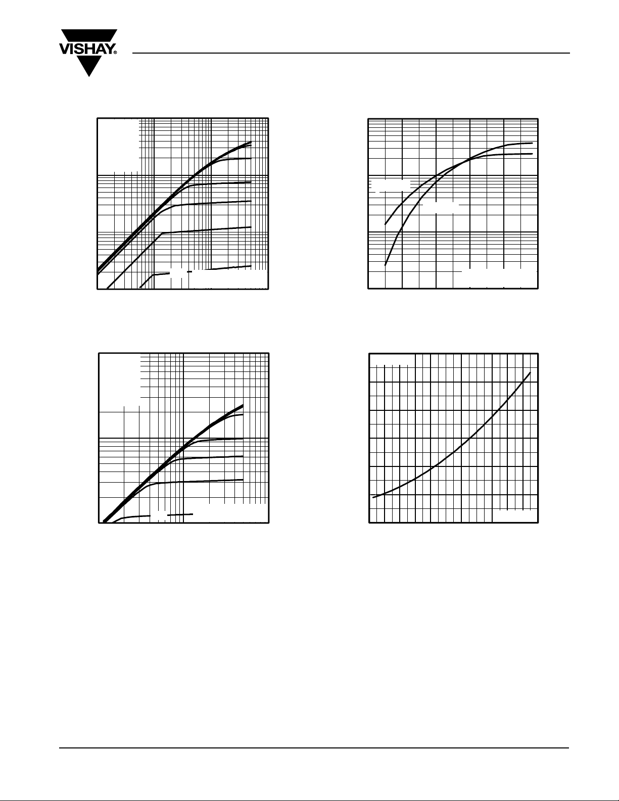
TYPICAL CHARACTERISTICS 25 °C, unless otherwise noted
100
10
TOP
BOTTOM
VGS
15V
10V
8.0V
7.0V
6.0V
5.5V
5.0V
4.5V
IRFB11N50A, SiHFB11N50A
Vishay Siliconix
100
10
°
T = 150 C
J
°
T = 25 C
J
1
D
I , Drain-to-Source Current (A)
4.5V
20µs PULSE WIDTH
°
T = 25 C
0.1
0.1 1 10 100
V , Drain-to-Source Voltage (V)
DS
J
Fig. 1 - Typical Output Characteristics
100
10
D
I , Drain-to-Source Current (A)
1
VGS
TOP
15V
10V
8.0V
7.0V
6.0V
5.5V
5.0V
BOTTOM
4.5V
4.5V
1 10 100
V , Drain-to-Source Volt age (V)
DS
20µs PULSE WIDTH
T = 150 C
°
J
Fig. 2 - Typical Output Characteristics
1
D
I , Drain-to-Source Current (A)
V = 50V
DS
0.1
4.0 5.0 6.0 7.0 8.0 9.0
V , Gate-to-Source Voltage (V)
GS
20µs PULSE WIDT H
Fig. 3 - Typical Transfer Characteristics
3.0
2.5
2.0
1.5
(Normalized)
1.0
0.5
DS(on)
R , Drain-to-Source On Resistance
0.0
11A
I =
D
V =
GS
-60 -40 -20 0 20 40 60 80 100 120 140 160
T , Junction Temperature ( C)
J
°
Fig. 4 - Normalized On-Resistance vs. Temperature
10V
Document Number: 91094 www.vishay.com
S-81243-Rev. B, 21-Jul-08 3
Page 4

IRFB11N50A, SiHFB11N50A
Vishay Siliconix
2400
2000
1600
1200
800
C, Capacitance (pF)
400
0
1 10 100 1000
V = 0V, f = 1MHz
GS
C = C + C , C SHORTED
iss gs gd ds
C = C
rss gd
C = C + C
oss ds gd
iss
oss
rss
V , Drain-to-Source Voltage (V)
DS
A
Fig. 5 - Typical Capacitance vs. Drain-to-Source Voltage
20
I =
6.6A
D
V = 400V
DS
V = 250V
16
DS
V = 100V
DS
100
10
°
T = 150 C
J
1
°
T = 25 C
J
SD
I , Reverse Drain Current (A)
V = 0 V
0.1
0.0 0.4 0.8 1.2 1.6
V ,Source-to-Drain Voltage (V)
SD
GS
Fig. 7 - Typical Source-Drain Diode Forward Voltage
1000
OPERATION IN THIS AREA LIMITED
100
BY R
DS(on)
12
8
4
GS
V , Gate-to-Source Voltage (V)
FOR TEST CIRCUIT
0
0 10 20 30 40 50
Q , Total Gate Charge (nC)
Fig. 6 - Typical Gate Charge vs. Gate-to-Source Voltage
G
SEE FIGURE
13
10us
10
D
I , Drain Current (A)I , Drain Current (A)
1
°
= 25 C
C
T T= 150 C
Single Pulse
0.1
10 100 1000 10000
°
J
V , Drain-to-Source Voltage (V)
DS
100us
1ms
10ms
Fig. 8 - Maximum Safe Operating Area
www.vishay.com Document Number: 91094
4 S-81243-Rev. B, 21-Jul-08
Page 5

IRFB11N50A, SiHFB11N50A
A
Vishay Siliconix
R
D.U.T.
D
+
V
DD
-
12
10
R
8
6
V
DS
V
GS
G
10V
Pulse Width ≤ 1 µs
Duty Factor ≤ 0.1 %
4
D
I , Drain Current (A)
2
0
25 50 75 100 125 150
T , Case Temperature ( C)
C
°
Fig. 9 - Maximum Drain Current vs. Case Temperature
1
D = 0.50
thJC
0.20
0.1
0.10
0.05
Thermal Response (Z )
0.01
0.02
0.01
0.00001 0.0001 0.001 0.01 0.1 1
SINGLE PULSE
(THERMAL RESPONSE)
t , Rectangular Pulse Duration (s)
1
Fig. 11 - Maximum Effective Transient Thermal Impedance, Junction-to-Case
Fig. 10a - Switching Time Test Circuit
V
DS
90 %
10 %
V
GS
t
d(on)tr
t
d(off)tf
Fig. 10b - Switching Time Waveforms
P
DM
t
1
Notes:
1. Duty factor D = t / t
2. Peak T = P x Z + T
1 2
J DM thJC C
t
2
V
DS
15 V
Driver
+
V
A
DD
-
R
V
G
20 V
DS
L
D.U.T.
I
AS
0.01
t
p
Ω
Fig. 12a - Unclamped Inductive Test Circuit
I
AS
Fig. 12b - Unclamped Inductive Waveforms
t
p
Document Number: 91094 www.vishay.com
S-81243-Rev. B, 21-Jul-08 5
Page 6

IRFB11N50A, SiHFB11N50A
A
Vishay Siliconix
600
500
TOP
BOTTOM
I
D
4.9A
7.0A
11A
400
300
200
100
AS
E , Single Pulse Avalanche Energy (mJ)
0
25 50 75 100 125 150
Starting T , Junction Temperature ( C)
J
°
Fig. 12c - Maximum Avalanche Energy vs. Drain Current
660
640
Q
G
10 V
Q
GS
V
G
Q
GD
Charge
Fig. 13a - Basic Gate Charge Waveform
Current regulator
Same type as D.U.T.
50 kΩ
12 V
0.2 µF
V
GS
0.3 µF
D.U.T.
3 mA
+
V
DS
-
620
600
DSav
V , Avalanche Voltage (V)
580
0.0 1.0 2.0 3.0 4.0 5.0 6.0 7.0
I , Avalanche Current (A)
av
Fig. 12d - Typical Drain-to-Source Voltage vs. Avalanche
Current
I
Current sampling resistors
G
I
D
Fig. 13b - Gate Charge Test Circuit
www.vishay.com Document Number: 91094
6 S-81243-Rev. B, 21-Jul-08
Page 7
IRFB11N50A, SiHFB11N50A
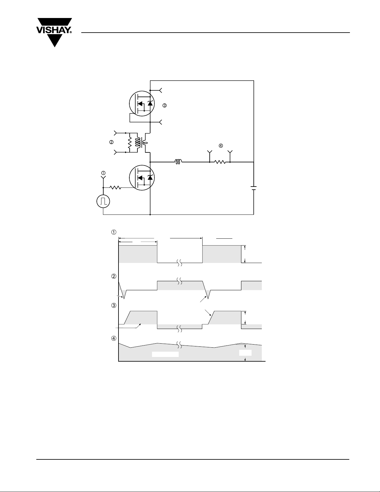
Peak Diode Recovery dV/dt Test Circuit
Vishay Siliconix
D.U.T
+
-
R
G
Driver gate drive
P.W.
+
Circuit layout considerations
• Low stray inductance
• Ground plane
• Low leakage inductance
current transformer
-
• dV/dt controlled by R
• Driver same type as D.U.T.
• I
controlled by duty factor "D"
SD
• D.U.T. - device under test
Period
-
D =
G
P. W.
Period
+
+
V
DD
-
= 10 V*
V
GS
waveform
SD
Body diode forward
current
waveform
DS
Body diode forward drop
Ripple ≤ 5 %
= 5 V for logic level devices
GS
Diode recovery
dV/dt
dI/dt
V
DD
I
SD
Reverse
recovery
current
Re-applied
voltage
D.U.T. I
D.U.T. V
Inductor current
* V
Fig. 14 - For N-Channel
Vishay Siliconix maintains worldwide manufacturing capability. Products may be manufactured at one of several qualified locations. Reliability data for Silicon
Technology and Package Reliability represent a composite of all qualified locations. For related documents such as package/tape drawings, part marking, and
reliability data, see http://www.vishay.com/ppg?91094.
Document Number: 91094 www.vishay.com
S-81243-Rev. B, 21-Jul-08 7
Page 8

Legal Disclaimer Notice
Vishay
Disclaimer
All product specifications and data are subject to change without notice.
Vishay Intertechnology, Inc., its affiliates, agents, and employees, and all persons acting on its or their behalf
(collectively, “Vishay”), disclaim any and all liability for any errors, inaccuracies or incompleteness contained herein
or in any other disclosure relating to any product.
Vishay disclaims any and all liability arising out of the use or application of any product described herein or of any
information provided herein to the maximum extent permitted by law. The product specifications do not expand or
otherwise modify Vishay’s terms and conditions of purchase, including but not limited to the warranty expressed
therein, which apply to these products.
No license, express or implied, by estoppel or otherwise, to any intellectual property rights is granted by this
document or by any conduct of Vishay.
The products shown herein are not designed for use in medical, life-saving, or life-sustaining applications unless
otherwise expressly indicated. Customers using or selling Vishay products not expressly indicated for use in such
applications do so entirely at their own risk and agree to fully indemnify Vishay for any damages arising or resulting
from such use or sale. Please contact authorized Vishay personnel to obtain written terms and conditions regarding
products designed for such applications.
Product names and markings noted herein may be trademarks of their respective owners.
Document Number: 91000 www.vishay.com
Revision: 18-Jul-08 1
 Loading...