

Page 1
SiE832DF
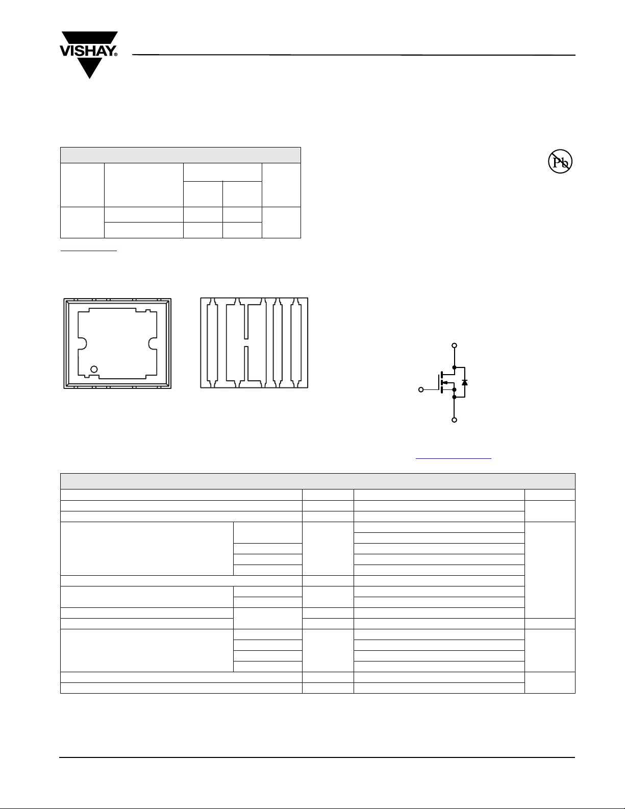
PRODUCT SUMMARY
VDS (V)
0.0055 at V
40
Package Drawing
http://www.vishay.com/doc?73398
0.007 at V
D
r
DS(on)
(Ω)
GS
GS
= 10 V
= 4.5 V
6 7 8 9 10
D S S G D
New Product
N-Channel 40-V (D-S) MOSFET
FEATURES
• TrenchFET® Power MOSFET
• Ultra Low Thermal Resistance Using
Top-Exposed PolarPAK
Double-Sided Cooling
• Leadframe-Based New Encapsulated Package
- Die Not Exposed
- Same Layout Regardless of Die Size
• Low Q
• 100 % R
gd/Qgs
g
APPLICATIONS
•VRM
• Point-of-Load
• Synchronous Rectification
Silicon
Limit
103
91
PolarPAK
a
(A)
I
D
Package
Limit
67 8 9
50
50
Qg (Typ)
25 nC
10
D D S G
Vishay Siliconix
®
Package for
Ratio Helps Prevent Shoot-Through
and UIS Tested
D
RoHS
COMPLIANT
D S S G D
5 4 3 2 1
Top View Bottom View
Top surface is connected to pins 1, 5, 6, and 10
Ordering Information: SiE832DF-T1-E3 (Lead (Pb)-free)
1 4 3 2 5
G
S
N-Channel MOSFET
For Related Documents
http://www.vishay.com/ppg?74414
ABSOLUTE MAXIMUM RATINGS TA = 25 °C, unless otherwise noted
Parameter Symbol
Drain-Source Voltage
Gate-Source Voltage
Continuous Drain Current (T
= 150 °C)
J
T
= 25 °C
C
= 70 °C
T
C
V
DS
V
GS
I
D
TA = 25 °C
TA = 70 °C
Pulsed Drain Current I
= 25 °C
T
Continuous Source-Drain Diode Current
Single Pulse Avalanche Current
Avalanche Energy
Maximum Power Dissipation
C
TA = 25 °C
L = 0.1 mH
= 25 °C
T
C
T
= 70 °C 66
C
= 25 °C
T
A
DM
I
S
I
AS
E
AS
P
D
TA = 70 °C
T
Operating Junction and Storage Temperature Range
d, e
Soldering Recommendations (Peak Temperature)
Notes:
a. Package limited is 50 A.
b. Surface Mounted on 1" x 1" FR4 board.
c. t = 10 sec.
d. See Solder Profile (http://www.vishay.com/doc?73257). The PolarPAK is a leadless package. The end of the lead terminal is exposed copper
(not plated) as a result of the singulation process in manufacturing. A solder fillet at the exposed copper tip cannot be guaranteed and is not
required to ensure adequate bottom side solder interconnection.
e. Rework Conditions: manual soldering with a soldering iron is not recommended for leadless components.
, T
J
stg
Document Number: 74414
S-62483-Rev. A, 04-Dec-06
Limit
40
± 20
103 (Silicon Limit)
a
(Package Limit)
50
50
23.6
18.9
a
b, c
b, c
80
a
50
b, c
4.3
35
61 mJ
104
b, c
5.2
b, c
3.3
- 50 to 150
260
Unit
V
A
W
°C
www.vishay.com
1
Page 2
SiE832DF
Vishay Siliconix
THERMAL RESISTANCE RATINGS
Parameter Symbol
Maximum Junction-to-Ambient
Maximum Junction-to-Case (Drain Top)
Maximum Junction-to-Case (Source)
Notes:
a. Surface Mounted on 1" x 1" FR4 board.
b. Maximum under Steady State conditions is 68 °C/W.
c. Measured at source pin (on the side of the package).
a, b
a
a, c
t ≤ 10 sec R
Steady State
R
thJA
R
(Drain) 1 1.2
thJC
(Source) 2.8 3.4
thJC
SPECIFICATIONS TJ = 25 °C, unless otherwise noted
Parameter Symbol Test Conditions Min Typ Max Unit
Static
V
Drain-Source Breakdown Voltage V
Temperature Coefficient ΔV
V
DS
Temperature Coefficient ΔV
V
GS(th)
Gate-Source Threshold Voltage
Gate-Source Leakage
Zero Gate Voltage Drain Current
On-State Drain Current
Drain-Source On-State Resistance
Forward Transconductance
Dynamic
b
a
a
a
Input Capacitance
Output Capacitance
Reverse Transfer Capacitance
Total Gate Charge
Gate-Source Charge
Gate-Drain Charge
Gate Resistance
Turn-on Delay Time
Rise Time
Turn-Off Delay Time
Fall Time
Turn-on Delay Time
Rise Time
Turn-Off Delay Time
Fall Time
DS
DS /TJ
GS(th) /TJ
V
GS(th)
I
GSS
I
DSS
I
V
D(on)
r
DS(on)
g
fs
C
iss
C
oss
C
rss
Q
g
Q
gs
Q
gd
R
g
t
d(on)
t
r
t
d(off)
t
f
t
d(on)
t
r
t
d(off)
t
f
Drain-Source Body Diode Characteristics
Continuous Source-Drain Diode Current
Pulse Diode Forward Current
a
Body Diode Voltage
Body Diode Reverse Recovery Time
Body Diode Reverse Recovery Charge
Reverse Recovery Fall Time
Reverse Recovery Rise Time
Notes:
a. Pulse test; pulse width ≤ 300 µs, duty cycle ≤ 2 %
b. Guaranteed by design, not subject to production testing.
I
S
I
SM
V
SD
t
rr
Q
rr
t
a
t
b
V
DS
V
V
DS
V
DS
I
D
I
D
IF = 10 A, di/dt = 100 A/µs, TJ = 25 °C
= 0 V, ID = 250 µA
GS
VDS = V
V
= 0 V, V
DS
V
= 40 V, V
DS
= 40 V, V
≥ 5 V, V
DS
V
GS
V
GS
V
= 15 V, ID = 13.6 A
DS
= 20 V, V
DS
= 20 V, V
= 20 V, V
V
= 20 V, RL = 2 Ω
DD
≅ 10 A, V
V
= 20 V, RL = 2 Ω
DD
≅ 10 A, V
ID = 250 µA
, ID = 250 µA
GS
= ± 20 V
GS
GS
= 0 V, TJ = 55 °C
GS
GS
= 10 V, ID = 14 A
= 4.5 V, ID = 12 A
= 0 V, f = 1 MHz
GS
= 10 V, ID = 20 A
GS
= 4.5 V, ID = 20 A
GS
f = 1 MHz 1.1 1.7 Ω
= 4.5 V, Rg = 1 Ω
GEN
= 10 V, Rg = 1 Ω
GEN
TC = 25 °C
IS = 10 A
Typical Maximum
20 24
40 V
1.5 2.2 3.0 V
= 0 V
= 10 V
25 A
°C/W
43.1
- 6.9
± 100 nA
1
10
0.0046 0.0055
0.0058 0.007
86 S
3800
510
160
51 77
25 38
12
7
45 70
260 400
35 55
55 85
15 25
30 45
35 55
10 15
50
80
0.8 1.2 V
85 130 ns
110 170 nC
64 ns
21
Unit
mV/°C
µA
Ω
pF
nC
ns
A
Stresses beyond those listed under “Absolute Maximum Ratings” may cause permanent damage to the device. These are stress ratings only, and functional operation
of the device at these or any other conditions beyond those indicated in the operational sections of the specifications is not implied. Exposure to absolute maximum
rating conditions for extended periods may affect device reliability.
www.vishay.com
2
Document Number: 74414
S-62483-Rev. A, 04-Dec-06
Page 3
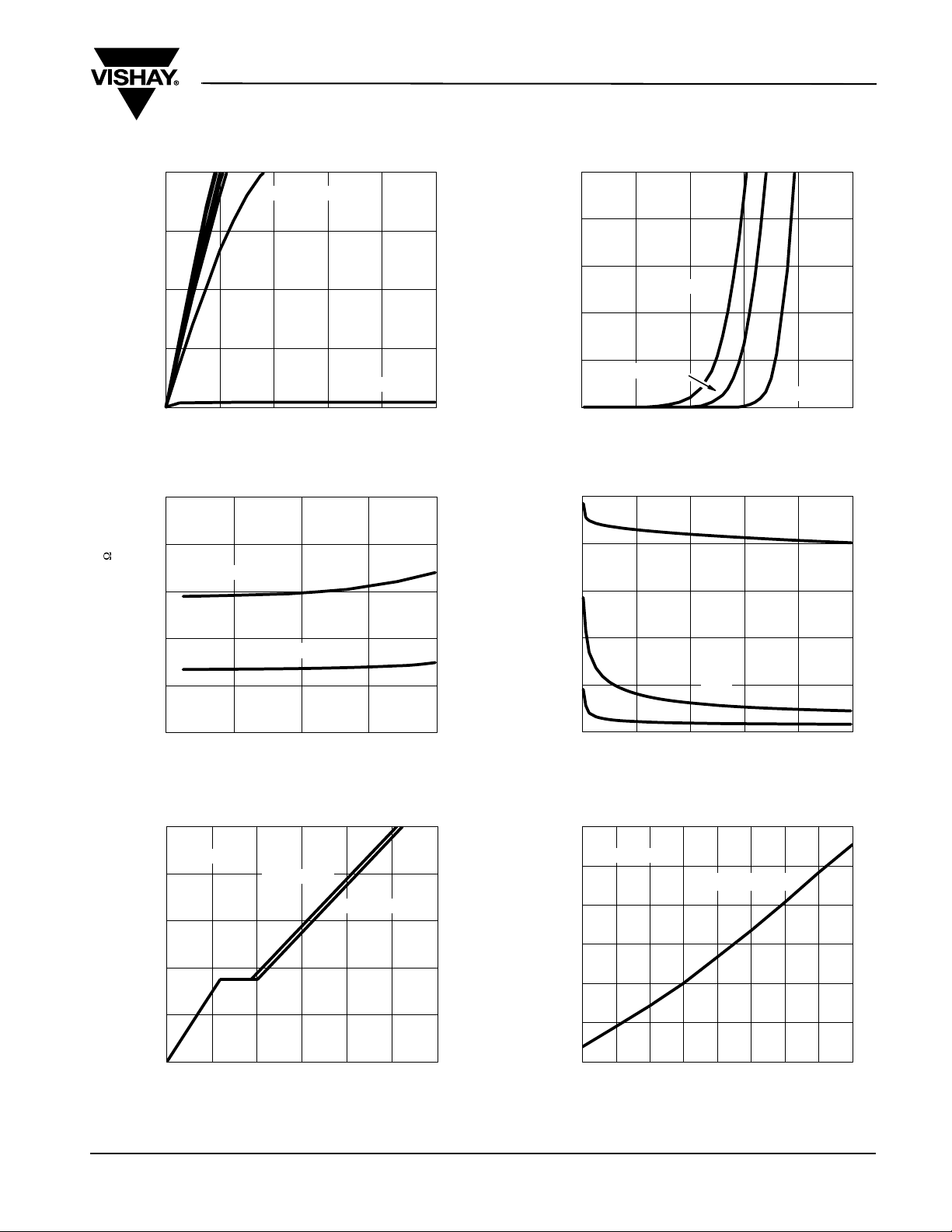
TYPICAL CHARACTERISTICS 25 °C, unless otherwise noted
SiE832DF
Vishay Siliconix
80
VGS = 10 thru 4 V
60
)A( tnerruC niarD -I
40
D
20
0
0.0 0.4 0.8 1.2 1.6 2.0
- Drain-to-Source Voltage (V)
V
DS
Output Characteristics
0.008
0.007
)
( ecnatsiseR-nO
0.006
0.005
-
)no(SD
r
0.004
VGS = 4.5 V
VGS = 10 V
VGS = 3 V
20
16
)A( tnerruC niarD -I
12
TC = 125 °C
8
D
4
0
1.5 2.0 2.5 3.0 3.5 4.0
TC = 25 °C
- Gate-to-Source Voltage (V)
V
GS
Transfer Characteristics
4500
C
oss
3600
)Fp( ecnati
2700
c
a
pa
1800
C -
C
900
C
rss
C
iss
TC = - 55 °C
0.003
0204060
On-Resistance vs. Drain Current
10
)V( e
g
atl
o
V ecruoS-ot-etaG
-
SG
V
ID = 20 A
8
6
4
2
0
0102030405060
Qg - Total Gate Charge (nC)
Gate Charge
Document Number: 74414
S-62483-Rev. A, 04-Dec-06
- Drain Current (A)
I
D
VDS = 20 V
VDS = 32 V
0
80
0 8 16 24 32 40
VDS - Drain-to-Source Voltage (V)
Capacitance
1.8
ID = 14 A
1.6
e
cn
1.4
a
t
)
sis
dez
eR
i
lamr
1.2
nO
-
o
)
N
(
n
o(SD
1.0
r
0.8
0.6
- 50 - 25 0 25 50 75 100 125 150
T
J
VGS = 10 V, 4.5 V
- Junction Temperature (°C)
On-Resistance vs. Junction Temperature
www.vishay.com
3
Page 4

SiE832DF
Vishay Siliconix
TYPICAL CHARACTERISTICS 25 °C, unless otherwise noted
100
)A( tnerruC ecruoS -I
TJ = 150 °C
10
S
1
0.0 0.1 0.2 0.3 0.4 0.5 0.6 0.7 0.8 0.9 1.0 1.1
- Source-to-Drain Voltage (V)
V
SD
Source-Drain Diode Forward Voltage
2.8
2.6
2.4
)
2.2
V(
)ht(
2.0
S
G
V
1.8
ID = 250 µA
TJ = 25 °C
0.012
e (Ω)cnatsiseR-nO ecruoS-ot-niarD -
0.010
0.008
0.006
0.004
)no(SD
r
0.002
246810
V
GS
TA = 25 °C
- Gate-to-Source Voltage (V)
ID = 14 A
TA = 125 °C
On-Resistance vs. Gate-to-Source Voltage
50
40
)W
30
(
rewo
P
20
1.6
1.4
1.2
- 50 - 25 0 25 50 75 100 125 150
- Temperature (°C)
T
J
Threshold Voltage
100
*Limited by r
10
)A
(
t
nerr
u
1
C
n
iar
D
-
D
I
0.1
0.01
0.01
V
*V
GS
Safe Operating Area, Junction-to-Ambient
10
0
Single Pulse Power, Junction-to-Ambient
DS(on)
TA = 25 °C
Single Pulse
BVDSS
Limited
0.1110
- Drain-to-Source Voltage (V)
DS
minimum VGS at which r
DS(on)
isspecified
10 100010.10.01 100
Time (sec)
1 ms
10 ms
100 ms
1 s
10 s
DC
100
www.vishay.com
4
Document Number: 74414
S-62483-Rev. A, 04-Dec-06
Page 5

TYPICAL CHARACTERISTICS 25 °C, unless otherwise noted
SiE832DF
Vishay Siliconix
120
100
)A( tnerruC niarD -
80
60
40
D
I
20
0
Package Limited
0 25 50 75 100 125 150
TC - Case Temperature (°C)
Current Derating*
* The power dissipation PD is based on T
sipation limit for cases where additional heatsinking is used. It is used to determine the current rating, when this rating falls below the package
= 150 °C, using junction-to-case thermal resistance, and is more useful in settling the upper dis-
J(max)
120
100
)W( noitapissiD rewoP
80
60
40
20
0
25 50 75 100 125 150
TC - Case Temperature (°C)
Power Derating, Junction-to-Case
limit.
Document Number: 74414
S-62483-Rev. A, 04-Dec-06
www.vishay.com
5
Page 6

SiE832DF
Vishay Siliconix
TYPICAL CHARACTERISTICS 25 °C, unless otherwise noted
2
tneisnarT evitceffE dezilamroN
1
Duty Cycle = 0.5
ecnadepmI lamrehT
0.2
Notes:
P
DM
t
1
t
– TA = PDMZ
JM
2
1. Duty Cycle, D =
2. Per Unit Base = R
3. T
4. Surface Mounted
thJA
t
t
thJA
100
1
2
= 55 °C/W
(t)
0.1
0.01
0.1
0.05
0.02
Single Pulse
-4
10
-3
10
-2
10
-1
110 60010
Square Wave Pulse Duration (sec)
Normalized Thermal Transient Impedance, Junction-to-Ambient
2
tneisnarT evitceffE de
1
Duty Cycle = 0.5
ecnadepmI lamrehT
0.2
0.1
0.1
z
ilamro
0.05
N
0.02
Single Pulse
0.01
-4
10
-3
10
-2
10
-1
110
Square Wave Pulse Duration (sec)
Normalized Thermal Transient Impedance, Junction-to-Case (Drain Top)
2
tn
e
isn
a
rT
evitcef
f
E d
ezi
lamro
1
Duty Cycle = 0.5
ecnade
0.2
p
mI lamre
h
T
0.1
0.1
0.05
N
0.02
-4
Single Pulse
-3
10
-2
10
-1
110
0.01
10
Square Wave Pulse Duration (sec)
Normalized Thermal Transient Impedance, Junction-to-Source
Vishay Siliconix maintains worldwide manufacturing capability. Products may be manufactured at one of several qualified locations. Reliability data for Silicon Technology and Package Reliability represent a composite of all qualified locations. For related documents such as package/tape drawings, part marking, and reliability
data, see http://www.vishay.com/ppg?74414.
www.vishay.com
6
Document Number: 74414
S-62483-Rev. A, 04-Dec-06
Page 7

Legal Disclaimer Notice
Vishay
Notice
Specifications of the products displayed herein are subject to change without notice. Vishay Intertechnology, Inc.,
or anyone on its behalf, assumes no responsibility or liability for any errors or inaccuracies.
Information contained herein is intended to provide a product description only. No license, express or implied, by
estoppel or otherwise, to any intellectual property rights is granted by this document. Except as provided in Vishay's
terms and conditions of sale for such products, Vishay assumes no liability whatsoever, and disclaims any express
or implied warranty, relating to sale and/or use of Vishay products including liability or warranties relating to fitness
for a particular purpose, merchantability, or infringement of any patent, copyright, or other intellectual property right.
The products shown herein are not designed for use in medical, life-saving, or life-sustaining applications.
Customers using or selling these products for use in such applications do so at their own risk and agree to fully
indemnify Vishay for any damages resulting from such improper use or sale.
Document Number: 91000 www.vishay.com
Revision: 08-Apr-05 1
 Loading...