

Page 1
www.vishay.com
PWM
controller
Gate
driver
5V
V
IN
V
OUT
V
CIN
PWM
V
DRV
V
IN
BOOT
V
SWH
P
GND
GL
C
GND
PHASE
ZCD_EN#
30 A VRPower® Integrated Power Stage
SiC532
Vishay Siliconix
DESCRIPTION
The SiC532 is an integrated power stage solution optimized
for synchronous buck applications to offer high current, high
efficiency, and high power density performance. Packaged
in Vishay’s proprietary 4.5 mm x 3.5 mm MLP package,
SiC532 enables voltage regulator designs to deliver up to
30 A continuous current per phase.
The internal power MOSFETs utilize Vishay’s
state-of-the-art Gen IV TrenchFET
industry benchmark performance to significantly reduce
switching and conduction losses.
The SiC532 incorporates an advanced MOSFET gate driver
IC that features high current driving capability, adaptive
dead-time control, an integrated bootstrap Schottky diode,
and zero current detection to improve light load efficiency.
The driver is also compatible with a wide range of PWM
controllers, supports tri-state PWM, and 5 V PWM logic.
A user selectable diode emulation mode (ZCD_EN#) is
included to improve the light load performance. The device
also supports PS4 mode to reduce power consumption
when system operates in standby state.
®
technology that delivers
FEATURES
• Thermally enhanced PowerPAK® MLP4535-22L
package
• Vishay’s Gen IV MOSFET technology and a
low-side MOSFET with integrated Schottky
diode
• Delivers up to 30 A continuous current, 35 A at 10 ms peak
current
• High efficiency performance
• High frequency operation up to 2 MHz
• Power on reset
• 5 V PWM logic with tri-state and hold-off
• Supports PS4 mode light load requirement for IMVP8 with
low shutdown supply current (5 V, 3 μA)
• Under voltage lockout for V
CIN
• Material categorization: for definitions of compliance
please see www.vishay.com/doc?99912
APPLICATIONS
• Multi-phase VRDs for computing, graphics card and
memory
• Intel IMVP-8 VRPower delivery
- V
- V
• Up to 24 V rail input DC/DC VR modules
CORE
, V
GRAPHICS
, V
platforms
for Apollo Lake platforms
CCGI
SYSTEM AGENT
Skylake, Kabylake
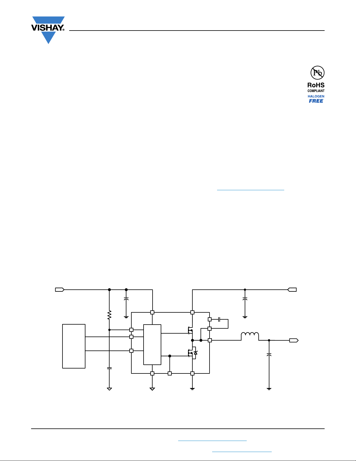
TYPICAL APPLICATION DIAGRAM
S20-0485-Rev. C, 29-Jun-2020
THIS DOCUMENT IS SUBJECT TO CHANGE WITHOUT NOTICE. THE PRODUCTS DESCRIBED HEREIN AND THIS DOCUMENT
ARE SUBJECT TO SPECIFIC DISCLAIMERS, SET FORTH AT www.vishay.com/doc?91000
For technical questions, contact: [email protected]
Fig. 1 - SiC532 Typical Application Diagram
1
Document Number: 74770
Page 2
www.vishay.com
V
V
V
V
V
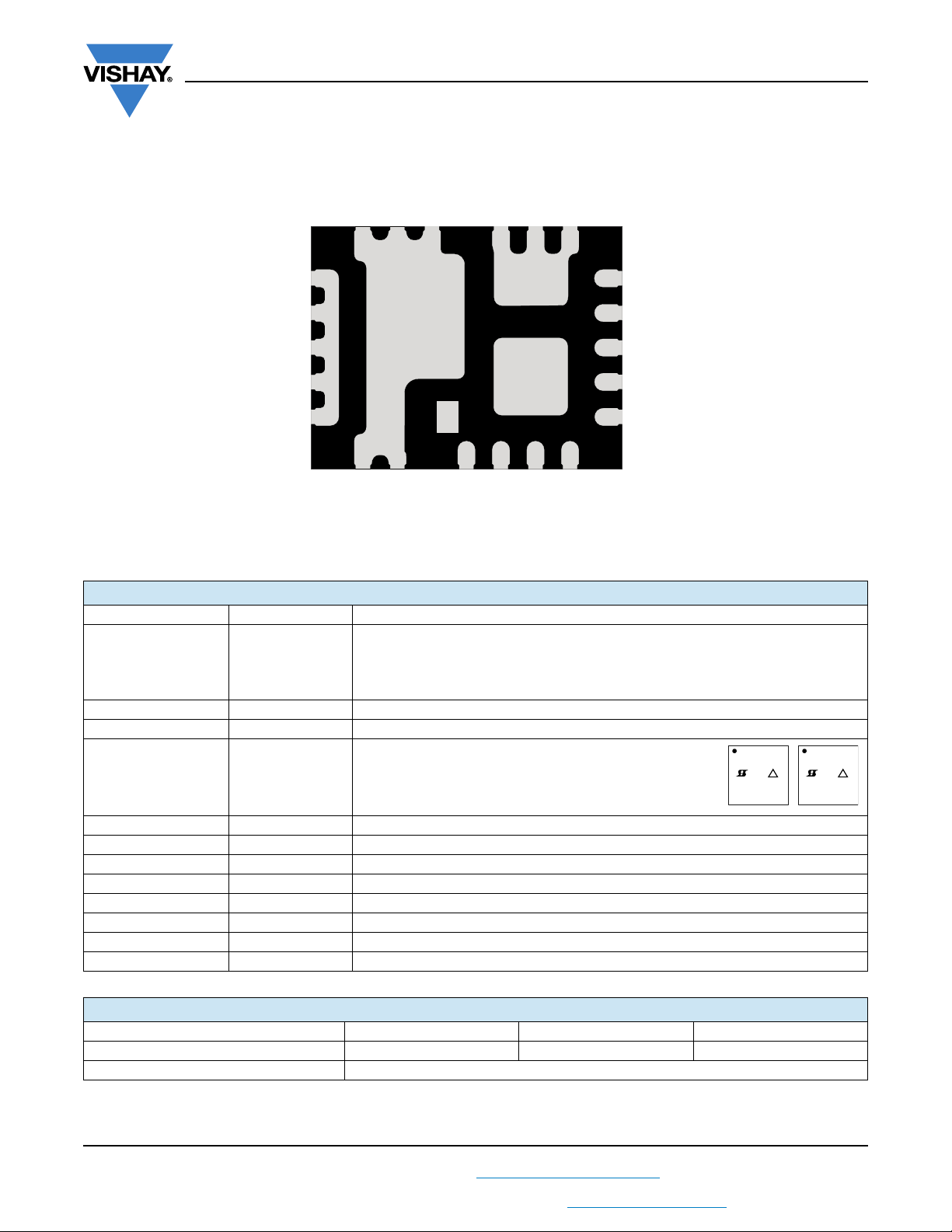
PINOUT CONFIGURATION
SiC532
Vishay Siliconix
SWH
SWH
SWH
SWH
SWH
GNDPGNDPGND
P
11 10 9 8 7 6
12
26
13
14
15
16
P
GND
24
GL
17 18 19 20 21 22
GND
GND
P
P
GL
VINVINV
25
V
23
C
GND
GND
P
IN
PHASE
IN
DRV
V
PWM
5
BOOT
4
3
V
2
ZCD_EN#
1
N.C.
CIN
Fig. 2 - SiC532 Pin Configuration
PIN DESCRIPTION
PIN NUMBER NAME FUNCTION
The ZCD_EN# pin enables or disables Diode Emulation. When ZCD_EN# is LOW, diode
1 ZCD_EN#
2V
23 C
CIN
GND
3N.C.
4 BOOT High-side driver bootstrap voltage
5 PHASE Return path of high-side gate driver
6 to 8, 25 V
9 to 11, 17, 18, 20, 26 P
12 to 16 V
IN
GND
SWH
19, 24 GL Low-side gate signal
21 V
DRV
22 PWM PWM control input
emulation is allowed. When ZCD_EN# is HIGH, continuous conduction mode is forced.
ZCD_EN# can also be put in a high impedance mode by floating the pin. If both ZCD_EN#
and PWM are floating, the device shuts down and consumes typically 3 μA (9 μA max.)
current
Supply voltage for internal logic circuitry
Analog ground for the driver IC
This pin can be either left floating or connected to C
Internally it is either connected to GND or not internally
connected depending on manufacturing location.
Factory code “G” on line 3, pin 3 = C
Factory code “T” on line 3, pin 3 = not internally connected
GND
GND
.
P/N
LL
G Y W W
P/N
LL
T Y W W
Power stage input voltage. Drain of high-side MOSFET
Power ground
Switch node of the power stage
Supply voltage for internal gate driver
ORDERING INFORMATION
PART NUMBER PACKAGE MARKING CODE
SiC532CD-T1-GE3 PowerPAK
®
MLP4535-22L SiC532 5 V PWM optimized
SiC532DB Reference board
S20-0485-Rev. C, 29-Jun-2020
2
Document Number: 74770
For technical questions, contact: [email protected]
THIS DOCUMENT IS SUBJECT TO CHANGE WITHOUT NOTICE. THE PRODUCTS DESCRIBED HEREIN AND THIS DOCUMENT
ARE SUBJECT TO SPECIFIC DISCLAIMERS, SET FORTH AT www.vishay.com/doc?91000
Page 3
SiC532
= pin 1 indicator
P/N = part number code
= Siliconix logo
=ESD symbol
F = assembly factory code
Y = year code
WW = week code
LL = lot code
F Y W W
P/N
LL
www.vishay.com
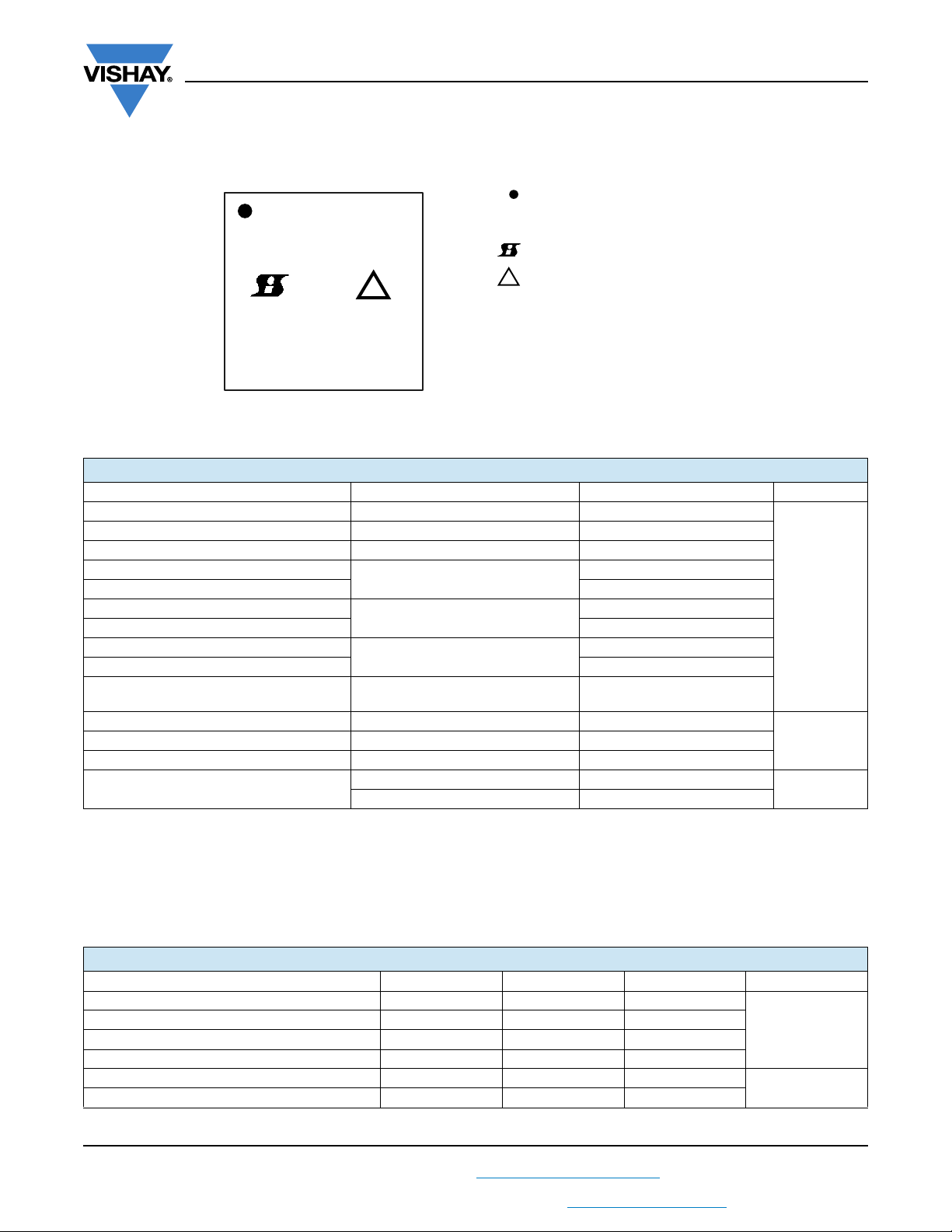
PART MARKING INFORMATION
ABSOLUTE MAXIMUM RATINGS
ELECTRICAL PARAMETER CONDITIONS LIMIT UNIT
Input voltage V
Control logic supply voltage V
Drive supply voltage V
Switch node (DC voltage)
Switch node (AC voltage)
BOOT voltage (DC voltage)
BOOT voltage (AC voltage)
BOOT to PHASE (DC voltage)
BOOT to PHASE (AC voltage)
All logic inputs and outputs
(PWM and ZCD_EN#)
Max. operating junction temperature T
Storage temperature T
Electrostatic discharge protection
Note
• Stresses beyond those listed under “Absolute Maximum Ratings” may cause permanent damage to the device. These are stress ratings
only, and functional operation of the device at these or any other conditions beyond those indicated in the operational sections of the
specifications is not implied. Exposure to absolute maximum rating conditions for extended periods may affect device reliability
(1)
The specification values indicated “AC” is V
(2)
The specification value indicates “AC voltage” is V
(3)
The specification value indicates “AC voltage” is V
(1)
(2)
(3)
Human body model, JESD22-A114 2000
Charged device model, JESD22-C101 1000
to P
SWH
, -8 V (< 20 ns, 10 μJ), min. and 35 V (< 50 ns), max.
GND
to P
BOOT
to V
BOOT
IN
CIN
DRV
V
SWH
V
BOOT
V
BOOT- PHASE
J
A
stg
, 40 V (< 50 ns) max.
GND
, 8 V (< 50 ns) max.
PHASE
-0.3 to +28
-0.3 to +7
-0.3 to +7
-0.3 to +28
-8 to +35
33
40
-0.3 to +7
-0.3 to +8
-0.3 to V
150
-40 to +125
-65 to +150
Vishay Siliconix
+ 0.3
CIN
V
°CAmbient temperature T
V
RECOMMENDED OPERATING RANGE
ELECTRICAL PARAMETER MINIMUM TYPICAL MAXIMUM UNIT
Input voltage (V
Drive supply voltage (V
Control logic supply voltage (V
BOOT to PHASE (V
Thermal resistance from junction to PCB - 5 -
Thermal resistance from junction to case - 2.5 -
S20-0485-Rev. C, 29-Jun-2020
THIS DOCUMENT IS SUBJECT TO CHANGE WITHOUT NOTICE. THE PRODUCTS DESCRIBED HEREIN AND THIS DOCUMENT
)4.5-24
IN
) 4.555.5
DRV
BOOT-PHASE
) 4.555.5
CIN
, DC voltage) 4 4.5 5.5
V
°C/W
For technical questions, contact: [email protected]
ARE SUBJECT TO SPECIFIC DISCLAIMERS, SET FORTH AT www.vishay.com/doc?91000
3
Document Number: 74770
Page 4
www.vishay.com
Vishay Siliconix
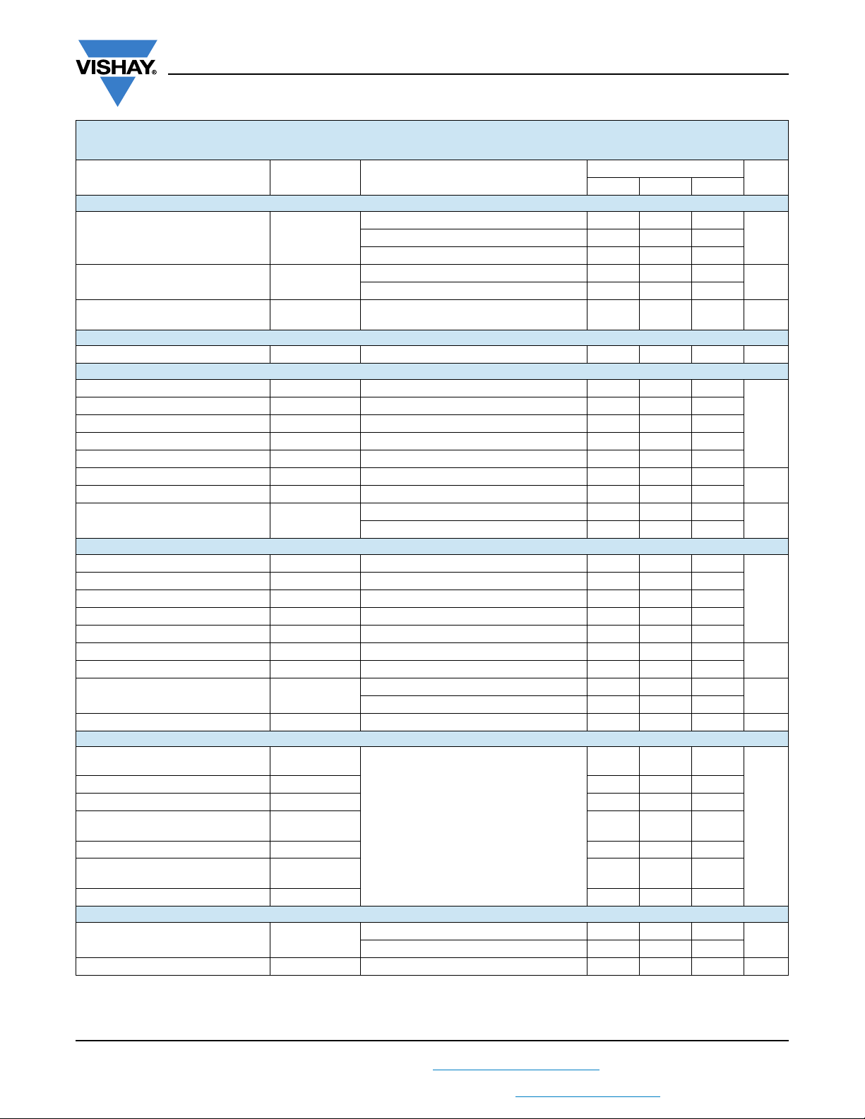
ELECTRICAL SPECIFICATIONS
(ZCD_EN# = 5 V, V
PARAMETER SYMBOL TEST CONDITION
POWER SUPPLY
Control logic supply current I
Drive supply current I
PS4 mode supply current I
BOOTSTRAP SUPPLY
Bootstrap diode forward voltage V
PWM CONTROL INPUT
Rising threshold V
Falling threshold V
Tri-state voltage V
Tri-state rising threshold V
Tri-state falling threshold V
Tri-state rising threshold hysteresis V
Tri-state falling threshold hysteresis V
PWM input current I
ZCD_EN# CONTROL INPUT
Rising threshold V
Falling threshold V
Tri-state voltage V
Tri-state rising threshold V
Tri-state falling threshold V
Tri-state rising threshold hysteresis V
Tri-state falling threshold hysteresis V
ZCD_EN# input current I
PS4 exit latency t
TIMING SPECIFICATIONS
Tri-state to GH/GL rising
propagation delay
Tri-state hold-off time t
GH - turn off propagation delay t
GH - turn on propagation delay
(dead time rising)
GL - turn off propagation delay t
GL - turn on propagation delay
(dead time falling)
PWM minimum on-time T
PROTECTION
Under voltage lockout V
Under voltage lockout hysteresis V
Notes
(1)
Typical limits are established by characterization and are not production tested
(2)
Guaranteed by design
S20-0485-Rev. C, 29-Jun-2020
THIS DOCUMENT IS SUBJECT TO CHANGE WITHOUT NOTICE. THE PRODUCTS DESCRIBED HEREIN AND THIS DOCUMENT
= 12 V, V
IN
DRV
and V
= 5 V, TA = 25 °C, unless otherwise stated)
CIN
LIMITS
MIN. TYP. MAX.
V
= FLOAT - 80 -
PWM
VCIN
VDRV
+ I
VCIN
VDRV
F
TH_PWM_R
TH_PWM_F
TRI
TRI_TH_R
TRI_TH_F
HYS_TRI_R
HYS_TRI_F
PWM
TH_ZCD_EN#_R
TH_ZCD_EN#_F
TRI_ZCD_EN#
TRI_ZCD_EN#_R
TRI_ZCD_EN#_F
HYS_TRI_ZCD#_R
HYS_TRI_ZCD#_F
ZCD_EN#
PS4EXIT
t
PD_TRI_R
TSHO
PD_OFF_GH
t
PD_ON_GH
PD_OFF_GL
t
PD_ON_GL
PWM_ON_MIN
UVLO
UVLO_HYST
= FLOAT, V
PWM
f
= 300 kHz, D = 0.1 - 300 -
S
fS = 300 kHz, D = 0.1 - 10 15
= 1 MHz, D = 0.1 - 20 -
f
S
V
= V
PWM
ZCD_EN#
T
= -10 °C to +100 °C
A
IF = 2 mA - - 0.65 V
V
= FLOAT - 2.5 -
PWM
V
= 5 V - - 350
PWM
= 0 V - - -350
V
PWM
V
= FLOAT - 2.5 -
ZCD_EN#
V
ZCD_EN#
V
ZCD_EN#
No load, see fig. 4
V
rising, on threshold - 3.4 3.9
CIN
falling, off threshold 2.4 2.9 -
V
CIN
= 0 V - 120 -
ZCD_EN#
= FLOAT,
-39μA
3.6 3.9 4.2
0.72 1 1.3
1.11.351.6
3.4 3.7 4
- 325 -
- 250 -
3.3 3.6 3.9
1.1 1.4 1.7
1.5 1.8 2.1
2.93.153.4
- 375 -
- 450 -
= 5 V - - 100
= 0 V - - -100
--5μs
-20-
- 150 -
-20-
-20-
-20-
-20-
30 - -
- 500 - mV
4
For technical questions, contact: [email protected]
ARE SUBJECT TO SPECIFIC DISCLAIMERS, SET FORTH AT www.vishay.com/doc?91000
Document Number: 74770
SiC532
UNIT
μAV
mA
V
mV
μA
V
mV
μA
ns
V
Page 5

www.vishay.com
DETAILED OPERATIONAL DESCRIPTION
PWM Input with Tri-state Function
The PWM input receives the PWM control signal from the VR
controller IC. The PWM input is designed to be compatible
with standard controllers using two state logic (H and L) and
advanced controllers that incorporate tri-state logic (H, L,
and tri-state) on the PWM output. For two state logic, the
PWM input operates as follows. When PWM is driven above
V
PWM_TH_R
turned on. When PWM input is driven below V
high-side is turned off and the low-side is turned on. For
tri-state logic, the PWM input operates as previously stated
for driving the MOSFETs when PWM is logic high and logic
low. However, there is a third state that is entered as the
PWM output of tri-state compatible controller enters its high
impedance state during shut-down. The high impedance
state of the controller’s PWM output allows the SiC532 to
pull the PWM input into the tri-state region (see definition of
PWM logic and tri-state, fig. 4). If the PWM input stays in this
region for the tri-state hold-off period, t
and low-side MOSFETs are turned off. The function allows
the VR phase to be disabled without negative output voltage
swing caused by inductor ringing and saves a Schottky
diode clamp. The PWM and tri-state regions are separated
by hysteresis to prevent false triggering. The SiC532
incorporates PWM voltage thresholds that are compatible
with 5 V logic.
Diode Emulation Mode and PS4 Mode (ZCD_EN#)
The ZCD_EN# pin enables or disables diode emulation
mode. When ZCD_EN# is driven below V
emulation is allowed. When ZCD_EN# is driven above
V
TH_ZCD_EN#_R
Diode emulation mode allows for higher converter efficiency
under light load situations. With diode emulation active, the
SiC532 will detect the zero current crossing of the output
inductor and turn off the low-side MOSFET. This ensures
that discontinuous conduction mode (DCM) is achieved.
Diode emulation is asynchronous to the PWM signal,
therefore, the SiC532 will respond to the ZCD_EN# input
immediately after it changes state.
The ZCD_EN# pin can be floated resulting in a high
impedance state. High impedance on the input of ZCD_EN#
combined with a tri-stated PWM output will shut down the
SiC532, reducing current consumption to typically 5 μA.
This is an important feature in achieving the low standby
current requirements required in the PS4 state in ultrabooks
and notebooks.
Voltage Input (V
This is the power input to the drain of the high-side power
MOSFET. This pin is connected to the high power
intermediate BUS rail.
the low-side is turned off and the high-side is
PWM_TH_F
, both high-side
TSHO
TH_ZCD_EN#_F
the
, diode
, continuous conduction mode is forced.
)
IN
SiC532
Vishay Siliconix
Switch Node (V
The switch node, V
This is the output applied to the power inductor and output
filter to deliver the output for the buck converter. The PHASE
pin is internally connected to the switch node, V
is to be used exclusively as the return pin for the BOOT
capacitor.
Ground Connections (C
P
(power ground) should be externally connected to
GND
C
(control signal ground). The layout of the printed circuit
GND
board should be such that the inductance separating C
and P
is minimized. Transient differences due to
GND
inductance effects between these two pins should not
exceed 0.5 V.
Control and Drive Supply Voltage Input (V
V
is the bias supply for the gate drive control IC. V
CIN
the bias supply for the gate drivers. It is recommended to
separate these pins through a resistor. This creates a low
pass filtering effect to avoid coupling of high frequency gate
drive noise into the IC.
Bootstrap Circuit (BOOT)
The internal bootstrap diode and an external bootstrap
capacitor form a charge pump that supplies voltage to the
BOOT pin. An integrated bootstrap diode is incorporated so
that only an external capacitor is necessary to complete the
bootstrap circuit. Connect a boot strap capacitor with one
leg tied to BOOT pin and the other tied to PHASE pin.
Shoot-through Protection and Adaptive Dead Time
The SiC532 has an internal adaptive logic to avoid shoot
through and optimize dead time. The shoot through
protection ensures that both high-side and low-side
MOSFETs are not turned on at the same time. The adaptive
dead time control operates as follows. The high-side and
low-side gate voltages are monitored to prevent the
MOSFET turning on from tuning on until the other
MOSFET’s gate voltage is sufficiently low (< 1 V). Built in
delays also ensure that one power MOSFET is completely
off, before the other can be turned on. This feature helps to
adjust dead time as gate transitions change with respect to
output current and temperature.
Under Voltage Lockout (UVLO)
During the start up cycle, the UVLO disables the gate
drive, holding high-side and low-side MOSFET gates low,
until the supply voltage rail has reached a point at which
the logic circuitry can be safely activated. The SiC532 also
incorporates logic to clamp the gate drive signals to zero
when the UVLO falling edge triggers the shutdown of the
device.
and PHASE)
SWH
, is the circuit power stage output.
SWH
GND
and P
GND
. This pin
SWH
)
GND
, V
CIN
)
DRV
is
DRV
S20-0485-Rev. C, 29-Jun-2020
For technical questions, contact: [email protected]
THIS DOCUMENT IS SUBJECT TO CHANGE WITHOUT NOTICE. THE PRODUCTS DESCRIBED HEREIN AND THIS DOCUMENT
ARE SUBJECT TO SPECIFIC DISCLAIMERS, SET FORTH AT www.vishay.com/doc?91000
5
Document Number: 74770
Page 6
www.vishay.com
ZCD_EN#
V
SWH
GL
+
-
GL
+
-
UVLO
V
CIN
PWM logic
control &
state
machine
Anti-cross
conduction
control
logic
BOOT
V
IN
PWM
C
GND
V
CIN
P
GND
PHASE
V
DRV
V
DRV
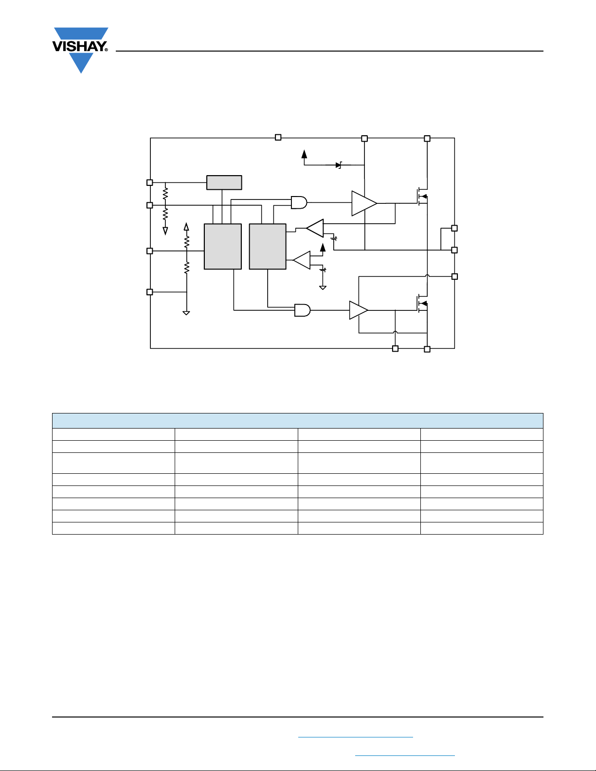
FUNCTIONAL BLOCK DIAGRAM
SiC532
Vishay Siliconix
Fig. 3 - SiC532 Functional Block Diagram
DEVICE TRUTH TABLE
ZCD_EN# PWM GH GL
Hi-Z (PS4 mode) X L L
LLL
LHHL
LHi-ZL L
HLLH
HHHL
HHi-ZL L
S20-0485-Rev. C, 29-Jun-2020
6
For technical questions, contact: [email protected]
THIS DOCUMENT IS SUBJECT TO CHANGE WITHOUT NOTICE. THE PRODUCTS DESCRIBED HEREIN AND THIS DOCUMENT
ARE SUBJECT TO SPECIFIC DISCLAIMERS, SET FORTH AT www.vishay.com/doc?91000
H, I
L, I
Document Number: 74770
> 0 A
L
< 0 A
L
Page 7
www.vishay.com
V
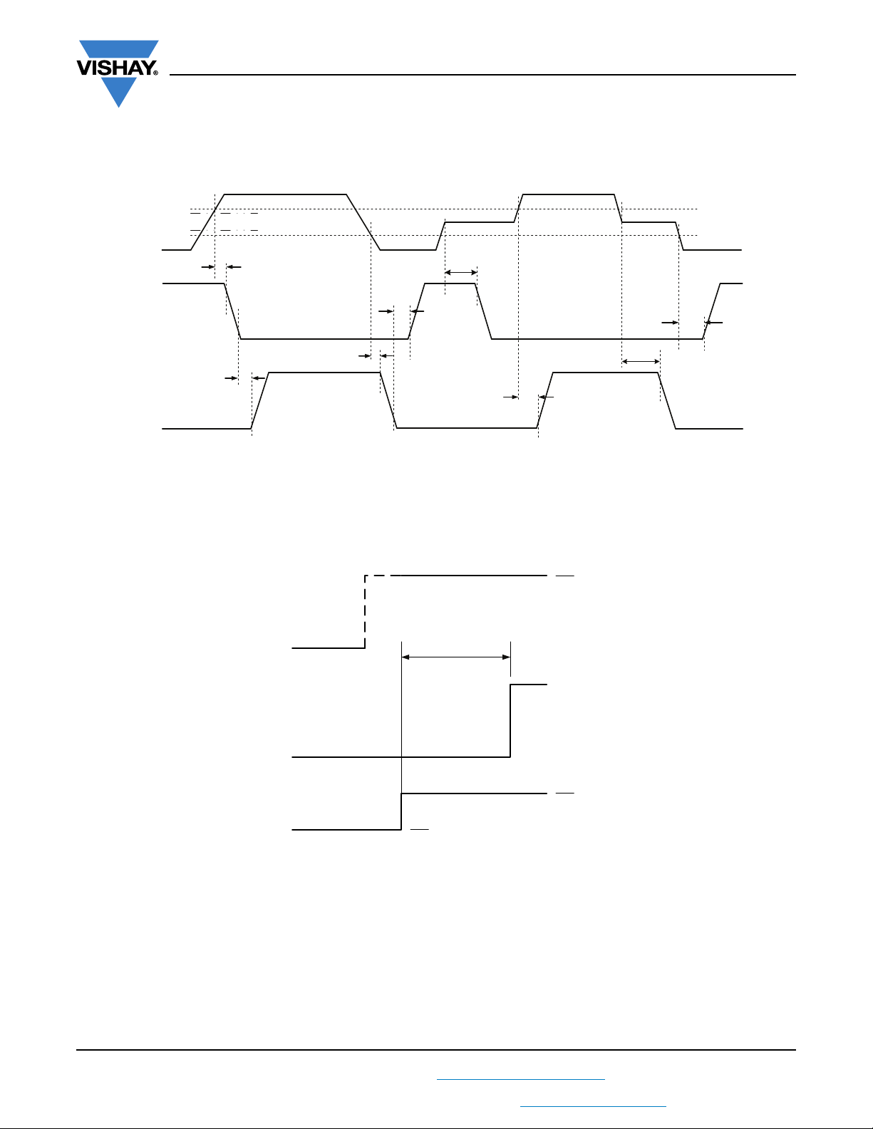
PWM TIMING DIAGRAM
V
TH_PWM_R
V
TH_PWM_F
PWM
GL
GH
t
PD_OFF_GL
V
TH_TRI_F
V
TH_TRI_R
t
PD_ON_GH
t
PD_OFF_GH
t
PD_ON_GL
t
TSHO
t
PD_TRI_R
SiC532
Vishay Siliconix
t
PD_TRI_R
t
TSHO
ZCD_EN# - PS4 EXIT TIMING
PWM
ZCD_EN#
Fig. 4 - Definition of PWM Logic and Tri-State
t
PS4EXIT
V
SWH
2.5 V
Fig. 5 - ZCD_EN# - PS4 Exit Timing
5
V
5
S20-0485-Rev. C, 29-Jun-2020
For technical questions, contact: [email protected]
THIS DOCUMENT IS SUBJECT TO CHANGE WITHOUT NOTICE. THE PRODUCTS DESCRIBED HEREIN AND THIS DOCUMENT
ARE SUBJECT TO SPECIFIC DISCLAIMERS, SET FORTH AT www.vishay.com/doc?91000
7
Document Number: 74770
Page 8
www.vishay.com
62
66
70
74
78
82
86
90
94
0 5 10 15 20 25 30
Efciency (%)
Output Current, I
OUT
(A)
Complete converter efciency
P
IN
= [(VINx IIN) + 5 V x (I
VDRV
+ I
VCIN
)]
P
OUT
= V
OUT
x I
OUT
, measured at output capacitor
1MHz
750 kHz
500 kHz
2.0
2.5
3.0
3.5
4.0
4.5
5.0
5.5
6.0
200 300 400 500 600 700 800 900 1000 1100
Power Loss, P
L
(W)
Switching Frequency, fS (kHz)
I
OUT
= 25 A
62
66
70
74
78
82
86
90
94
0 5 10 15 20 25 30
Efciency (%)
Output Current, I
OUT
(A)
Complete converter efciency
P
IN
= [(VINx IIN) + 5 V x (I
VDRV
+ I
VCIN
)]
P
OUT
= V
OUT
x I
OUT
, measured at output capacitor
1 MHz
750 kHz
500 kHz
0
5
10
15
20
25
30
35
40
0 153045607590105120135150
Output Current, I
OUT
(A)
PCB Temperature, T
PCB
(°C)
1 MHz
500 kHz
62
66
70
74
78
82
86
90
94
0 5 10 15 20 25 30
Efciency (%)
Output Current, I
OUT
(A)
Complete converter efciency
P
IN
= [(VINx IIN) + 5 V x (I
VDRV
+ I
VCIN
)]
P
OUT
= V
OUT
x I
OUT
, measured at output capacitor
1 MHz
500 kHz
750 kHz
ELECTRICAL CHARACTERISTICS
Test condition: VIN = 13 V, V
(All power loss and normalized power loss curves show SiC532 losses only unless otherwise stated)
DRV
= V
= 5 V, ZCD_EN# = 5 V, V
CIN
OUT
= 1 V, L
= 250 nH, (DCR = 0.32 m), TA = 25 °C
OUT
SiC532
Vishay Siliconix
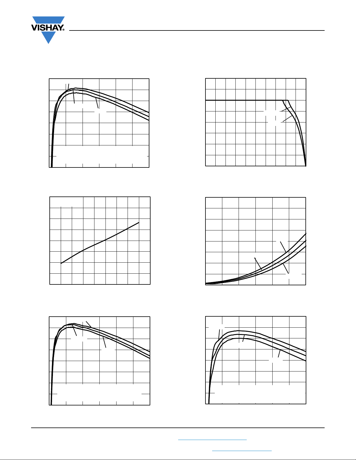
Fig. 6 - Efficiency vs. Output Current (V
= 12.6 V)
IN
Fig. 7 - Power Loss vs. Switching Frequency (V
= 12.6 V)
IN
Fig. 9 - Safe Operating Area (V
IN
12.0
10.5
9.0
(W)
L
7.5
1 MHz
Power Loss, P
6.0
4.5
750 kHz
3.0
1.5
0.0
0 5 10 15 20 25 30
Output Current, I
OUT
(A)
Fig. 10 - Power Loss vs. Output Current (V
= 12.6 V)
500 kHz
= 12.6 V)
IN
Fig. 8 - Efficiency vs. Output Current (V
S20-0485-Rev. C, 29-Jun-2020
THIS DOCUMENT IS SUBJECT TO CHANGE WITHOUT NOTICE. THE PRODUCTS DESCRIBED HEREIN AND THIS DOCUMENT
ARE SUBJECT TO SPECIFIC DISCLAIMERS, SET FORTH AT www.vishay.com/doc?91000
= 9 V)
IN
Fig. 11 - Efficiency vs. Output Current (V
8
For technical questions, contact: [email protected]
= 19 V)
IN
Document Number: 74770
Page 9
www.vishay.com
2.6
2.8
3.0
3.2
3.4
3.6
3.8
4.0
4.2
-60 -40 -20 0 20 40 60 80 100 120 140
Control Logic Supply Voltage, V
CIN
(V)
Temperature (°C)
V
UVLO_FALLING
V
UVLO_RISING
3
4
5
6
7
8
9
10
11
-60 -40 -20 0 20 40 60 80 100 120 140
Driver
S
upply Current, I
VDRV
(mA)
Temperature (°C)
f
PWM
= 300 kHz
0.0
0.6
1.2
1.8
2.4
3.0
3.6
4.2
4.8
-60 -40 -20 0 20 40 60 80 100 120 140
ZCD_EN# Threshold Voltage, V
ZCD_EN#
(V)
Temperature (°C)
V
TRI_ZCD_EN#_R
V
TRI_ZCD_EN#_ F
V
TH_ZCD_EN#_R
V
TH_ZCD_EN#_F
ELECTRICAL CHARACTERISTICS
Test condition: VIN = 13 V, V
(All power loss and normalized power loss curves show SiC532 losses only unless otherwise stated)
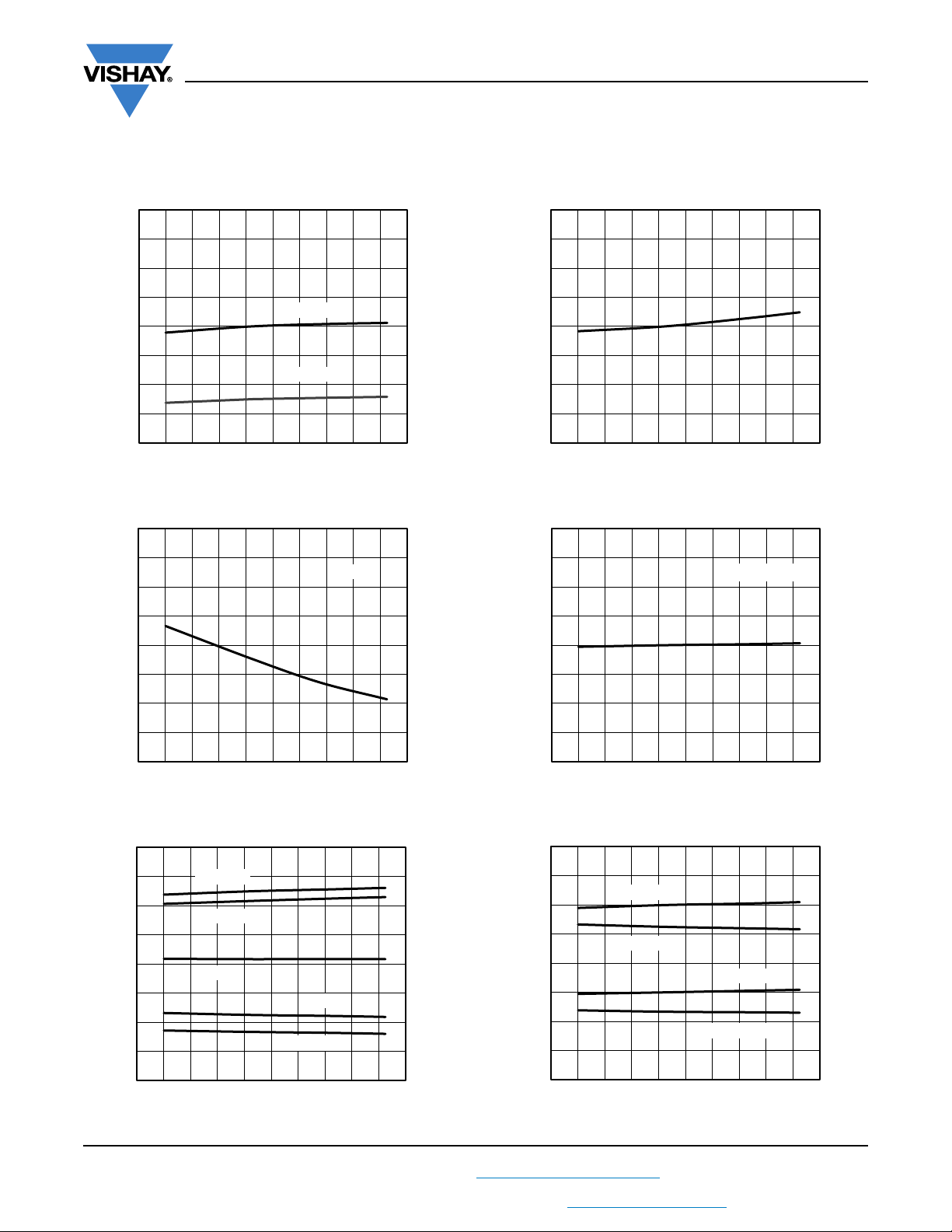
Fig. 12 - UVLO Threshold vs. Temperature
DRV
= V
= 5 V, ZCD_EN# = 5 V, V
CIN
OUT
= 1 V, L
= 250 nH, (DCR = 0.32 m), TA = 25 °C
OUT
1.8
1.6
PS4EXIT
1.4
1.2
1.0
0.8
0.6
Normalized PS4 Exit Latency, t
0.4
0.2
-60 -40 -20 0 20 40 60 80 100 120 140
Fig. 15 - PS4 Exit Latency vs. Temperature
SiC532
Vishay Siliconix
Temperature (°C)
0.80
0.75
(V)
F
0.70
0.65
0.60
0.55
0.50
0.45
BOOT Diode Forward Voltage, V
0.40
-60 -40 -20 0 20 40 60 80 100 120 140
Temperature (°C)
Fig. 13 - BOOT Diode Forward Voltage vs. Temperature
4.8
4.2
(V)
3.6
PWM
3.0
2.4
1.8
1.2
PWM Threshold Voltage, V
0.6
0.0
-60 -40 -20 0 20 40 60 80 100 120 140
Fig. 14 - PWM Threshold vs. Temperature
S20-0485-Rev. C, 29-Jun-2020
THIS DOCUMENT IS SUBJECT TO CHANGE WITHOUT NOTICE. THE PRODUCTS DESCRIBED HEREIN AND THIS DOCUMENT
V
TH_PWM_R
V
TRI_TH_F
V
TRI
Temperature (°C)
ARE SUBJECT TO SPECIFIC DISCLAIMERS, SET FORTH AT www.vishay.com/doc?91000
IF= 2 mA
Fig. 16 - Driver Supply Current vs. Temperature
V
TRI_TH_R
V
TH_PWM_F
Fig. 17 - ZCD_EN# Threshold vs. Temperature
9
For technical questions, contact: [email protected]
Document Number: 74770
Page 10
www.vishay.com
P
GND
Plane
V
SWH
Snubber
P
GND
C
vcin
C
vdrv
A
GND
Cboot
Rboot
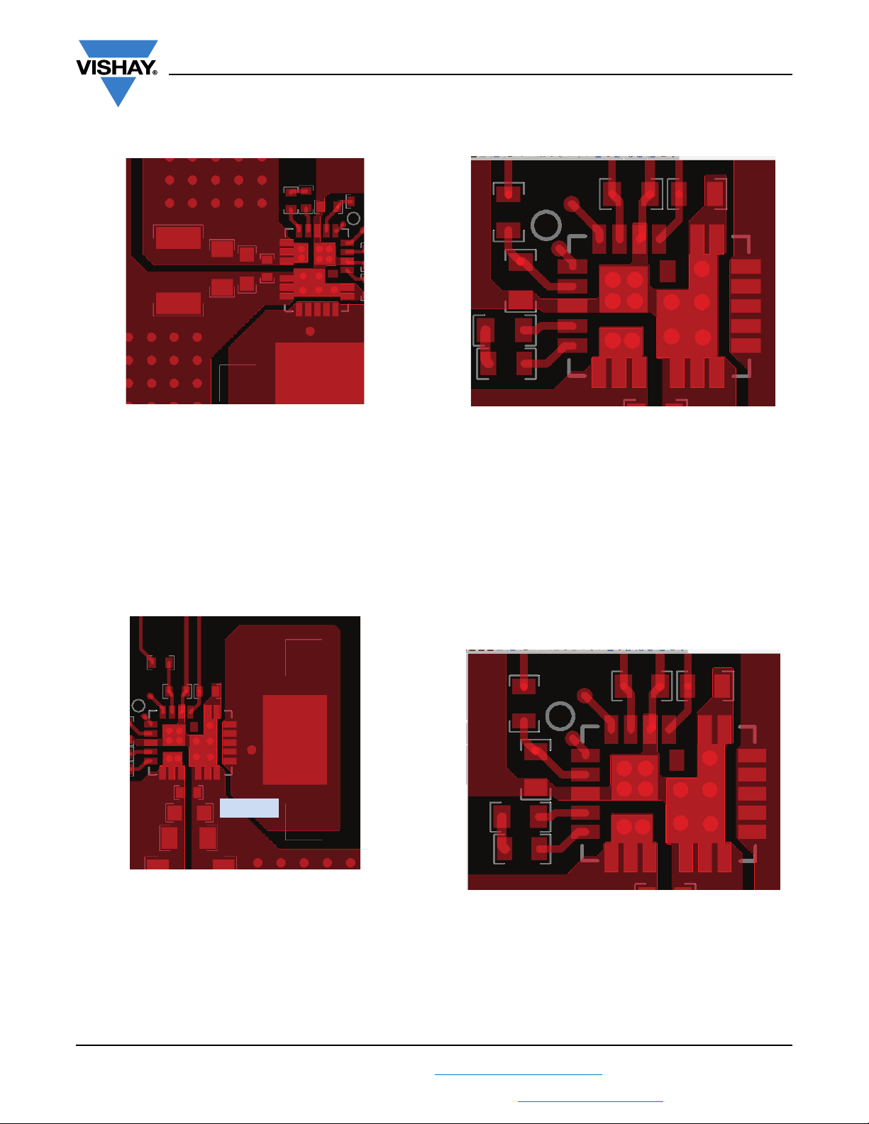
PCB LAYOUT RECOMMENDATIONS
Step 1: VIN / P
Planes and Decoupling
GND
VINPlane
P
V
IN
V
SWH
Plane
P
GND
SiC532
Vishay Siliconix
/ V
Step 3: V
GND
CIN
Input Filter
DRV
1. Layout VIN and P
planes as shown above.
GND
2. Ceramic capacitors should be placed directly between
VIN and P
, and close to the device for best
GND
decoupling effect.
3. Different values / packages of ceramic capacitors should
be used to cover entire decoupling spectrum e.g. 1210,
0805, 0603, 0402.
4. Smaller capacitance values, placed closer to the
device’s VIN pin(s), results in better high frequency noise
absorbing.
Step 2: V
SWH
Plane
1. The V
CIN
/ V
input filter ceramic cap should be placed
DRV
as close as possible to the IC. It is recommended to
connect two capacitors separately.
2. V
capacitor should be placed between pin 2 (V
CIN
and pin 3 (A
of driver IC) to achieve best noise
GND
filtering.
3. V
capacitor should be placed between pin 20
DRV
(P
of driver IC) and pin 21 (V
GND
) to provide maximum
DRV
instantaneous driver current for low side MOSFET during
switching cycle.
4. For connecting V
CIN
to A
, it is recommended to use
GND
a large plane to reduce parasitic inductance.
Step 4: BOOT Resistor and Capacitor Placement
CIN
)
1. Connect output inductor to IC with large plane to lower
resistance.
2. V
plane also serves as a heat-sink for low-side
SWH
MOSFET. Make the plane wide and short to achieve the
best thermal path.
1. The components need to be placed as close as possible
to IC, directly between PHASE (pin 5) and BOOT (pin 4).
2. To reduce parasitic inductance, chip size 0402 can be
used.
3. If a snubber network is required, place the components
as shown above, the network can be placed at bottom.
S20-0485-Rev. C, 29-Jun-2020
THIS DOCUMENT IS SUBJECT TO CHANGE WITHOUT NOTICE. THE PRODUCTS DESCRIBED HEREIN AND THIS DOCUMENT
ARE SUBJECT TO SPECIFIC DISCLAIMERS, SET FORTH AT www.vishay.com/doc?91000
For technical questions, contact: [email protected]
10
Document Number: 74770
Page 11
www.vishay.com
P
GND
A
GND
A
GND
SiC532
Vishay Siliconix
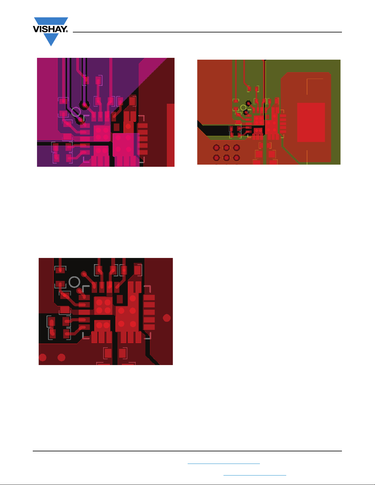
Step 5: Signal Routing
1. Route the PWM and ZCD_EN# signal traces out of the
top left corner next to pin 1.
2. The PWM signal is an important signal, both signal and
return traces should not cross any power nodes on any
layer.
3. It is best to “shield” these traces from power switching
nodes, e.g. V
, with a GND island to improve signal
SWH
integrity.
4. GL (pin 19) has been connected with GL pad (pin 24)
internally.
Step 7: Ground Connection
A
GND
P
GND
V
SWH
1. It is recommended to make a single connection between
A
GND
and P
which can be made on the top layer.
GND
2. It is recommended to make the entire first inner layer
(below top layer) the ground plane and separate them
into A
GND
and P
GND
planes.
3. These ground planes provide shielding between noise
sources on top layer and signal traces on bottom layer.
Step 6: Adding Thermal Relief Vias
A
GND
P
GND
V
IN
Plane
P
GND
VINPlane
1. Thermal relief vias can be added on the VIN and A
pads to utilize inner layers for high-current and thermal
dissipation.
2. To achieve better thermal performance, additional vias
can be placed on VIN plane and P
3. V
pad is a noise source, it is not recommended to
SWH
GND
plane.
place vias on this pad.
4. 8 mil vias for pads and 10 mils vias for planes are the
optimal via sizes. Vias on pad may drain solder during
assembly and cause assembly issues. Consult with the
assembly house for guidelines.
S20-0485-Rev. C, 29-Jun-2020
THIS DOCUMENT IS SUBJECT TO CHANGE WITHOUT NOTICE. THE PRODUCTS DESCRIBED HEREIN AND THIS DOCUMENT
For technical questions, contact: [email protected]
ARE SUBJECT TO SPECIFIC DISCLAIMERS, SET FORTH AT www.vishay.com/doc?91000
V
SWH
GND
11
Document Number: 74770
Page 12
www.vishay.com
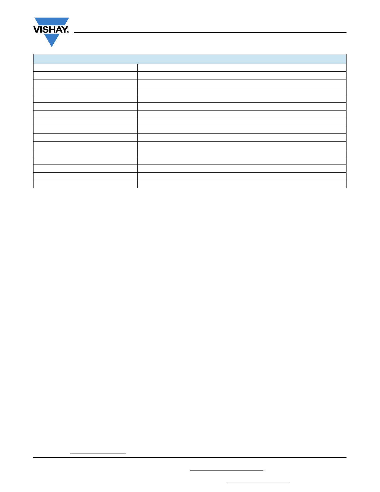
PRODUCT SUMMARY
Part number SiC532
Description 30 A power stage, 4.5 V
Input voltage min. (V) 4.5
Input voltage max. (V) 24
Continuous current rating max. (A) 30
Switch frequency max. (kHz) 2000
Enable (yes / no) No
Monitoring features -
Protection UVLO, THDN
Light load mode ZCD, PS4
Pulse-width modulation (V) 5
Package type PowerPAK MLP4535-22L
Package size (W, L, H) (mm) 4.5 x 3.5 x 0.75
Status code 2
Product type VRPower (DrMOS)
Applications Computer, industrial, networking
to 24 VIN, 5 V PWM with ZCD, PS4 mode
IN
SiC532
Vishay Siliconix
Vishay Siliconix maintains worldwide manufacturing capability. Products may be manufactured at one of several qualified locations. Reliability data for Silicon
Technology and Package Reliability represent a composite of all qualified locations. For related documents such as package / tape drawings, part marking, and
reliability data, see www.vishay.com/ppg?74770
S20-0485-Rev. C, 29-Jun-2020
For technical questions, contact: [email protected]
THIS DOCUMENT IS SUBJECT TO CHANGE WITHOUT NOTICE. THE PRODUCTS DESCRIBED HEREIN AND THIS DOCUMENT
ARE SUBJECT TO SPECIFIC DISCLAIMERS, SET FORTH AT www.vishay.com/doc?91000
12
Document Number: 74770
Page 13
www.vishay.com
9
14
1
1110
5
4
3
2
16
1719
8227
15
2021
6
13
18
12
9
14
1
11 10
5
4
3
2
16
17 19
8227
15
20 21
6
13
18
12
D
E
A
A1
A2
b
e
L
D2-1
D2-2D2-3
D2-4
E2-1
E2-2E2-3
E2-4
K1
K2
A
Pin 1 dot
by marking
C
56
B
K3
D1-1
E1-1
E1-2
D1-2
K4
E1-4
E1-3
E1-5
0.1
C
B
2x
0.1
C
A
2x
0.08
C
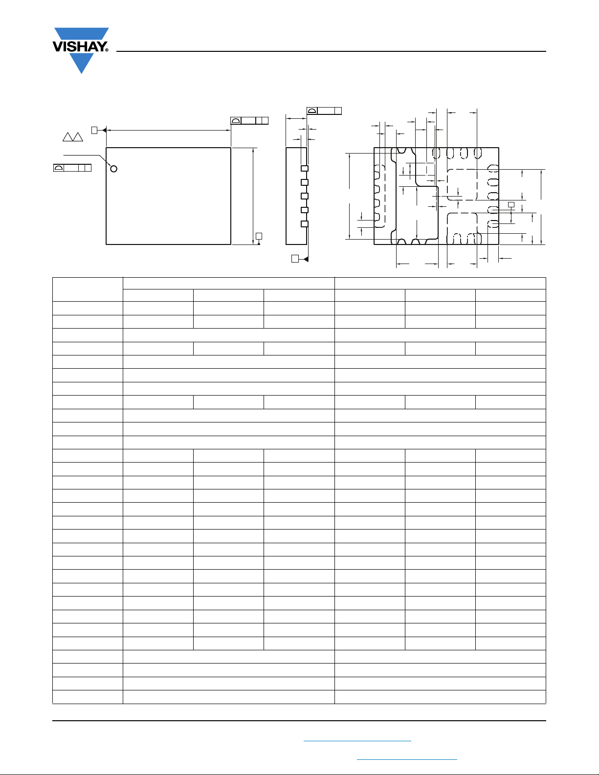
MLP 4.5 x 3.5-22L BWL Case Outline
Package Information
Vishay Siliconix
Revision: 20-Oct-14
DIM.
(8)
A
MIN. NOM. MAX. MIN. NOM. MAX.
0.70 0.75 0.80 0.027 0.0029 0.031
MILLIMETERS INCHES
A1 0.00 - 0.05 0.000 - 0.002
A2 0.20 ref. 0.008 ref.
(4)
b
0.20 0.25 0.30 0.0078 0.0098 0.0110
D 4.50 BSC 0.177 BSC
e 0.50 BSC 0.019 BSC
E 3.50 BSC 0.137 BSC
L 0.35 0.40 0.45 0.013 0.015 0.017
Nd
Ne
(3)
N
(3)
(3)
22 22
66
55
D1-1 0.35 0.40 0.45 0.013 0.015 0.017
D1-2 0.15 0.20 0.25 0.005 0.007 0.009
D2-1 1.02 1.07 1.12 0.040 0.042 0.044
D2-2 1.02 1.07 1.12 0.040 0.042 0.044
D2-3 1.47 1.52 1.57 0.057 0.059 0.061
D2-4 0.25 0.30 0.35 0.009 0.011 0.013
E1-1 1.095 1.145 1.195 0.043 0.045 0.047
E1-2 2.67 2.72 2.77 0.105 0.107 0.109
E1-3 0.35 0.40 0.45 0.013 0.015 0.017
E1-4 1.85 1.90 1.95 0.072 0.074 0.076
E1-5 0.095 0.145 0.195 0.0037 0.0057 0.0076
E2-1 3.05 3.10 3.15 0.120 0.122 0.124
E2-2 1.065 1.115 1.165 0.0419 0.0438 0.0458
E2-3 0.695 0.745 0.795 0.027 0.029 0.031
E2-4 0.40 0.45 0.50 0.015 0.017 0.019
K1 0.40 BSC 0.015 BSC
K2 0.07 BSC 0.002 BSC
K3 0.05 BSC 0.001 BSC
K4 0.40 BSC 0.015 BSC
THIS DOCUMENT IS SUBJECT TO CHANGE WITHOUT NOTICE. THE PRODUCTS DESCRIBED HEREIN AND THIS DOCUMENT
ARE SUBJECT TO SPECIFIC DISCLAIMERS, SET FORTH AT www.vishay.com/doc?91000
For technical questions, contact: [email protected]
1
Document Number: 67234
Page 14

Package Information
www.vishay.com
Notes
1. Use millimeters as the primary measurement
2. Dimensioning and tolerances conform to ASME Y14.5M. - 1994
3. N is the number of terminals,
Nd is the number of terminals in X-direction and
Ne is the number of terminals in Y-direction.
4. Dimension b applies to plated terminal and is measured between 0.20 mm and 0.25 mm from terminal tip
5. The pin #1 identifier must be existed on the top surface of the package by using indentation mark or other feature of package body
6. Exact shape and size of this feature is optional
7. Package warpage max. 0.08 mm
8. Applied only for terminals
T14-0626-Rev. A, 20-Oct-14
DWG: 6028
Vishay Siliconix
Revision: 20-Oct-14
For technical questions, contact: [email protected]
THIS DOCUMENT IS SUBJECT TO CHANGE WITHOUT NOTICE. THE PRODUCTS DESCRIBED HEREIN AND THIS DOCUMENT
ARE SUBJECT TO SPECIFIC DISCLAIMERS, SET FORTH AT www.vishay.com/doc?91000
2
Document Number: 67234
Page 15

PAD Patte rn
www.vishay.com
Vishay Siliconix
Recommended Land Pattern PowerPAK® MLP4535-22L
2.72
(E1-2)
1.15
(E1-1)
1.11
(E2-2)
0.75
(E2-3)
Package outline top view, transparent
1
2
3
4
(e)
0.5
5
(L)
0.4
(not bottom view)
4.5
(K1)
0.4
(K4)
0.4
(K3)
0.05
(E1-4)
(D2-3)
1.52
1.9
0.45
(E2-4)
0.4
(E1-3)
(D2-4)
0.3
(D2-1)
1.07
22 21 20 19 18 17
0.14
(D1-5)
(K2)
0.07
678 91011
(D2-2)
1.07
22 21 20 19 18 17
(D1-2)
(D1-1)
0.4
16
15
14
13
12
0.2
(b)
0.25
3.1
(E2-1)
3.5
0.3
0.75
3.5
0.5 x 4 = 2
0.75
0.3
3.05
0.29
0.37
1
2
0.29
3
0.21
4
5
0.3
0.3
0.75
0.45
0.75
Land pattern
1.16
= 1
0.36
0.29
4.5
0.3
2.05
0.1
1
0.5
0.5
0.55
0.8
0.30.4
0.25
1
0.3
1.61
0.5 x 2
= 1
0.5 x 3 = 1.5
22 21 20 19 18 17
0.74
1.2
0.37
0.9
678 91011
0.5 x 2
0.75
0.45
0.31
0.75
16
0.14
15
14
13
12
0.3
0.3
0.59
0.75
0.5 x 4 = 2
0.75
1
2
3
4
5
678 91011
16
15
14
13
12
All dimensions in millimeters
Revision: 05-Nov-14
1
Document Number: 66914
For technical questions, contact: [email protected]
THIS DOCUMENT IS SUBJECT TO CHANGE WITHOUT NOTICE. THE PRODUCTS DESCRIBED HEREIN AND THIS DOCUMENT
ARE SUBJECT TO SPECIFIC DISCLAIMERS, SET FORTH AT www.vishay.com/doc?91000
Page 16

Legal Disclaimer Notice
www.vishay.com
Vishay
Disclaimer
ALL PRODUCT, PRODUCT SPECIFICATIONS AND DATA ARE SUBJECT TO CHANGE WITHOUT NOTICE TO IMPROVE
RELIABILITY, FUNCTION OR DESIGN OR OTHERWISE.
Vishay Intertechnology, Inc., its affiliates, agents, and employees, and all persons acting on its or their behalf (collectively,
“Vishay”), disclaim any and all liability for any errors, inaccuracies or incompleteness contained in any datasheet or in any other
disclosure relating to any product.
Vishay makes no warranty, representation or guarantee regarding the suitability of the products for any particular purpose or
the continuing production of any product. To the maximum extent permitted by applicable law, Vishay disclaims (i) any and all
liability arising out of the application or use of any product, (ii) any and all liability, including without limitation special,
consequential or incidental damages, and (iii) any and all implied warranties, including warranties of fitness for particular
purpose, non-infringement and merchantability.
Statements regarding the suitability of products for certain types of applications are based on Vishay's knowledge of typical
requirements that are often placed on Vishay products in generic applications. Such statements are not binding statements
about the suitability of products for a particular application. It is the customer's responsibility to validate that a particular product
with the properties described in the product specification is suitable for use in a particular application. Parameters provided in
datasheets and / or specifications may vary in different applications and performance may vary over time. All operating
parameters, including typical parameters, must be validated for each customer application by the customer's technical experts.
Product specifications do not expand or otherwise modify Vishay's terms and conditions of purchase, including but not limited
to the warranty expressed therein.
Hyperlinks included in this datasheet may direct users to third-party websites. These links are provided as a convenience and
for informational purposes only. Inclusion of these hyperlinks does not constitute an endorsement or an approval by Vishay of
any of the products, services or opinions of the corporation, organization or individual associated with the third-party website.
Vishay disclaims any and all liability and bears no responsibility for the accuracy, legality or content of the third-party website
or for that of subsequent links.
Except as expressly indicated in writing, Vishay products are not designed for use in medical, life-saving, or life-sustaining
applications or for any other application in which the failure of the Vishay product could result in personal injury or death.
Customers using or selling Vishay products not expressly indicated for use in such applications do so at their own risk. Please
contact authorized Vishay personnel to obtain written terms and conditions regarding products designed for such applications.
No license, express or implied, by estoppel or otherwise, to any intellectual property rights is granted by this document or by
any conduct of Vishay. Product names and markings noted herein may be trademarks of their respective owners.
© 2022 VISHAY INTERTECHNOLOGY, INC. ALL RIGHTS RESERVED
Revision: 01-Jan-2022
1
Document Number: 91000
 Loading...