

Page 1
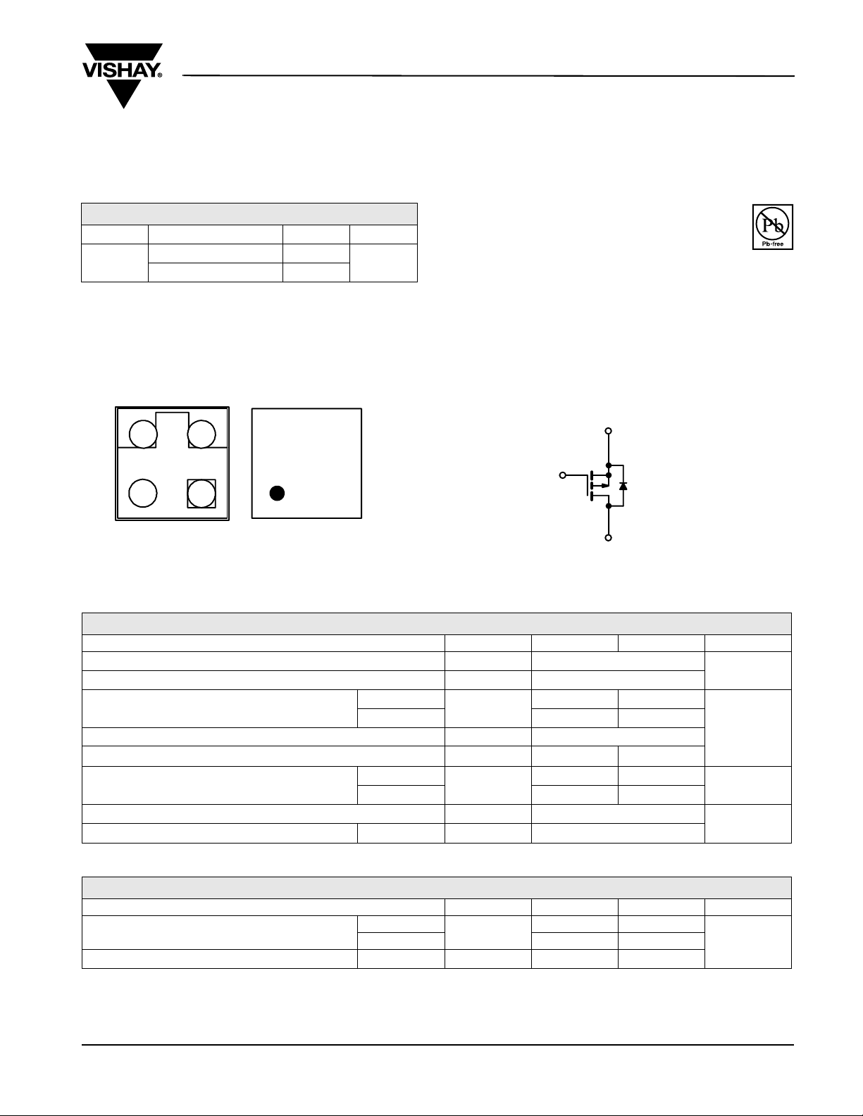
P-Channel 20-V (D-S) MOSFET
Si8413DB
Vishay Siliconix
PRODUCT SUMMARY
VDS (V) R
- 20
0.048 at V
0.063 at V
Bump Side View Backside View
32
DD
(Ω)I
DS(on)
= - 4.5 V
GS
= - 2.5 V
GS
MICRO FOOT
8413
D
- 6.5
- 5.7
xxx
S
41
Device Marking: 8413
Ordering Information: Si8413DB-T1-E1 (Lead (Pb)-free)
G
xxx = Date/Lot Traceability Code
(A) Qg (Typ.)
14
FEATURES
• TrenchFET® Power MOSFET
• MICRO FOOT
Reduces Footprint Area Profile (0.62 mm) and
On-Resistance Per Footprint Area
®
Chipscale Packaging
APPLICATIONS
• Load Switch
• Battery Switch
• Charger Switch
• PA Switch
S
G
D
P-Channel MOSFET
RoHS
COMPLIANT
ABSOLUTE MAXIMUM RATINGS TA = 25 °C, unless otherwise noted
Parameter Symbol 5 s Steady State Unit
Drain-Source Voltage
Gate-Source Voltage
Continuous Drain Current (T
= 150 °C)
J
a
Pulsed Drain Current
Continuous Source Current (Diode Conduction)
Maximum Power Dissipation
a
a
Operating Junction and Storage Temperature Range
Package Reflow Conditions
b
V
DS
V
GS
TA = 25 °C
= 70 °C
T
A
TA = 25 °C
= 70 °C
T
A
I
D
I
DM
I
S
P
D
T
, T
J
stg
- 6.5 - 4.8
- 5.2 - 3.8
- 2.5 - 1.3
2.77 1.47
1.77 0.94
IR/Convection 260
- 20
± 12
- 25
- 55 to 150
V
A
W
°C
THERMAL RESISTANCE RATINGS
Parameter Symbol Typical Maximum Unit
Maximum Junction-to-Ambient
a
t ≤ 5 s
Steady State 72 85
Maximum Junction-to-Foot (Drain) Steady State
Notes:
a. Surface Mounted on 1" x 1" FR4 board.
b. Refer to IPC/JEDEC (J-STD-020C), no manual or hand soldering.
R
thJA
R
thJF
35 45
°C/W
16 20
Document Number: 72947
S-82118-Rev. D, 08-Sep-08
www.vishay.com
1
Page 2
Si8413DB
Vishay Siliconix
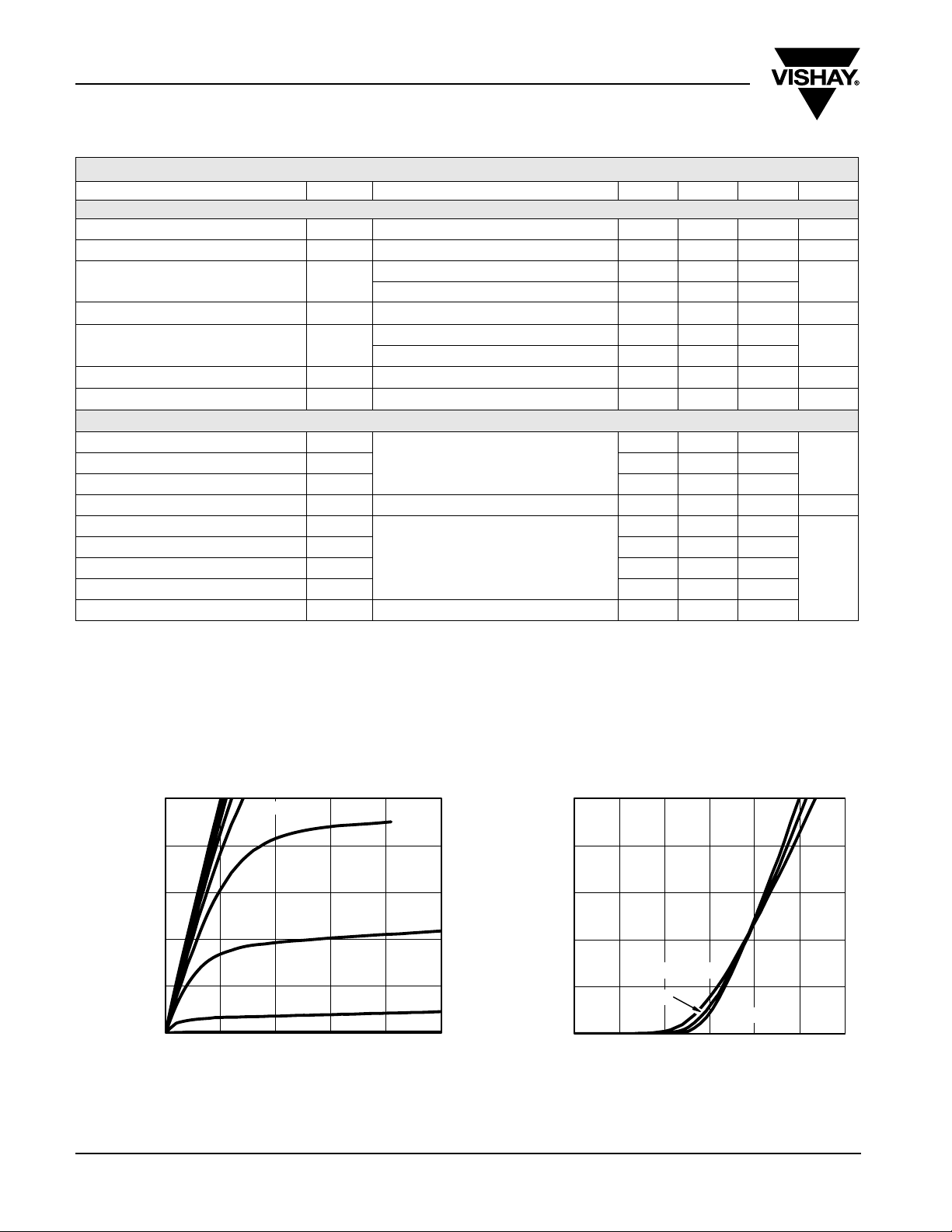
SPECIFICATIONS TJ = 25 °C, unless otherwise noted
Parameter Symbol Test Conditions Min. Typ. Max. Unit
Static
V
Gate Threshold Voltage
Gate-Body Leakage
Zero Gate Voltage Drain Current
On-State Drain Current
a
Drain-Source On-State Resistance
Forward Transconductance
Diode Forward Voltage
Dynamic
b
a
a
Total Gate Charge
Gate-Drain Charge
Gate Resistance
Tur n -O n De l ay Ti m e
Rise Time
Turn-Off Delay Time
Fall Time
Source-Drain Reverse Recovery Time
V
GS(th)
I
GSS
I
DSS
I
D(on)
a
R
DS(on)
g
fs
V
SD
Q
g
Q
gs
Q
gd
R
g
t
d(on)
t
r
t
d(off)
t
f
t
rr
V
V
V
DS
I
D
Notes:
a. Pulse test; pulse width ≤ 300 µs, duty cycle ≤ 2 %.
b. Guaranteed by design, not subject to production testing.
Stresses beyond those listed under “Absolute Maximum Ratings” may cause permanent damage to the device. These are stress ratings only, and functional operation
of the device at these or any other conditions beyond those indicated in the operational sections of the specifications is not implied. Exposure to absolute maximum
rating conditions for extended periods may affect device reliability.
= VGS, ID = - 250 µA
DS
VDS = 0 V, VGS = ± 12 V
V
= - 20 V, V
= - 20 V, V
DS
DS
V
V
DS
≤ - 5 V, V
= - 4.5 V, ID = - 1 A
GS
= - 2.5 V, ID = - 1 A
GS
GS
= 0 V, TJ = 70 °C
GS
= - 4.5 V
GS
VDS = - 10 V, ID = - 1 A
IS = - 1 A, V
= - 10 V, V
V
= - 10 V, RL = 10 Ω
DD
≅ - 1 A, V
GEN
= 0 V
GS
= - 4.5 V, ID = - 1 A
GS
= - 4.5 V, Rg = 6 Ω
IF = - 1 A, dI/dt = 100 A/µs
= 0 V
- 0.6 - 1.4 V
± 100 nA
- 1
- 5
µA
- 5 A
0.0393 0.048
0.052 0.063
7.4 S
- 0.8 - 1.1 V
14 21
1.7
nCGate-Source Charge
5.1
18 Ω
31 50
50 75
105 160
90 135
85 130
Ω
ns
TYPICAL CHARACTERISTICS 25 °C, unless otherwise noted
25
20
15
10
- Drain Current (A)
D
I
5
0
www.vishay.com
2
012345
VGS = 5 thru 3 V
V
- Drain-to-Source Voltage (V)
DS
Output Characteristics
2.5 V
2 V
1.5 V
- Drain Current (A)
D
I
25
20
15
10
5
0
0.0 0.5 1.0 1.5 2.0 2.5 3.0
TC = 125 °C
25 °C
- Gate-to-Source Voltage (V)
V
GS
- 55 °C
Transfer Characteristics
Document Number: 72947
S-82118-Rev. D, 08-Sep-08
Page 3
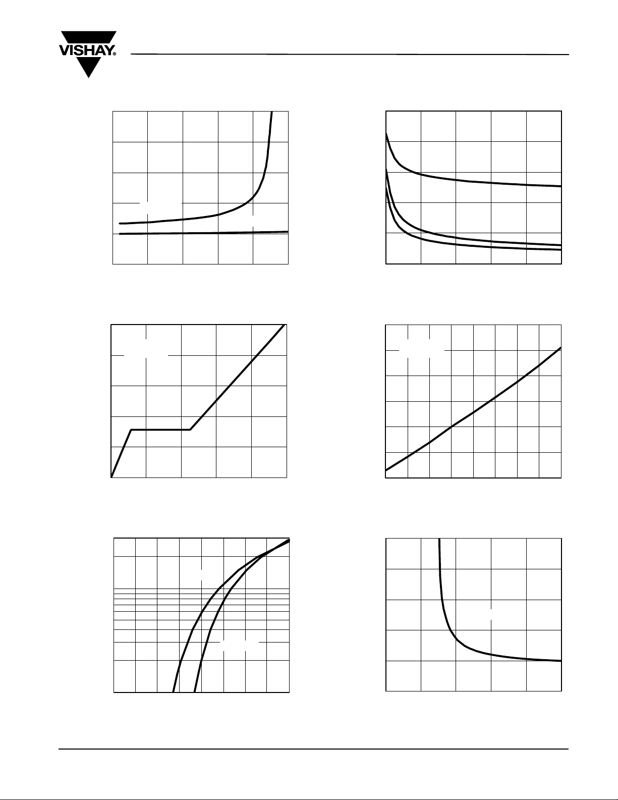
TYPICAL CHARACTERISTICS 25 °C, unless otherwise noted
Si8413DB
Vishay Siliconix
- On-Resistance (Ω)R
DS(on)
- Gate-to-Source Voltage (V)
GS
V
0.20
0.16
0.12
0.08
0.04
0.00
0 5 10 15 20 25
VGS = 2.5 V
VGS = 4.5 V
ID- Drain Current (A)
On-Resistance vs. Drain Current
5
VDS = 10 V
I
= 1 A
D
4
3
2
1
2000
1600
1200
800
C - Capacitance (pF)
400
0
048 12 16 20
1.4
1.3
1.2
1.1
On-Resistance
(Normalized)
1.0
DS(on)
R
0.9
C
iss
C
oss
C
rss
VDS- Drain-to-Source Voltage (V)
Capacitance
VGS = 4.5 V
I
= 1 A
D
0
03691215
30
10
Source Current (A)I
-
S
1
0.0 0.2 0.4 0.6 0.8 1.0 1.2 1.4 1.6
VSD- S o urce-to-Drain Voltage (V)
Source-Drain Diode Forward Voltage
Document Number: 72947
S-82118-Rev. D, 08-Sep-08
Qg- Total Gate Charge (nC)
Gate Charge
TJ = 150 °C
TJ = 25 °C
0.8
- 50 - 25 0 25 50 75 100 125 150
- Junction Temperature (°C)
T
J
On-Resistance vs. Junction Temperature
0.20
0.16
0.12
ID = 1 A
0.08
- On-Resistance (Ω)R
DS(on)
0.04
0.00
012345
VGS- Gate-to-Source Voltage (V)
On-Resistance vs. Gate-to-Source Voltage
www.vishay.com
3
Page 4
Si8413DB
Vishay Siliconix
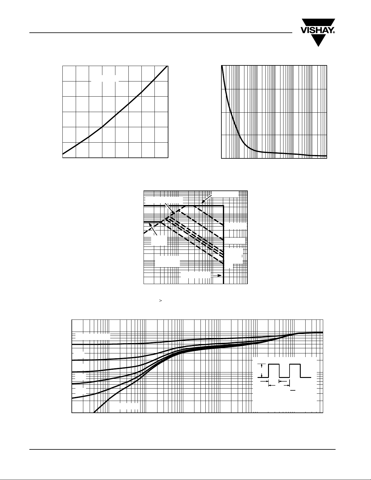
TYPICAL CHARACTERISTICS 25 °C, unless otherwise noted
0.4
0.3
ID = 250 µA
0.2
0.1
Variance (V)V
GS(th)
0.0
- 0.1
- 0.2
- 50 - 25 0 25 50 75 100 125 150
TJ- Temperature (°C)
Threshold Voltage
100
- Drain Current (A)I
D
0.01
80
60
40
Power (W)
20
0
0.001
0.01 0.1 1 100 600
Single Pulse Power, Junction-to-Ambient
Limited by R
DS(on)*
10
1
I
D(on)
Limited
0.1
TA = 25 °C
Single Pulse
BVDSS Limited
0.1 1 10 100
- Drain-to-Source Voltage (V)
V
DS
minimum VGS at which R
* V
GS
IDMLimited
is specified
DS(on)
P(t) = 0.001
P(t) = 0.01
P(t) = 0.1
P(t) = 1
P(t) = 10
DC
Safe Operating Area
10
Time (s)
Transient
Thermal Impedance
Normalized Effective
0.01
www.vishay.com
4
0.1
2
1
-4
10
Duty Cycle = 0.5
0.2
0.1
0.05
0.02
-3
10
Single Pulse
-2
10
-1
Square Wave Pulse Duration (s)
Normalized Thermal Transient Impedance, Junction-to-Ambient
Notes:
P
DM
t
1
t
- TA = PDMZ
JM
2
1. Duty Cycle, D =
2. Per Unit Base = R
3. T
4. Surface Mounted
Document Number: 72947
S-82118-Rev. D, 08-Sep-08
thJA
t
t
thJA
100
1
2
= 72 °C/W
(t)
00601110
Page 5
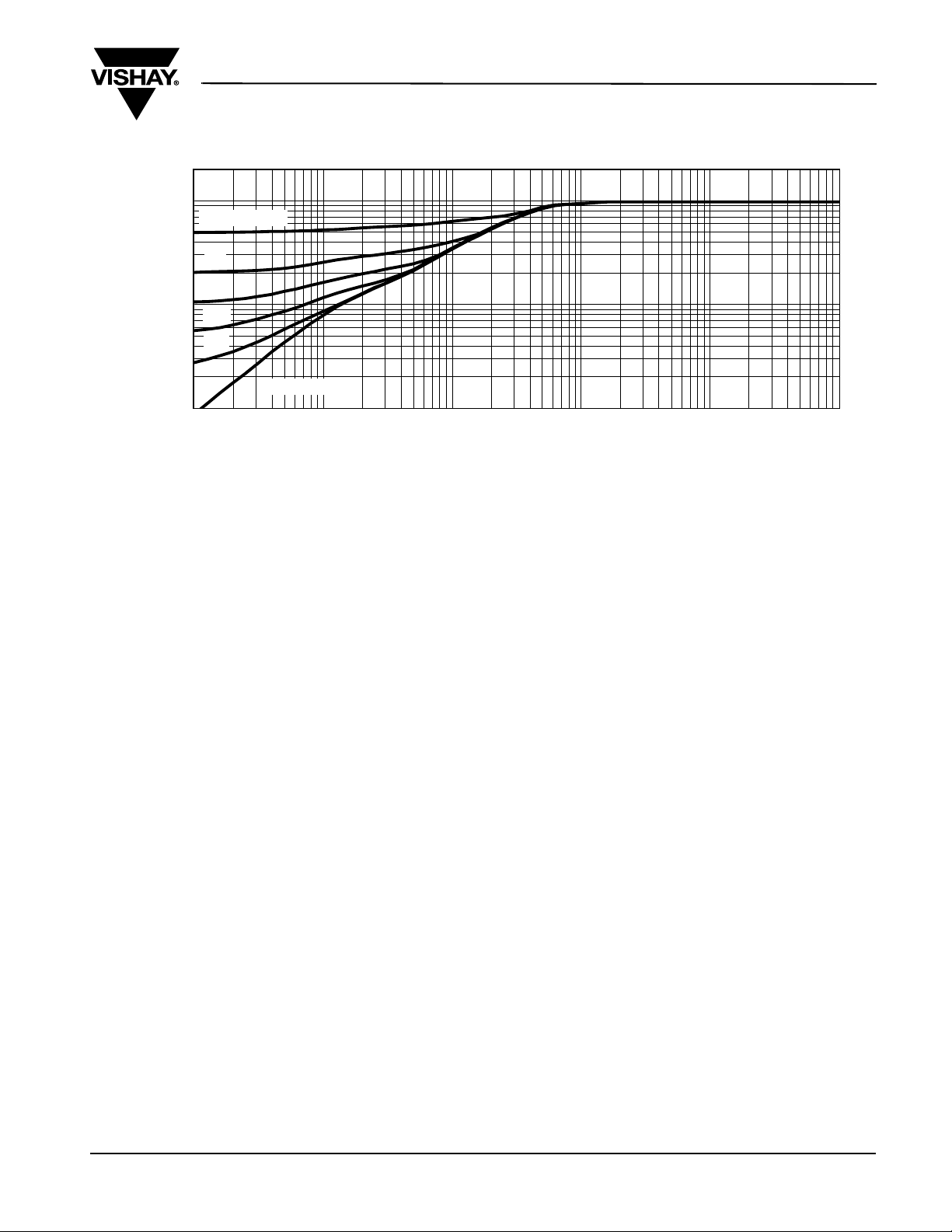
TYPICAL CHARACTERISTICS 25 °C, unless otherwise noted
2
1
Duty Cycle = 0.5
0.2
0.1
0.1
0.01
0.05
0.02
Single Pulse
-4
10
-3
10
-2
10
Square Wave Pulse Duration (s)
Normalized Thermal Transient Impedance, Junction-to-Foot
Thermal Impedance
Normalized Effective Transient
Si8413DB
Vishay Siliconix
-1
1
1010
Document Number: 72947
S-82118-Rev. D, 08-Sep-08
www.vishay.com
5
Page 6
Si8413DB
Vishay Siliconix
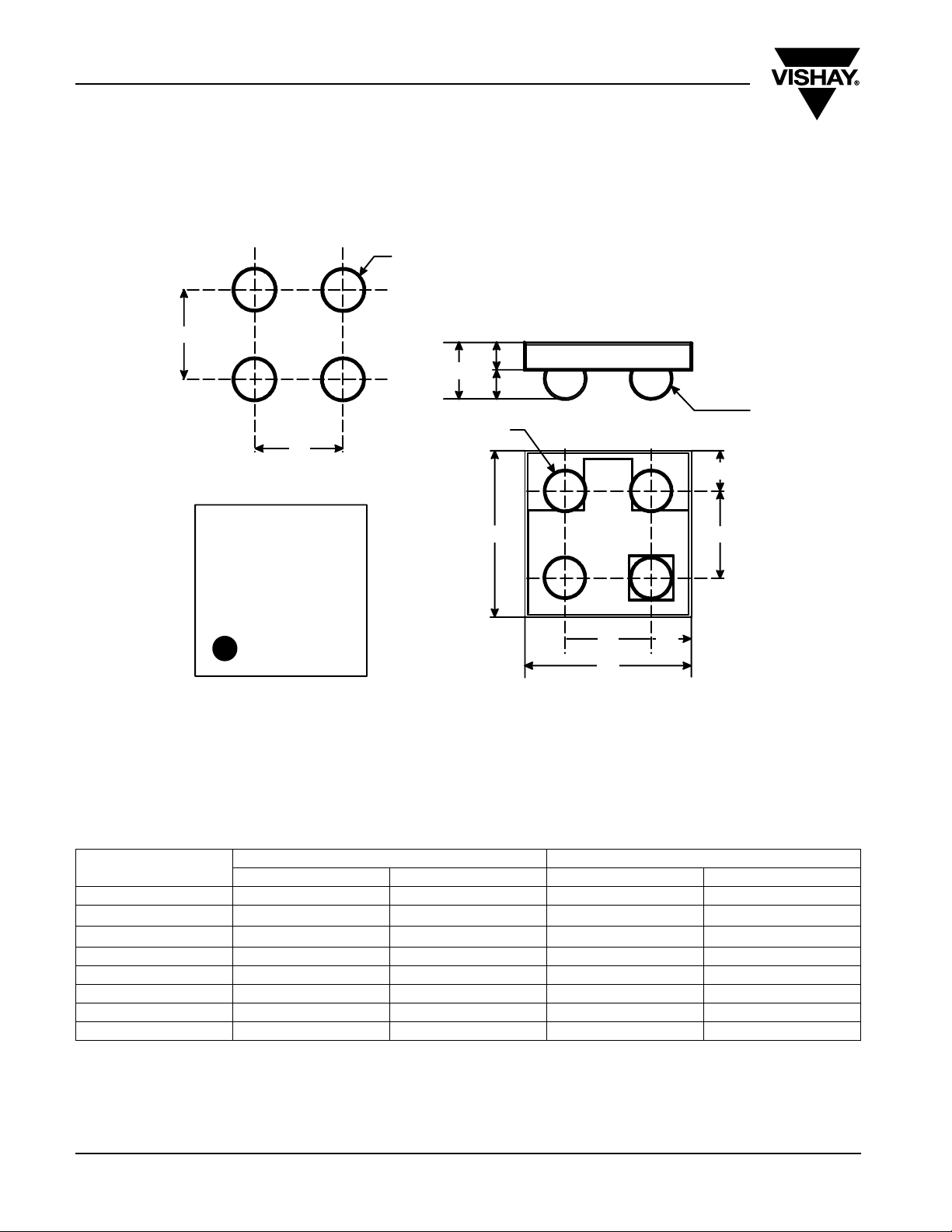
PACKAGE OUTLINE
MICRO FOOT: 4-BUMP (2 x 2, 0.8 mm PITCH)
e
Recommended Land
8413
XXX
Mark on Backside of Die
4 x φ 0.30 0.31
Note 3
Solder Mask φ 0.40
e
∼
∼
A
2
A
A
1
b Diamerter
Silicon
Bump Note 2
S
E
e S
D
e
Notes (Unless Otherwise Specified):
1. Laser mark on the silicon die back, coated with a thin metal.
2. Bumps are 95.5/3.8/0.7 Sn/Ag/Cu.
3. Non-solder mask defined copper landing pad.
4. The flat side of wafers is oriented at the bottom.
DIMENSIONS
Millimeters
MIN. MAX. MIN. MAX.
a
Inches
A 0.600 0.650 0.0236 0.0256
A
1
A
2
0.260 0.290 0.0102 0.0114
0.340 0.360 0.0134 0.0142
b 0.370 0.410 0.0146 0.0161
D 1.520 1.600 0.0598 0.0630
E 1.520 1.600 0.0598 0.0630
e 0.750 0.850 0.0295 0.0335
S 0.370 0.380 0.0146 0.0150
Notes:
a. Use millimeters as the primary measurement.
Vishay Siliconix maintains worldwide manufacturing capability. Products may be manufactured at one of several qualified locations. Reliability data for Silicon
Technology and Package Reliability represent a composite of all qualified locations. For related documents such as package/tape drawings, part marking, and
reliability data, see http://www.vishay.com/ppg?72947.
www.vishay.com
6
Document Number: 72947
S-82118-Rev. D, 08-Sep-08
Page 7
PCB Design and Assembly Guidelines
For MICRO FOOTr Products
Johnson Zhao
INTRODUCTION
Vishay Siliconix’s MICRO FOOT product family is based on a
wafer-level chip-scale packaging (WL-CSP) technology that
implements a solder bump process to eliminate the need for an
outer package to encase the silicon die. MICRO FOOT
products include power MOSFETs, analog switches, and
power ICs.
For battery powered compact devices, this new packaging
technology reduces board space requirements, improves
thermal performance, and mitigates the parasitic effect typical
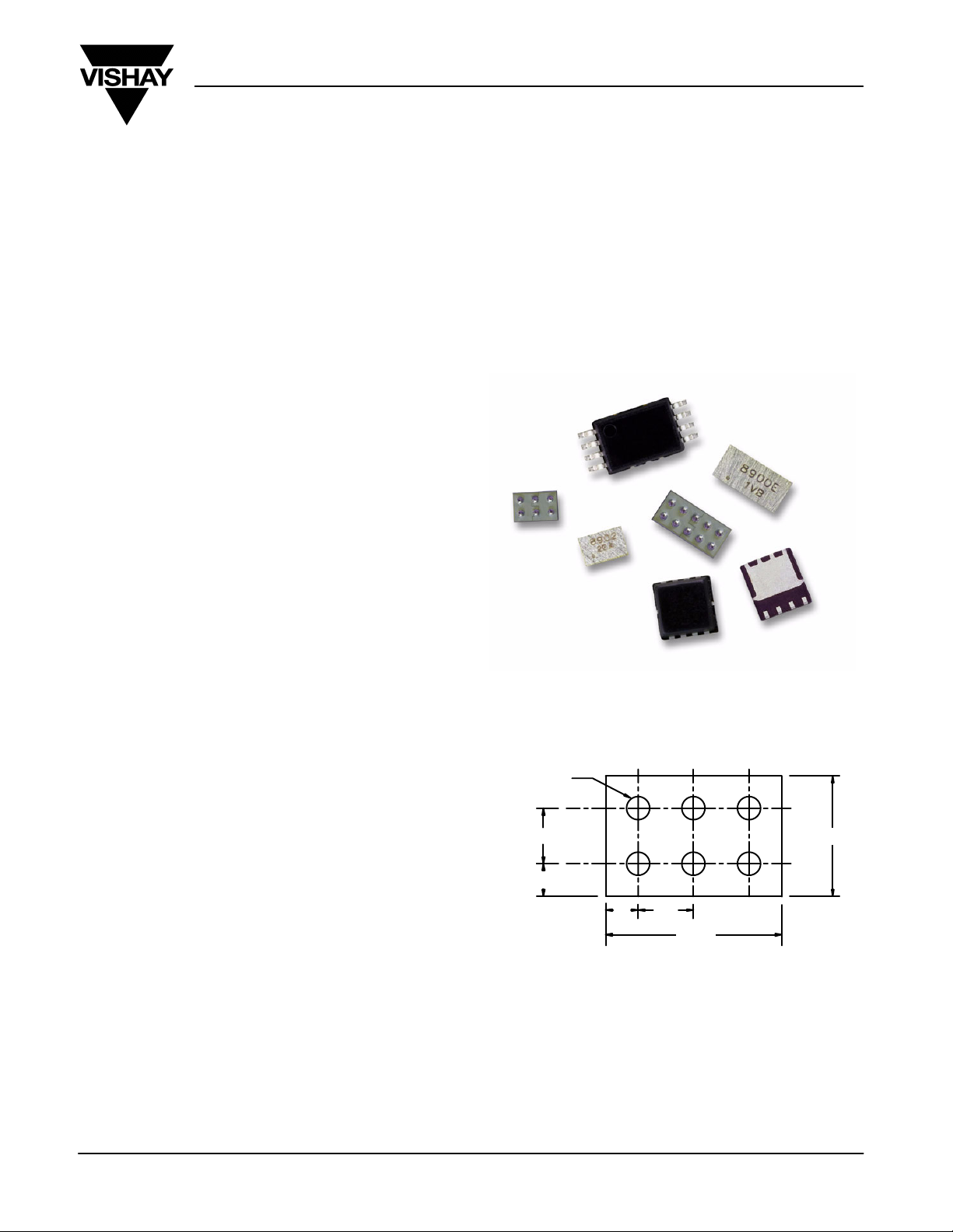
of leaded packaged products. For example, the 6−bump
MICRO FOOT Si8902EDB common drain power MOSFET,
which measures just 1.6 mm x 2.4 mm, achieves the same
performance as TSSOP−8 devices in a footprint that is 80%
smaller and with a 50% lower height profile (Figure 1). A
MICRO FOOT analog switch, the 6−bump DG3000DB, offers
low charge injection and 1.4 W on−resistance in a footprint
measuring just 1.08 mm x 1.58 mm (Figure 2).
AN824
Vishay Siliconix
Vishay Siliconix MICRO FOOT products can be handled with
the same process techniques used for high-volume assembly
of packaged surface-mount devices. With proper attention to
PCB and stencil design, the device will achieve reliable
performance without underfill. The advantage of the device’s
small footprint and short thermal path make it an ideal option
for space-constrained applications in portable devices such as
battery packs, PDAs, cellular phones, and notebook
computers.
This application note discusses the mechanical design and
reliability of MICRO FOOT, and then provides guidelines for
board layout, the assembly process, and the PCB rework
process.
FIGURE 1. 3D View of MICRO FOOT Products Si8902DB and
0.18 ~ 0.25
Si8900EDB
321
0.5
0.285
0.285
FIGURE 2. Outline of MICRO FOOT CSP & Analog
Switch DG3000DB
0.5
1.58
A
1.08
B
Document Number: 71990
06-Jan-03
www.vishay.com
1
Page 8
AN824
/
63Sm/37Pb
Vishay Siliconix
MICRO FOOT CSP
MICRO FOOT CSP MOSFET
MICRO FOOT CSP Analog Switch
MICRO FOOT UCSP Analog Switch
* All measurements in millimeters
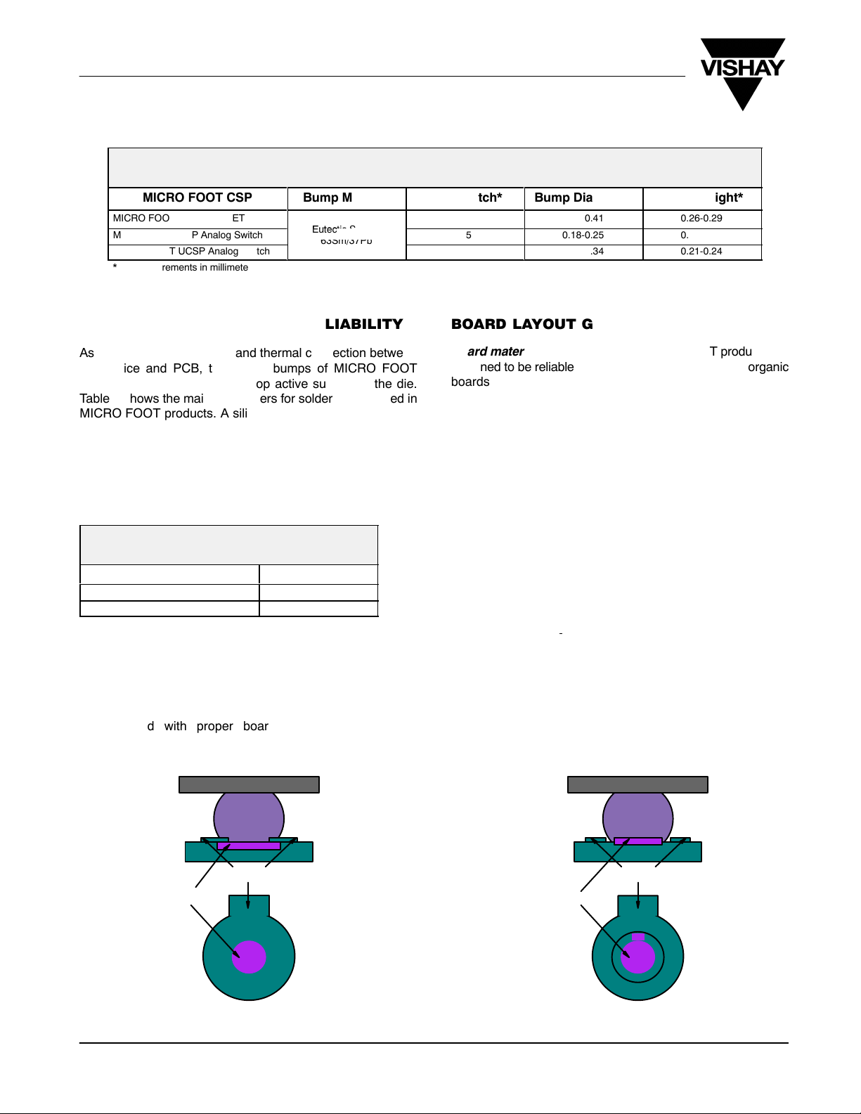
TABLE 1
Main Parameters of Solder Bumps in MICRO FOOT Designs
Bump Material
Eutectic Solder:
63Sm
37Pb
Bump Pitch*
0.8
0.5
0.5
Bump Diameter*
0.37-0.41
0.18-0.25
0.32-0.34
Bump Height*
0.26-0.29
0.14-0.19
0.21-0.24
MICRO FOOT’S DESIGN AND RELIABILITY
As a mechanical, electrical, and thermal connection between
the device and PCB, the solder bumps of MICRO FOOT
products are mounted on the top active surface of the die.
Table 1 shows the main parameters for solder bumps used in
MICRO FOOT products. A silicon nitride passivation layer is
applied to the active area as the last masking process in
fabrication,ensuring that the device passes the pressure pot
test. A green laser is used to mark the backside of the die
without damaging it. Reliability results for MICRO FOOT
products mounted on a FR-4 board without underfill are shown
in Table 2.
TABLE 2
MICRO FOOT Reliability Results
Test Condition C: −65_ to 150_C
Test condition B: −40_ to 125_C
121_C @ 15PSI 100% Humidity Test
The main failure mechanism associated with wafer-level
chip-scale packaging is fatigue of the solder joint. The results
shown in Table 2 demonstrate that a high level of reliability can
be achieved with proper board design and assembly
techniques.
>500 Cycles
>1000 Cycles
96 Hours
BOARD LAYOUT GUIDELINES
Board materials. Vishay Siliconix MICRO FOOT products are
designed to be reliable on most board types, including organic
boards such as FR-4 or polyamide boards. The package
qualification information is based on the test on 0.5-oz. FR-4
and polyamide boards with NSMD pad design.
Land patterns. Two types of land patterns are used for
surface-mount packages. Solder mask defined (SMD) pads
have a solder mask opening smaller than the metal pad
(Figure 3), whereas on-solder mask defined (NSMD) pads
have a metal pad smaller than the solder-mask opening
(Figure 4).
NSMD is recommended for copper etch processes, since it
provides a higher level of control compared to SMD etch
processes. A small-size NSMD pad definition provides more
area (both lateral and vertical) for soldering and more room for
escape routing on the PCB. By contrast, SMD pad definition
introduces a stress
on the PCB side that may result in solder joint cracking under
extreme fatigue conditions.
Copper pads should be finished with an organic solderability
preservative (OSP) coating. For electroplated
nickel-immersion gold finish pads, the gold thickness must be
less than 0.5 mm to avoid solder joint embrittlement.
concentration point near the solder mask
www.vishay.com
2
Solder Mask
Copper
FIGURE 3. SMD FIGURE 4. NSMD
Copper
Solder Mask
Document Number: 71990
06-Jan-03
Page 9
AN824
Á
Á
Á
Á
Vishay Siliconix
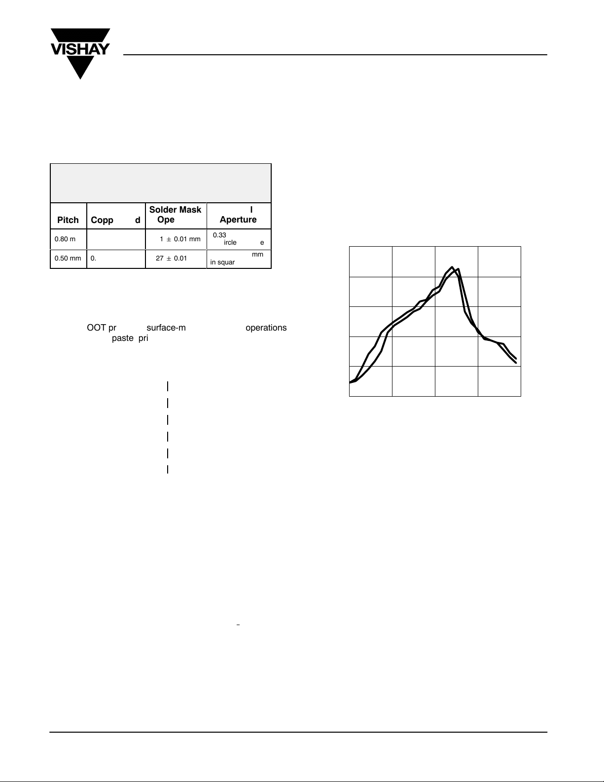
Board pad design. The landing-pad size for MICRO FOOT
products is determined by the bump pitch as shown in Table 3.
The pad pattern is circular to ensure a symmetric,
barrel-shaped solder bump.
TABLE 3
Dimensions of Copper Pad and Solder Mask
Opening in PCB and Stencil Aperture
Pitch
Á
0.80 mm
0.50 mm
Copper Pad
ÁÁÁ
0.30 " 0.01 mm
0.17 " 0.01 mm
Solder Mask
Opening
ÁÁÁ
0.41 " 0.01 mm
0.27 " 0.01 mm
Stencil
Aperture
ÁÁÁ
0.33 " 0.01 mm
in ciircle aperture
0.30 " 0.01 mm
in square aperture
ASSEMBLY PROCESS
MICRO FOOT products’ surface-mount-assembly operations
include solder paste printing, component placement, and
solder reflow as shown in the process flow chart (Figure 5).
Stencil Design
Chip pick-and-placement. MICRO FOOT products can be
picked and placed with standard pick-and-place equipment.
The recommended pick-and-place force is 150 g. Though the
part will self-center during solder reflow, the maximum
placement offset is 0.02 mm.
Reflow Process. MICRO FOOT products can be assembled
using standard SMT reflow processes. Similar to any other
package, the thermal profile at specific board locations must
be determined. Nitrogen purge is recommended during reflow
operation. Figure 6 shows a typical reflow profile.
Thermal Profile
250
200
150
100
Temperature (_C)
50
IIncoming Tape and Reel Inspection
Solder Paste Printing
Chip Placement
Reflow
Solder Joint Inspection
Pack and Ship
FIGURE 5. SMT Assembly Process Flow
Stencil design. Stencil design is the key to ensuring
maximum solder paste deposition without compromising the
assembly yield from solder joint defects (such as bridging and
extraneous solder spheres). The stencil aperture is dependent
on the copper pad size, the solder mask opening, and the
quantity of solder paste.
In MICRO FOOT products, the stencil is 0.125-
mm (5-mils)
thick. The recommended apertures are shown in Table 3 and
are fabricated by laser cut.
Solder-paste printing. The solder-paste printing process
involves transferring solder paste through pre-defined
apertures via application of pressure.
In MICRO FOOT products, the solder paste used is UP78
No-clean eutectic 63 Sn/37Pb type3 or finer solder paste.
0
0 100 200 300 400
Time (Seconds
FIGURE 6. Reflow Profile
PCB REWORK
To replace MICRO FOOT products on PCB, the rework
procedure is much like the rework process for a standard BGA
or CSP, as long as the rework process duplicates the original
reflow profile. The key steps are as follows:
1. Remove the MICRO FOOT device using a convection
nozzle to create localized heating similar to the original
reflow profile. Preheat from the bottom.
2. Once the nozzle temperature is +190_C, use tweezers to
remove the part to be replaced.
3. Resurface the pads using a temperature-controlled
soldering iron.
4. Apply gel flux to the pad.
5. Use a vacuum needle pick-up tip to pick up the
replacement part, and use a placement jig to placed it
accurately.
6. Reflow the part using the same convection nozzle, and
preheat from the bottom, matching the original reflow
profile.
Document Number: 71990
06-Jan-03
www.vishay.com
3
Page 10

Legal Disclaimer Notice
Vishay
Disclaimer
ALL PRODUCT, PRODUCT SPECIFICATIONS AND DATA ARE SUBJECT TO CHANGE WITHOUT NOTICE TO IMPROVE
RELIABILITY, FUNCTION OR DESIGN OR OTHERWISE.
Vishay Intertechnology, Inc., its affiliates, agents, and employees, and all persons acting on its or their behalf (collectively,
“Vishay”), disclaim any and all liability for any errors, inaccuracies or incompleteness contained in any datasheet or in any other
disclosure relating to any product.
Vishay makes no warranty, representation or guarantee regarding the suitability of the products for any particular purpose or
the continuing production of any product. To the maximum extent permitted by applicable law, Vishay disclaims (i) any and all
liability arising out of the application or use of any product, (ii) any and all liability, including without limitation special,
consequential or incidental damages, and (iii) any and all implied warranties, including warranties of fitness for particular
purpose, non-infringement and merchantability.
Statements regarding the suitability of products for certain types of applications are based on Vishay’s knowledge of typical
requirements that are often placed on Vishay products in generic applications. Such statements are not binding statements
about the suitability of products for a particular application. It is the customer’s responsibility to validate that a particular
product with the properties described in the product specification is suitable for use in a particular application. Parameters
provided in datasheets and/or specifications may vary in different applications and performance may vary over time. All
operating parameters, including typical parameters, must be validated for each customer application by the customer’s
technical experts. Product specifications do not expand or otherwise modify Vishay’s terms and conditions of purchase,
including but not limited to the warranty expressed therein.
Except as expressly indicated in writing, Vishay products are not designed for use in medical, life-saving, or life-sustaining
applications or for any other application in which the failure of the Vishay product could result in personal injury or death.
Customers using or selling Vishay products not expressly indicated for use in such applications do so at their own risk and agree
to fully indemnify and hold Vishay and its distributors harmless from and against any and all claims, liabilities, expenses and
damages arising or resulting in connection with such use or sale, including attorneys fees, even if such claim alleges that Vishay
or its distributor was negligent regarding the design or manufacture of the part. Please contact authorized Vishay personnel to
obtain written terms and conditions regarding products designed for such applications.
No license, express or implied, by estoppel or otherwise, to any intellectual property rights is granted by this document or by
any conduct of Vishay. Product names and markings noted herein may be trademarks of their respective owners.
Document Number: 91000 www.vishay.com
Revision: 11-Mar-11 1
 Loading...