

Page 1
Vishay Siliconix
N-Channel 30-V (D-S) Fast Switching MOSFET
Si7326DN
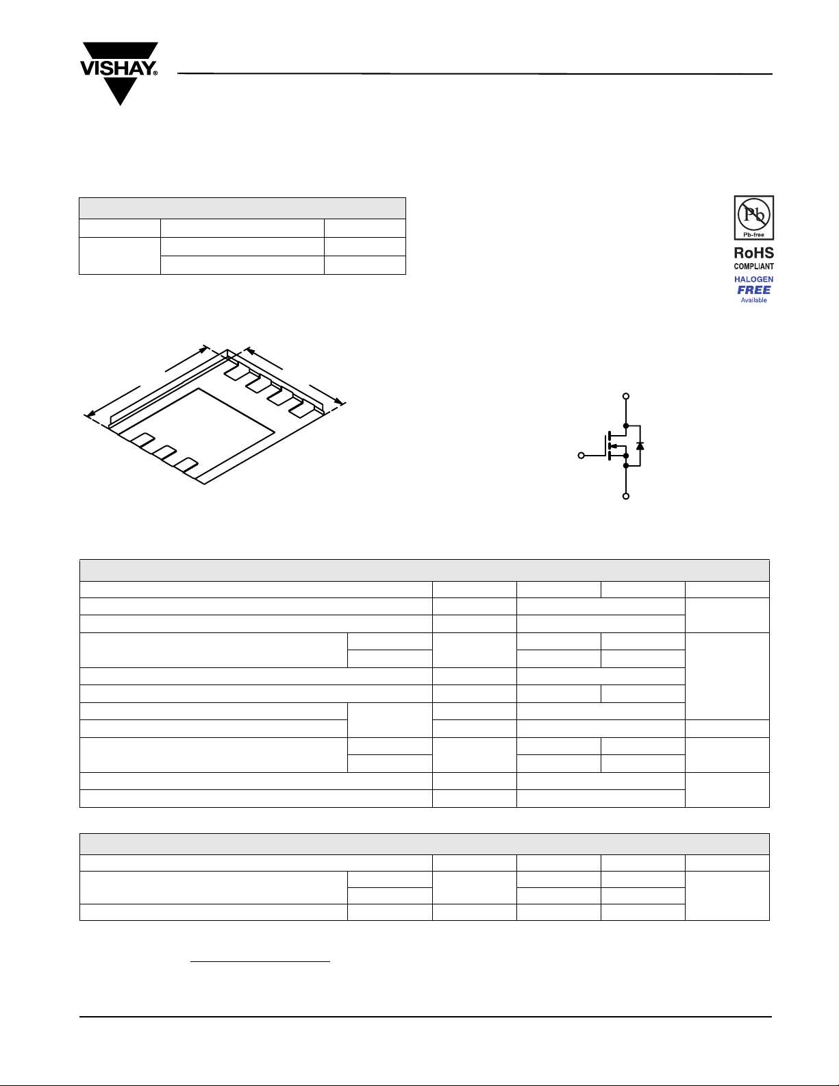
PRODUCT SUMMARY
VDS (V) R
30
DS(on)
0.0195 at V
0.030 at V
GS
(Ω)I
= 10 V
GS
= 4.5 V
D
(A)
10
8
FEATURES
• Halogen-free According to IEC 61249-2-21
Available
• TrenchFET
• New Low Thermal Resistance PowerPAK
®
Power MOSFET
®
Package with Low 1.07 mm Profile
PowerPAK 1212-8
• 100 % R
APPLICATIONS
Tested
g
• DC/DC Conversion
3.30 mm
D
8
D
7
D
6
5
Bottom View
Ordering Information: Si7326DN-T1-E3 (Lead (Pb)-free)
Si7326DN-T1-GE3 (Lead (Pb)-free and Halogen-free)
S
1
D
3.30 mm
S
2
S
3
G
4
G
N-Channel MOSFET
D
S
ABSOLUTE MAXIMUM RATINGS TA = 25 °C, unless otherwise noted
Parameter Symbol 10 s Steady State Unit
Drain-Source Voltage
Gate-Source Voltage
Continuous Drain Current (T
= 150 °C)
J
a
Pulsed Drain Current
Continuous Source Current (Diode Conduction)
a
Single Pulse Avalanche Current
Avalanche Energy
Maximum Power Dissipation
a
Operating Junction and Storage Temperature Range
Soldering Recommendations (Peak Temperature)
b, c
TA = 25 °C
= 70 °C
T
A
L = 0.1 mH
TA = 25 °C
= 70 °C
T
A
V
DS
V
GS
I
D
I
DM
I
S
I
AS
E
AS
P
D
, T
T
J
stg
10 6.5
7.5 5.0
2.9 1.2
3.5 1.5
1.9 0.8
30
± 25
40
15
11 mJ
- 55 to 150
260
V
A
W
°C
THERMAL RESISTANCE RATINGS
Parameter Symbol Typical Maximum Unit
Maximum Junction-to-Ambient
a
Maximum Junction-to-Case (Drain) Steady State
t ≤ 10 s
R
thJA
R
thJC
Notes:
a. Surface Mounted on 1" x 1" FR4 board.
b. See Solder Profile (www.vishay.com/ppg?73257
). The PowerPAK 1212-8 is a leadless package. The end of the lead terminal is exposed
copper (not plated) as a result of the singulation process in manufacturing. A solder fillet at the exposed copper tip cannot be guaranteed and
is not required to ensure adequate bottom side solder interconnection.
c. Rework Conditions: manual soldering with a soldering iron is not recommended for leadless components.
Document Number: 74444
S-83051-Rev. C, 29-Dec-08
28 35
°C/WSteady State 65 81
4.5 6.0
www.vishay.com
1
Page 2
Si7326DN
Vishay Siliconix
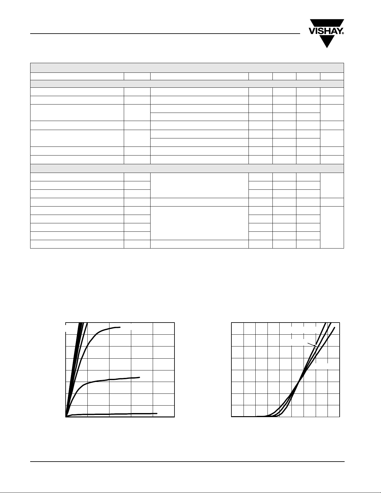
MOSFET SPECIFICATIONS TJ = 25 °C, unless otherwise noted
Parameter Symbol Test Conditions Min. Typ. Max. Unit
Static
V
Gate Threshold Voltage
Gate-Body Leakage
Zero Gate Voltage Drain Current
On-State Drain Current
Drain-Source On-State Resistance
Forward Transconductance
Diode Forward Voltage
Dynamic
b
a
a
a
a
Total Gate Charge
Gate-Drain Charge
Gate Resistance
Tur n -O n De l ay T i m e
Rise Time
Turn-Off Delay Time
Fall Time
Source-Drain Reverse Recovery Time
V
GS(th)
I
GSS
I
DSS
I
V
D(on)
R
DS(on)
g
fs
V
SD
Q
g
Q
gs
Q
gd
R
g
t
d(on)
t
r
t
d(off)
t
f
t
rr
V
V
Notes:
a. Pulse test; pulse width ≤ 300 µs, duty cycle ≤ 2 %.
b. Guaranteed by design, not subject to production testing.
Stresses beyond those listed under “Absolute Maximum Ratings” may cause permanent damage to the de vice. These are stress rating s only, and functiona l operation
of the device at these or any other conditions beyond those indicated in the operational sections of the specifications is not implied. Exposure to absolute maximum
rating conditions for extended periods may affect device reliability.
= VGS, ID = 250 µA
DS
VDS = 0 V, VGS = ± 20 V
V
= 30 V, V
DS
= 30 V, V
DS
GS
≥ 5 V, V
DS
V
= 10 V, ID = 10 A
GS
V
= 4.5 V, ID = 8 A
GS
= 0 V
GS
= 0 V, TJ = 55 °C
= 10 V
GS
VDS = 15 V, ID = 10 A
IS = 2.9 A, V
= 15 V, V
DS
V
= 15 V, RL = 15 Ω
DD
≅ 1 A, V
I
D
GEN
= 0 V
GS
= 5 V, ID = 10 A
GS
= 10 V, Rg = 6 Ω
IF = 2.9 A, dI/dt = 100 A/µs
0.8 1.8 V
± 100 nA
1
5
µA
30 A
0.015 0.0195
0.022 0.030
16 S
0.75 1.2 V
8.7 13
1.5
nCGate-Source Charge
3.5
0.5 1.4 2.2 Ω
815
12 20
32 50
14 25
30 60
Ω
ns
TYPICAL CHARACTERISTICS 25 °C, unless otherwise noted
40
VGS = 10 thru 5 V
35
30
25
20
15
Drain Current (A)I
-
D
10
5
0
www.vishay.com
2
012345
- Drain-to-Source Voltage (V)
V
DS
Output Characteristics
4 V
3 V
Drain Current (A)I
-
40
35
30
25
20
15
D
10
5
0
0.0 0.5 1.0 1.5 2.0 2.5 3.0 3.5 4.0 4.5
- Gate-to-Source Voltage (V)
V
GS
TC = - 55 °C
TC =
25 °C
Transfer Characteristics
Document Number: 74444
S-83051-Rev. C, 29-Dec-08
125 °C
=
T
C
Page 3
TYPICAL CHARACTERISTICS 25 °C, unless otherwise noted
0.040
Si7326DN
Vishay Siliconix
1200
- On-Resistance (Ω)R
DS(on)
Gate-to-Source Voltage (V)
-
V
0.032
0.024
0.016
0.008
0.000
0 5 10 15 20 25 30
VGS = 4.5 V
VGS = 10 V
ID- Drain Current (A)
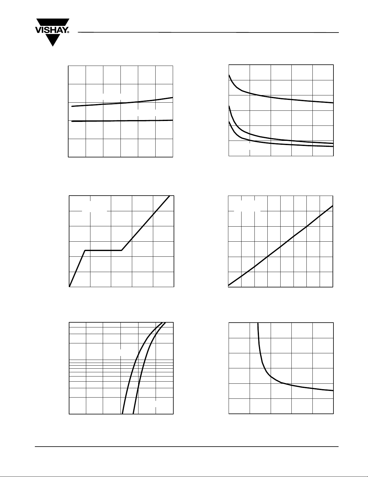
On-Resistance vs. Drain Current
6
VDS = 15 V
I
= 9 A
D
GS
5
4
3
2
1
1000
800
600
C - Capacitance (pF)
400
200
0
1.8
1.6
1.4
1.2
- On-Resistance
(Normalized)
1.0
DS(on)
R
0.8
C
iss
C
oss
C
rss
048121620
VDS - Drain-to-Source Voltage (V)
Capacitance
VGS = 10 V
I
= 9 A
D
0
0246810
50
10
Source Current (A)I
-
S
1
0.0 0.2 0.4 0.6 0.8 1.0 1.2
Source-Drain Diode Forward Voltage
Document Number: 74444
S-83051-Rev. C, 29-Dec-08
Qg - Total Gate Charge (nC)
Gate Charge
TJ = 150 °C
- Source-to-Drain Voltage (V)
V
SD
TJ = 25 °C
0.6
- 50 - 25 0 25 50 75 100 125 150
- Junction Temperature (°C)
T
J
On-Resistance vs. Junction Temperature
0.06
0.05
0.04
ID = 9 A
0.03
- On-Resistance (Ω)R
0.02
DS(on)
0.01
0.00
0246810
VGS- Gate-to-Source Voltage (V)
On-Resistance vs. Gate-to-Source Voltage
www.vishay.com
3
Page 4
Si7326DN
Vishay Siliconix
TYPICAL CHARACTERISTICS 25 °C, unless otherwise noted
0.4
50
0.2
ID = 250 µA
0.0
- 0.2
Variance (V)V
GS(th)
- 0.4
- 0.6
- 0.8
- 50 - 25 0 25 50 75 100 125 150
TJ- Temperature (°C)
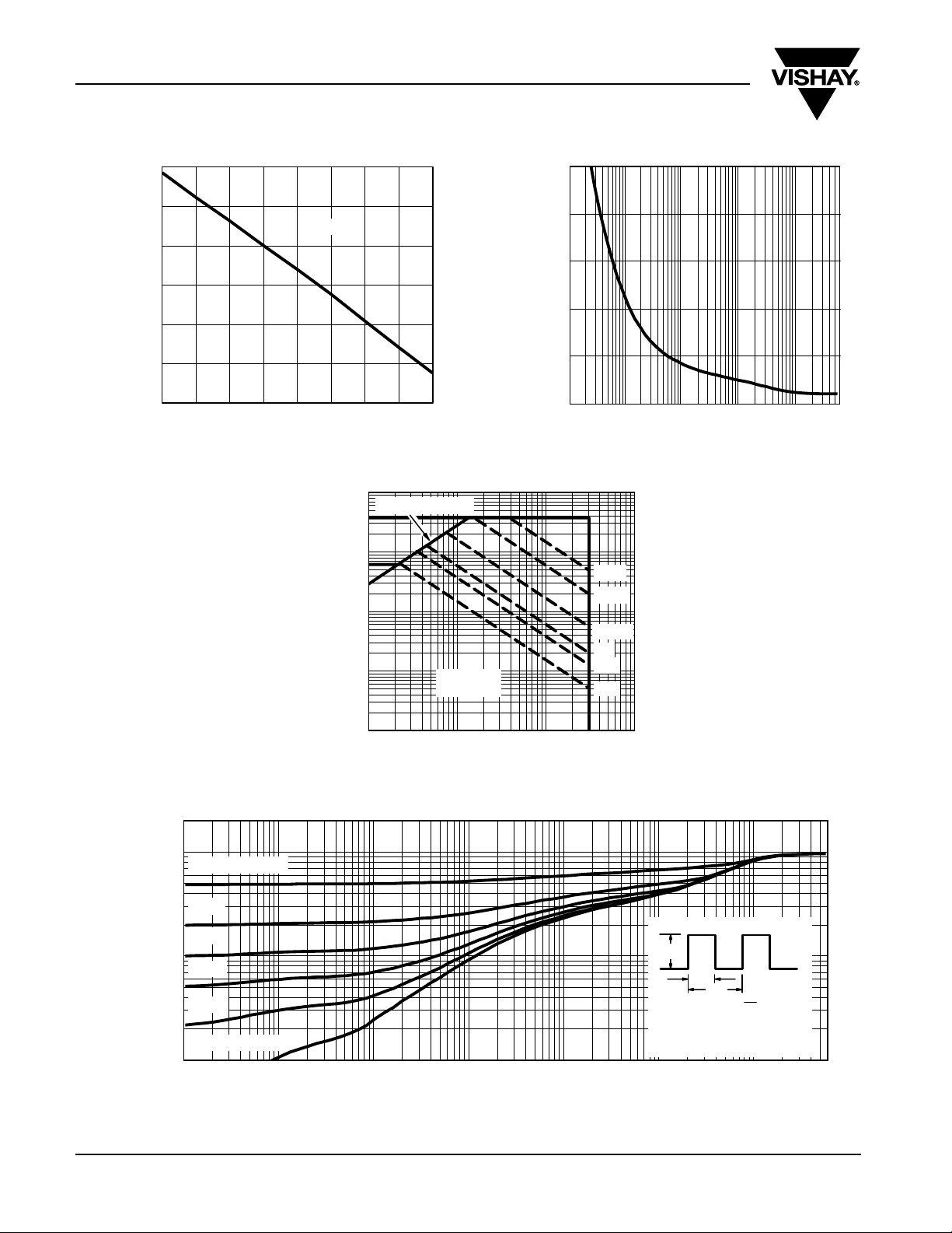
Threshold Voltage
100
10
1
Drain Current (A)I
-
D
0.1
Limited by R
*
DS(on)
TC = 25 °C
Single Pulse
Power (W)
40
30
20
10
0
0.01
0.1
1
10 100
Time (s)
Single Pulse Power, Junction-to-Ambient
1 ms
10 ms
100 ms
1 s
10 s
DC
600
Thermal Impedance
Normalized Effective Transient
0.01
www.vishay.com
4
0.1
2
1
-4
10
Duty Cycle = 0.5
0.2
0.1
0.05
0.02
Single Pulse
0.01
0.1 1 10 100
VDS- Drain-to-Source Voltage (V)
*V
> minimum VGSat which R
GS
DS(on)
is specified
Safe Operating Area, Junction-to-Foot
Notes:
P
DM
t
1
t
2
t
thJA
thJA
100
1
t
2
= 65 °C/W
(t)
1. Duty Cycle, D =
2. Per Unit Base = R
3. T
- TA = PDMZ
JM
4. Surface Mounted
-3
10
-2
10
-1
1 10 60010
Square Wave Pulse Duration (s)
Normalized Thermal Transient Impedance, Junction-to-Ambient
Document Number: 74444
S-83051-Rev. C, 29-Dec-08
Page 5
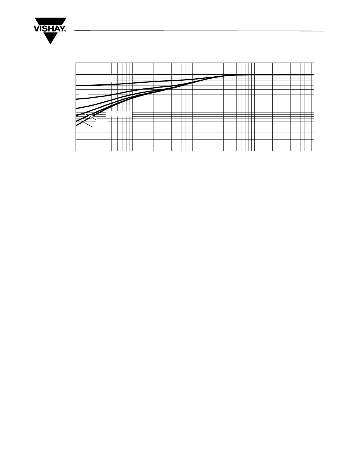
TYPICAL CHARACTERISTICS 25 °C, unless otherwise noted
2
1
Duty Cycle = 0.5
0.2
0.1
0.1
Thermal Impedance
Normalized Effective Transient
Single Pulse
0.05
0.02
Si7326DN
Vishay Siliconix
0.01
-4
10
-3
10
Square Wave Pulse Duration (s)
-2
10
-1
110
Normalized Thermal Transient Impedance, Junction-to-Case
Vishay Siliconix maintains worldwide manufacturing capability. Products may be manufactured at one of several qualified locations. Reliability data for Silicon
Technology and Package Reliability represent a composite of all qualified locations. For related documents such as package/tape drawings, part marking, and
reliability data, see www.vishay.com/ppg?74444
Document Number: 74444
.
www.vishay.com
S-83051-Rev. C, 29-Dec-08
5
Page 6
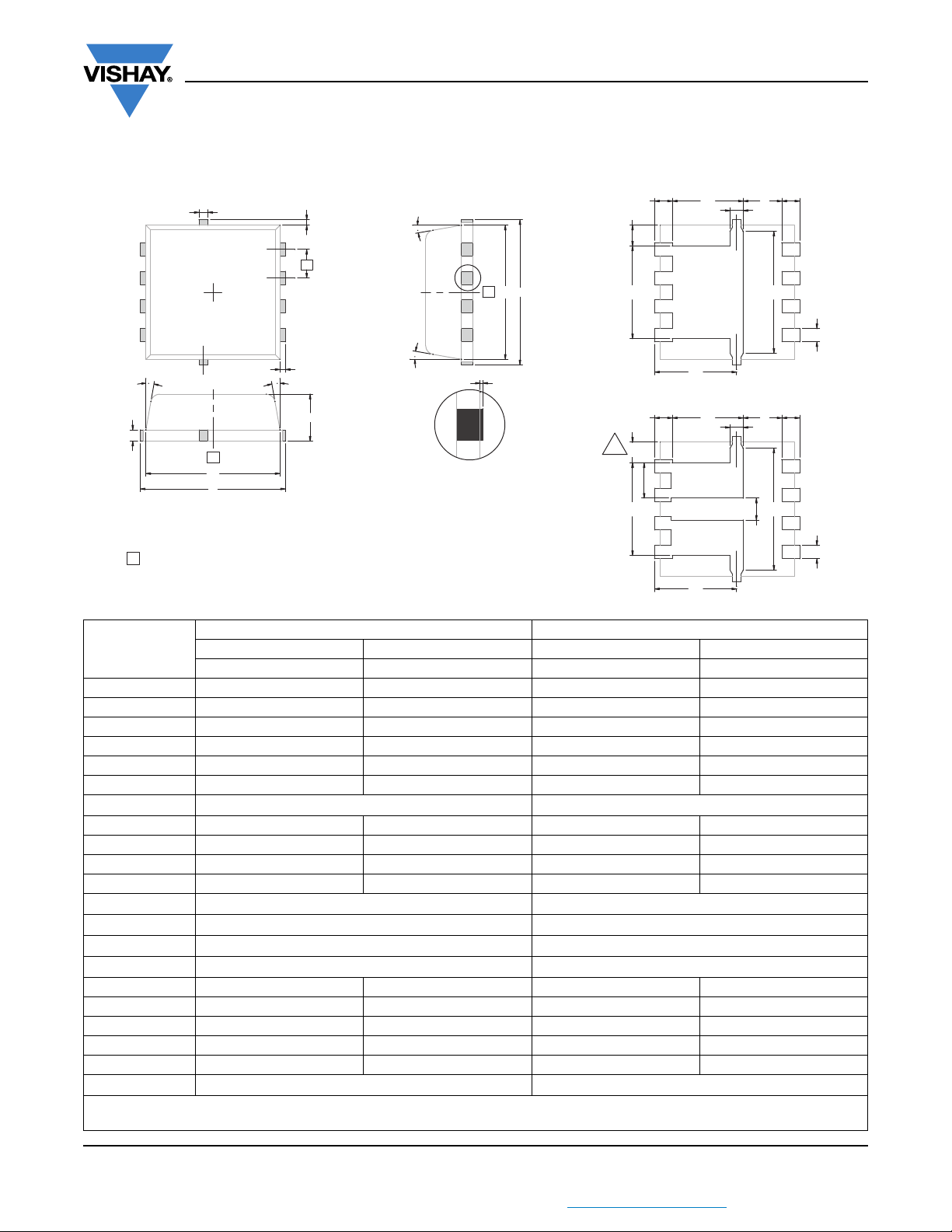
Package Information
www.vishay.com
Vishay Siliconix
PowerPAK® 1212, (Single/Dual)
L
W
M
1
8
e
θ
Z
2
D
D1
H
D4
D2
E2
E4
K
1
2
D5
3
45
θ
c
2
E1
E
Notes:
1.
Inch will govern
2
Dimensions exclusive of mold gate burrs
3.
Dimensions exclusive of mold flash and cutting burrs
DIM.
A 0.79 1.12 0.031 0.044
A1 0 0.05 0 0.002
b 0.23 0.41 0.009 0.016
c 0.13 0.33 0.005 0.013
D 3.00 3.61 0.118 0.142
D1 2.95 3.21 0.116 0.126
D2 1.98 2.70 0.078 0.106
D4
E 3.00 3.61 0.118 0.142
E1 2.95 3.21 0.116 0.126
E2 1.47 2.21 0.058 0.087
E3 1.75 1.98 0.069 0.078
E4
e
K
K1
H 0.15 0.51 0.006 0.020
L 0.15 0.56 0.006 0.022
L1 0.051 0.204 0.002 0.008
θ 0° 12° 0° 12°
W 0.15 0.36 0.006 0.014
M
ECN: C15-0077-Rev. K, 26-Jan-15
DWG: 5882
Revison: 26-Jan-15
L1
θ
A
θ
A1
Detail Z
Backside View of Single Pad
HK
H
D4
D3(2x)
D2
Backside View of Dual Pad
E3
E3
E2
D2
E4
D1
D5
K1
MILLIMETERS INCHES
MIN. MAX. MIN. MAX.
0.31 TYP. 0.012 TYP.
0.535 TYP. 0.021 TYP.
0.65 BSC 0.026 BSC
0.61 0.024
0.35 0.014
0.125 TYP. 0.005 TYP.
1
Document Number: 71656
4
b
L
1
2
3
b
4
THIS DOCUMENT IS SUBJECT TO CHANGE WITHOUT NOTICE. THE PRODUCTS DESCRIBED HEREIN AND THIS DOCUMENT
ARE SUBJECT TO SPECIFIC DISCLAIMERS, SET FORTH AT www.vishay.com/doc?91000
Page 7
PowerPAK® 1212 Mounting and Thermal Considerations
Johnson Zhao
AN822
Vishay Siliconix
MOSFETs for switching applications are now available
with die on resistances around 1 mΩ and with the
capability to handle 85 A. While these die capabilities
represent a major advance over what was available
just a few years ago, it is important for power MOSFET
packaging technology to keep pace. It should be obvious that degradation of a high performance die by the
package is undesirable.
technology that addresses these issues. The PowerPAK
1212-8 provides ultra-low thermal impedance in a
small package that is ideal for space-constrained
applications. In this application note, the PowerPAK
1212-8’s construction is described. Following this,
mounting information is presented. Finally, thermal
and electrical performance is discussed.
THE PowerPAK PACKAGE
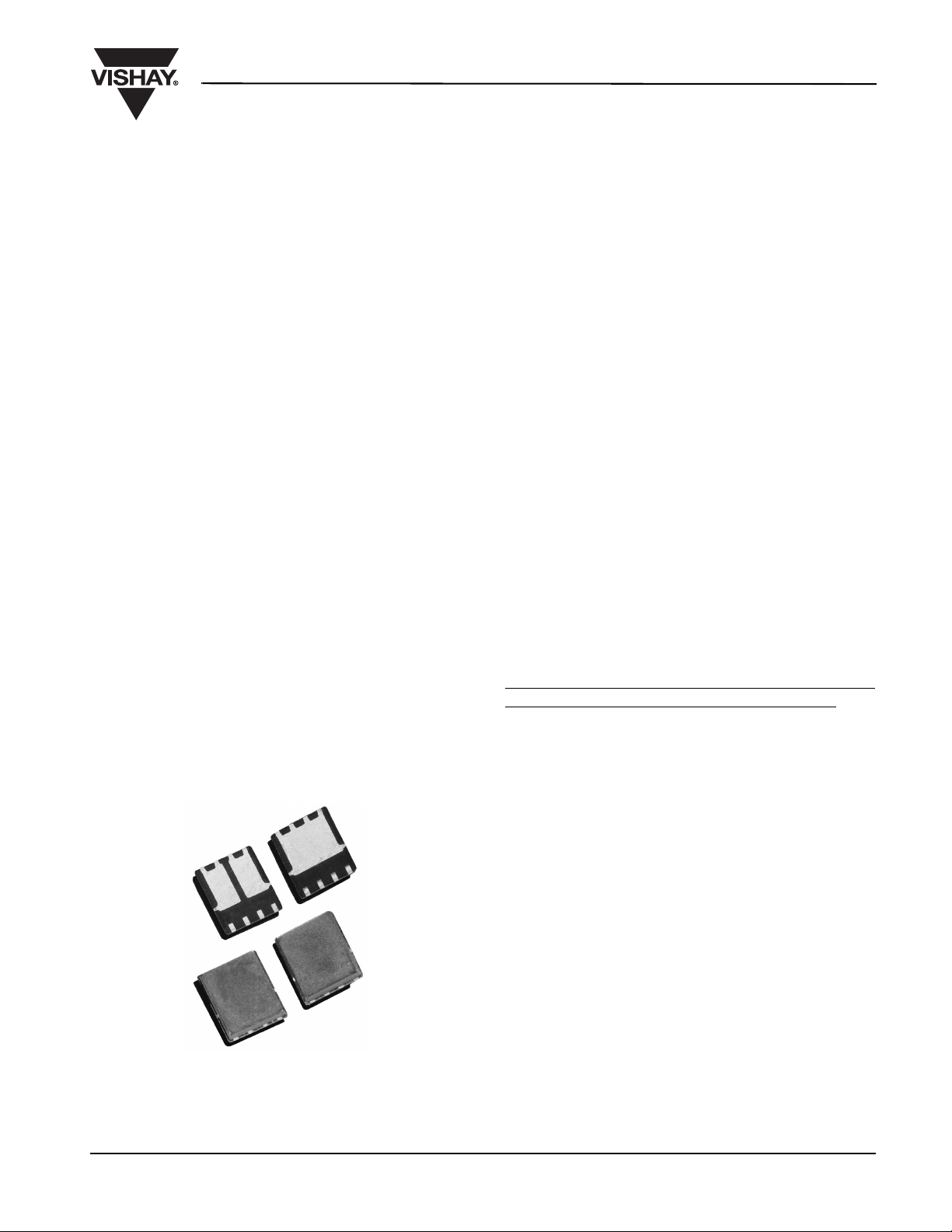
The PowerPAK 1212-8 package (Figure 1) is a derivative of PowerPAK SO-8. It utilizes the same packaging
technology, maximizing the die area. The bottom of the
die attach pad is exposed to provide a direct, low resistance thermal path to the substrate the device is
mounted on. The PowerPAK 1212-8 thus translates
the benefits of the PowerPAK SO-8 into a smaller
package, with the same level of thermal performance.
(Please refer to application note “PowerPAK SO-8
Mounting and Thermal Considerations.”)
PowerPAK is a new package
The PowerPAK 1212-8 has a footprint area comparable to TSOP-6. It is over 40 % smaller than standard
TSSOP-8. Its die capacity is more than twice the size
of the standard TSOP-6’s. It has thermal performance
an order of magnitude better than the SO-8, and 20
times better than TSSOP-8. Its thermal performance is
better than all current SMT packages in the market. It
will take the advantage of any PC board heat sink
capability. Bringing the junction temperature down also
increases the die efficiency by around 20 % compared
with TSSOP-8. For applications where bigger packages are typically required solely for thermal consideration, the PowerPAK 1212-8 is a good option.
Both the single and dual PowerPAK 1212-8 utilize the
same pin-outs as the single and dual PowerPAK SO-8.
The low 1.05 mm PowerPAK height profile makes both
versions an excellent choice for applications with
space constraints.
PowerPAK 1212 SINGLE MOUNTING
To take the advantage of the single PowerPAK 1212-8’s
thermal performance see Application Note 826,
Recommended Minimum Pad Patterns With Outline
Drawing Access for Vishay Siliconix MOSFETs. Click
on the PowerPAK 1212-8 single in the index of this
document.
In this figure, the drain land pattern is given to make full
contact to the drain pad on the PowerPAK package.
Figure 1. PowerPAK 1212 Devices
Document Number 71681
03-Mar-06
This land pattern can be extended to the left, right, and
top of the drawn pattern. This extension will serve to
increase the heat dissipation by decreasing the thermal resistance from the foot of the PowerPAK to the
PC board and therefore to the ambient. Note that
increasing the drain land area beyond a certain point
will yield little decrease in foot-to-board and foot-toambient thermal resistance. Under specific conditions
of board configuration, copper weight, and layer stack,
experiments have found that adding copper beyond an
area of about 0.3 to 0.5 in
ment in thermal performance.
2
of will yield little improve-
www.vishay.com
1
Page 8
AN822
Vishay Siliconix
PowerPAK 1212 DUAL
To take the advantage of the dual PowerPAK 1212-8’s
thermal performance, the minimum recommended
land pattern can be found in Application Note 826,
Recommended Minimum Pad Patterns With Outline
Drawing Access for Vishay Siliconix MOSFETs. Click
on the PowerPAK 1212-8 dual in the index of this document.
The gap between the two drain pads is 10 mils. This
matches the spacing of the two drain pads on the PowerPAK 1212-8 dual package.
This land pattern can be extended to the left, right, and
top of the drawn pattern. This extension will serve to
increase the heat dissipation by decreasing the thermal resistance from the foot of the PowerPAK to the
PC board and therefore to the ambient. Note that
increasing the drain land area beyond a certain point
will yield little decrease in foot-to-board and foot-toambient thermal resistance. Under specific conditions
of board configuration, copper weight, and layer stack,
experiments have found that adding copper beyond an
area of about 0.3 to 0.5 in
ment in thermal performance.
REFLOW SOLDERING
Vishay Siliconix surface-mount packages meet solder
reflow reliability requirements. Devices are subjected
to solder reflow as a preconditioning test and are then
reliability-tested using temperature cycle, bias humidity, HAST, or pressure pot. The solder reflow tempera-
2
of will yield little improve-
ture profile used, and the temperatures and time
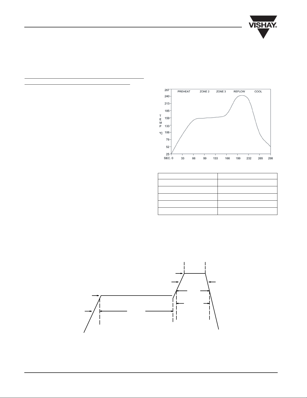
duration, are shown in Figures 2 and 3. For the lead
(Pb)-free solder profile, see http://www.vishay.com/
doc?73257.
Ramp-Up Rate + 6 °C /Second Maximum
Temperature at 155 ± 15 °C 120 Seconds Maximum
Temperature Above 180 °C 70 - 180 Seconds
Maximum Temperature
Time at Maximum Temperature
Ramp-Down Rate
Figure 2. Solder Reflow Temperature Profile
240 + 5/- 0 °C
20 - 40 Seconds
+ 6 °C/Second Maximum
www.vishay.com
2
140 - 170 °C
3° C/s (max)
10 s (max)
210 - 220 °C
3 °C/s (max) 4 °C/s (max)
183 °C
50 s (max)
60 s (min)
Pre-Heating Zone
Maximum peak temperature at 240 °C is allowed.
Figure 3. Solder Reflow Temperatures and Time Durations
Reflow Zone
Document Number 71681
03-Mar-06
Page 9
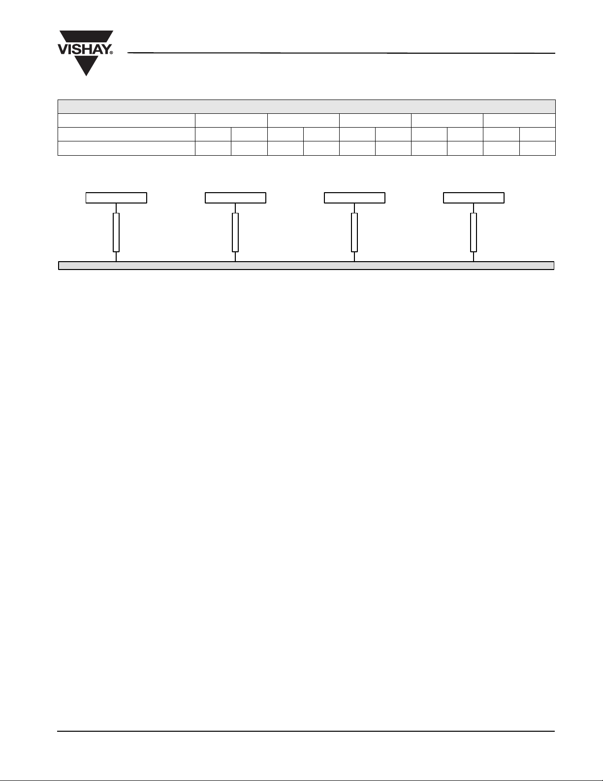
TABLE 1: EQIVALENT STEADY STATE PERFORMANCE
Package SO-8 TSSOP-8 TSOP-8 PPAK 1212 PPAK SO-8
Configuration Single Dual Single Dual Single Dual Single Dual Single Dual
Thermal Resiatance R
thJC
(C/W)
20 40 52 83 40 90 2.4 5.5 1.8 5.5
AN822
Vishay Siliconix
PowerPAK 1212
49.8 °C
2.4 °C/W
PC Board at 45 °C
Standard SO-8
85 °C
20 °C/W
Figure 4. Temperature of Devices on a PC Board
THERMAL PERFORMANCE
Introduction
A basic measure of a device’s thermal performance is
the junction-to-case thermal resistance, Rθjc, or the
junction to- foot thermal resistance, Rθjf. This parameter
is measured for the device mounted to an infinite heat
sink and is therefore a characterization of the device
only, in other words, independent of the properties of the
object to which the device is mounted. Table 1 shows a
comparison of the PowerPAK 1212-8, PowerPAK SO-8,
standard TSSOP-8 and SO-8 equivalent steady state
performance.
By minimizing the junction-to-foot thermal resistance, the
MOSFET die temperature is very close to the temperature of the PC board. Consider four devices mounted on
a PC board with a board temperature of 45 °C (Figure 4)
Suppose each device is dissipating 2 W. Using the junction-to-foot thermal resistance characteristics of the
PowerPAK 1212-8 and the other SMT packages, die
temperatures are determined to be 49.8 °C for the PowerPAK 1212-8, 85 °C for the standard SO-8, 149 °C for
standard TSSOP-8, and 125 °C for TSOP-6. This is a
4.8 °C rise above the board temperature for the PowerPAK 1212-8, and over 40 °C for other SMT packages. A
4.8 °C rise has minimal effect on r
of over 40 °C will cause an increase in r
whereas a rise
DS(ON)
DS(ON)
as high
as 20 %.
Standard TSSOP-8
149 °C
52 °C/W
TSOP-6
40 °C/W
Spreading Copper
Designers add additional copper, spreading copper, to
the drain pad to aid in conducting heat from a device. It
is helpful to have some information about the thermal
performance for a given area of spreading copper.
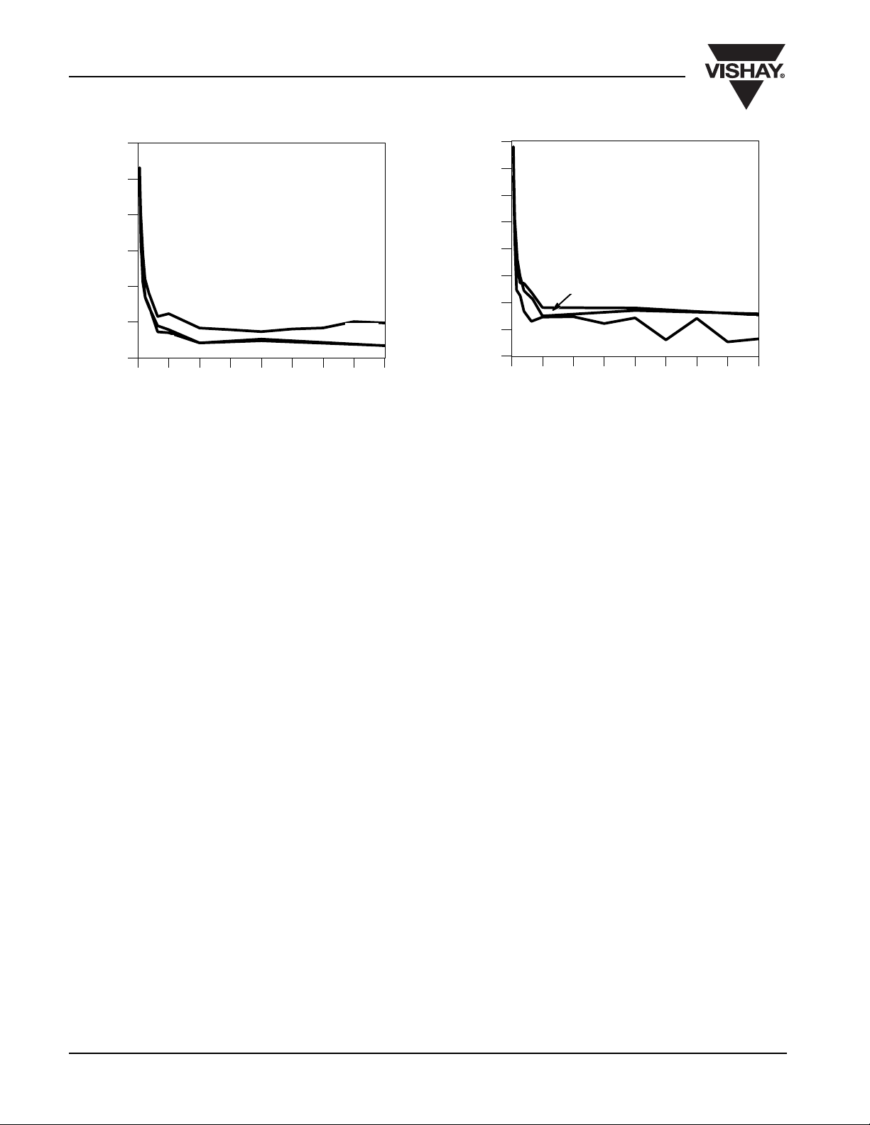
Figure 5 and Figure 6 show the thermal resistance of a
PowerPAK 1212-8 single and dual devices mounted on
a 2-in. x 2-in., four-layer FR-4 PC boards. The two internal layers and the backside layer are solid copper. The
internal layers were chosen as solid copper to model the
large power and ground planes common in many applications. The top layer was cut back to a smaller area and
at each step junction-to-ambient thermal resistance
measurements were taken. The results indicate that an
area above 0.2 to 0.3 square inches of spreading copper
.
gives no additional thermal performance improvement.
A subsequent experiment was run where the copper on
the back-side was reduced, first to 50 % in stripes to
mimic circuit traces, and then totally removed. No significant effect was observed.
125 °C
Document Number 71681
03-Mar-06
www.vishay.com
3
Page 10
AN822
Vishay Siliconix
105
95
85
75
(°C/W)
AJht
R
65
55
45
Spreading Copper (sq. in.)
100 %
50 %
0 %
0.00 0.25 0.50 0.75 1.00 1.25 1.50 1.75 2.00
Figure 5. Spreading Copper - Si7401DN
CONCLUSIONS
As a derivative of the PowerPAK SO-8, the PowerPAK
1212-8 uses the same packaging technology and has
been shown to have the same level of thermal performance while having a footprint that is more than 40 %
smaller than the standard TSSOP-8.
Recommended PowerPAK 1212-8 land patterns are
provided to aid in PC board layout for designs using this
new package.
130
120
110
100
(°C/W)
AJ
ht
R
Figure 6. Spreading Copper - Junction-to-Ambient Performance
Spreading Copper (sq. in.)
90
80
70
60
50
0.00 0.25 0.50 0.75 1.00 1.25 1.50 1.75 2.00
50 %
100 %
0 %
The PowerPAK 1212-8 combines small size with attractive thermal characteristics. By minimizing the thermal
rise above the board temperature, PowerPAK simplifies
thermal design considerations, allows the device to run
cooler, keeps r
low, and permits the device to
DS(ON)
handle more current than a same- or larger-size MOSFET die in the standard TSSOP-8 or SO-8 packages.
www.vishay.com
4
Document Number 71681
03-Mar-06
Page 11
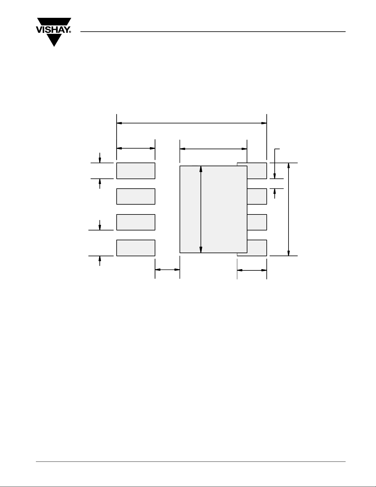
RECOMMENDED MINIMUM PADS FOR PowerPAK® 1212-8 Single
0.152
(3.860)
Application Note 826
Vishay Siliconix
0.016
(0.405)
0.026
(0.660)
Return to Index
0.039
(0.990)
0.068
(1.725)
0.088
(2.235)
0.025
(0.635)
Recommended Minimum Pads
Dimensions in Inches/(mm)
0.030
(0.760)
0.010
(0.255)
0.094
(2.390)
Return to Index
Document Number: 72597 www.vishay.com
Revision: 21-Jan-08 7
APPLICATION NOTE
Page 12

Legal Disclaimer Notice
www.vishay.com
Vishay
Disclaimer
ALL PRODUCT, PRODUCT SPECIFICATIONS AND DATA ARE SUBJECT TO CHANGE WITHOUT NOTICE TO IMPROVE
RELIABILITY, FUNCTION OR DESIGN OR OTHERWISE.
Vishay Intertechnology, Inc., its affiliates, agents, and employees, and all persons acting on its or their behalf (collectively,
“Vishay”), disclaim any and all liability for any errors, inaccuracies or incompleteness contained in any datasheet or in any other
disclosure relating to any product.
Vishay makes no warranty, representation or guarantee regarding the suitability of the products for any particular purpose or
the continuing production of any product. To the maximum extent permitted by applicable law, Vishay disclaims (i) any and all
liability arising out of the application or use of any product, (ii) any and all liability, including without limitation special,
consequential or incidental damages, and (iii) any and all implied warranties, including warranties of fitness for particular
purpose, non-infringement and merchantability.
Statements regarding the suitability of products for certain types of applications are based on Vishay’s knowledge of typical
requirements that are often placed on Vishay products in generic applications. Such statements are not binding statements
about the suitability of products for a particular application. It is the customer’s responsibility to validate that a particular
product with the properties described in the product specification is suitable for use in a particular application. Parameters
provided in datasheets and/or specifications may vary in different applications and performance may vary over time. All
operating parameters, including typical parameters, must be validated for each customer application by the customer’s
technical experts. Product specifications do not expand or otherwise modify Vishay’s terms and conditions of purchase,
including but not limited to the warranty expressed therein.
Except as expressly indicated in writing, Vishay products are not designed for use in medical, life-saving, or life-sustaining
applications or for any other application in which the failure of the Vishay product could result in personal injury or death.
Customers using or selling Vishay products not expressly indicated for use in such applications do so at their own risk. Please
contact authorized Vishay personnel to obtain written terms and conditions regarding products designed for such applications.
No license, express or implied, by estoppel or otherwise, to any intellectual property rights is granted by this document or by
any conduct of Vishay. Product names and markings noted herein may be trademarks of their respective owners.
Material Category Policy
Vishay Intertechnology, Inc. hereby certifies that all its products that are identified as RoHS-Compliant fulfill the
definitions and restrictions defined under Directive 2011/65/EU of The European Parliament and of the Council
of June 8, 2011 on the restriction of the use of certain hazardous substances in electrical and electronic equipment
(EEE) - recast, unless otherwise specified as non-compliant.
Please note that some Vishay documentation may still make reference to RoHS Directive 2002/95/EC. We confirm that
all the products identified as being compliant to Directive 2002/95/EC conform to Directive 2011/65/EU.
Vishay Intertechnology, Inc. hereby certifies that all its products that are identified as Halogen-Free follow Halogen-Free
requirements as per JEDEC JS709A standards. Please note that some Vishay documentation may still make reference
to the IEC 61249-2-21 definition. We confirm that all the products identified as being compliant to IEC 61249-2-21
conform to JEDEC JS709A standards.
Revision: 02-Oct-12
1
Document Number: 91000
Page 13

 Loading...