

Page 1
Bottom View
PRELIMINARY DATA SHEET
SiPHY™ OC-192/STM-64 TRANSMITTER
Features
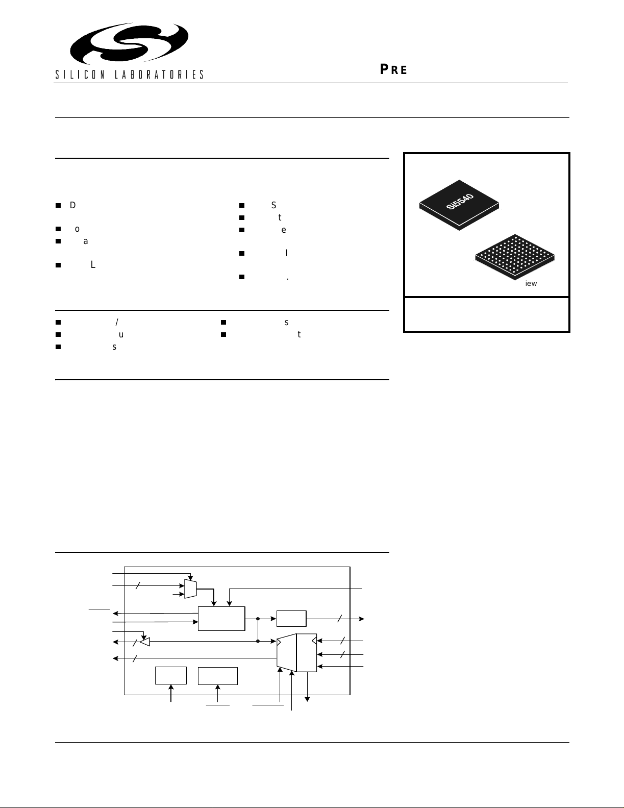
Si5540
Complete SONET/SDH transmitter for OC-192/STM-64 data rates with integrated
16:1 multiplexer and DSPLL
Data Rates Supported: OC-192/STM-64,
10GbE, and 10.7 Gbps FEC
Low Power Operation 0.6 W (typ)
Small Footprint: 99-Pin BGA Package
(11 x 11mm)
DSPLL™ Based Clock Multiplier Unit
w/ selectable loop filter bandwidths
™
based clock multiplier unit:
OIF SFI-4 Compliant Interface
Output Clock Powerdown
Operates with 155 or 622 MHz
Reference Sources
Optional 3.3 V Supply Pin for
LVTTL Compatible Outputs
Single 1.8 V Supply Operation
Applications
Sonet/SDH/ATM Routers
Add/Drop Multiplexers
Digital Cross Connects
Optical Transceiver Modules
Sone t / S D H Test E qu ipm en t
Description
The Si5540 is a fully integrated low-power transmitter for high-speed serial
communication systems. It combines high speed clock generation with a 16:1
multiplexer to serialize data for OC-192/STM-64 applications. The Si5540 is based
on Silicon Laboratories’ DSPLL
filter components required by traditional clock multiplier units. In addition,
selectable loop filter bandwidths are provided to ensure superior jitter performance
while relaxing the jitter requirements on external clock distribution subsystems.
Support for data streams up to 10.7 G bps is also provided for applications that
employ forward error correction (FEC).
The Si5540 represents a new standard in low jitter, low power and small size for
10 Gbps serial transmitters. It operates from a single 1.8 V supply over the
industrial t em perature range (–40°C to 85°C).
™
technology which eliminates the external loop
Si5364
Ordering Information:
See pa ge17.
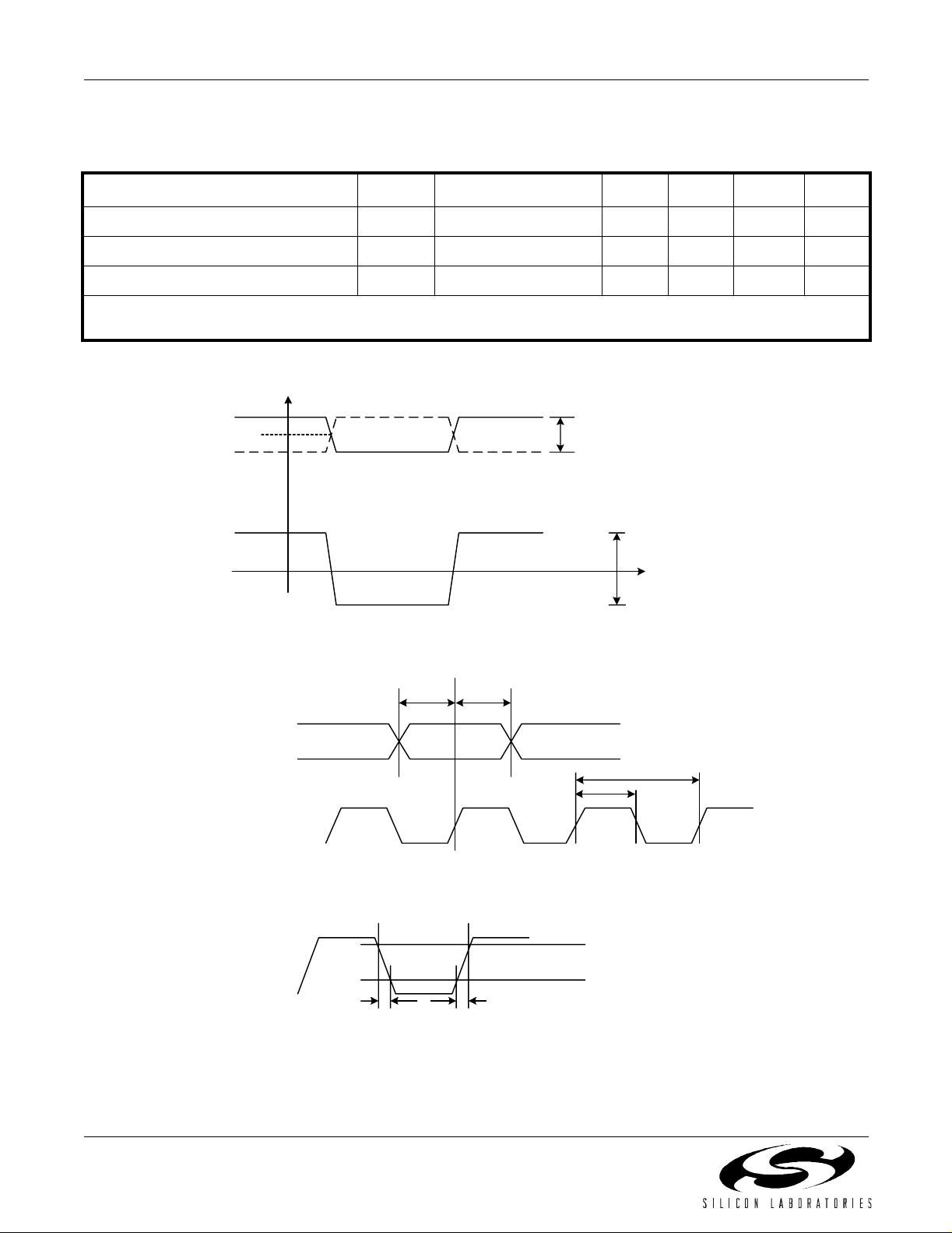
Functional Block Diagram
REFSEL
REFC LK
TXLOL
BWSEL
TXCLKD SBL
TXCLKOUT
TXDOUT
Preliminary Rev. 0.31 8/ 01 Copyright © 2001 by Silicon Labora tories Si5540-DS031
This in formation applies to a product under devel opment. I ts characteristics and specifications are subject to change without notice.
2
TXCLK16IN
2
2
Bias
REXT
DSPLL
CMU
Reset
Control
RESET
TM
TXSQLCH
TXMSBSEL
÷
16:1
16
MUX
FIFOERR
REFRATE
2
32
FIFO
2
TXCLK16OUT
TXCLK16IN
TXDIN[15:0]
FIFORST
Page 2

Si5540
2 Preliminary Rev. 0.31
Page 3

Si5540
TABLE OF CONTENTS
Section Page
Electrical Specifications . . . . . . . . . . . . . . . . . . . . . . . . . . . . . . . . . . . . . . . . . . . . . . . . . 4
Functional Description . . . . . . . . . . . . . . . . . . . . . . . . . . . . . . . . . . . . . . . . . . . . . . . . . . 9
DSPLL™ Clock Multiplier Unit . . . . . . . . . . . . . . . . . . . . . . . . . . . . . . . . . . . . . . . . . . 9
Reference Clock . . . . . . . . . . . . . . . . . . . . . . . . . . . . . . . . . . . . . . . . . . . . . . . . . . . . . 9
Serialization . . . . . . . . . . . . . . . . . . . . . . . . . . . . . . . . . . . . . . . . . . . . . . . . . . . . . . . . 9
Reset . . . . . . . . . . . . . . . . . . . . . . . . . . . . . . . . . . . . . . . . . . . . . . . . . . . . . . . . . . . . . 10
Clock Disable . . . . . . . . . . . . . . . . . . . . . . . . . . . . . . . . . . . . . . . . . . . . . . . . . . . . . . . 10
Bias Generation Circuitry . . . . . . . . . . . . . . . . . . . . . . . . . . . . . . . . . . . . . . . . . . . . . . 10
Differential Output Circuitry . . . . . . . . . . . . . . . . . . . . . . . . . . . . . . . . . . . . . . . . . . . . 11
Si5540 Pinout: 99-Pin BGA . . . . . . . . . . . . . . . . . . . . . . . . . . . . . . . . . . . . . . . . . . . . . . . 12
Pin Descriptions: Si5540 . . . . . . . . . . . . . . . . . . . . . . . . . . . . . . . . . . . . . . . . . . . . . . . . . 14
Ordering Guide . . . . . . . . . . . . . . . . . . . . . . . . . . . . . . . . . . . . . . . . . . . . . . . . . . . . . . . . . 17
Package Outline . . . . . . . . . . . . . . . . . . . . . . . . . . . . . . . . . . . . . . . . . . . . . . . . . . . . . . . . 18
Contact Information . . . . . . . . . . . . . . . . . . . . . . . . . . . . . . . . . . . . . . . . . . . . . . . . . . . . . 20
Preliminary Rev. 0.31 3
Page 4
Si5540
Electrical Specifications
Table 1. Recommended Operating Conditions
Parameter Symbol Test Condition Min* Typ
Ambient Tem peratur e T
LVTTL Output Supply Voltage V
Si5540 Supply Voltage V
*Note: All minimum and maximum speci ficat i ons are guaranteed and apply across the recommended operating condi tions.
T ypi cal val ues appl y at nominal supply voltages and an operat in g temperature of 25
A
DD33
DD
–40 25 85 °C
1.71 — 3.47 V
1.71 1.8 1.89 V
°C unless otherwise stated.
Max*
Unit
V
SIGNAL +
Differential
I/Os
V
ICM
SIGNAL –
, V
OCM
V
IS
Single Ended Voltage
(SIGNAL +) – (SIGNAL –)
Differential
Voltage Swing
VID,VOD (V
= 2VIS)
ID
Differential Peak-to-Peak Voltage
t
Figure 1. Differential Voltage Measurement (TXDIN, TXDOUT, TXCLK16IN, TXCLK16OUT)
TXDOUT,
TXDIN
TXCLKOUT,
TXCLK16IN
All Differential
IOs
t
su
t
hd
Figure 2. Data to Clock Delay
80%
20%
t
F
t
R
Figure 3. Rise/Fall Time Measurement
t
t
CH
CP
4 Preliminary Rev. 0.31
Page 5
Si5540
Table 2. DC Characteristics, VDD = 1.8 V
(VDD = 1.8 V ±5%, TA = –40°C to 85°C)
Parameter Symbol Test Condition Min Typ Max Unit
Supply Current I
Power Dissipation P
Common Mode Output Voltage
V
(TXDOUT,TXCLKOUT)
Differential Output Voltage Swing
V
(TXDOUT, TX CLKOUT), Differential pk-pk
L VPECL Input Voltage High (REFCLK) V
L VPECL Input Voltage Low (REFCLK) V
L VPECL Input Voltage Swing (REFCLK),
V
Differential pk-pk
LVPECL Input Common Mode (REFCLK) V
Input Impedance
R
(REFCLK, TXDIN, TXCLK16IN)
L VDS Input High Voltage (TXDIN,
V
TXCLK16IN)
L VDS Input Low Voltage (TXDIN,
TXCLK16IN)
LVDS Input Voltage, Single Ended pk-pk
V
(TXDIN, TXCLK 1 6 IN)
DD
D
OCM
OD
IH
IL
ID
ICM
IN
IH
V
IL
ISE
See Figure 1 800 1000 1200 mV
Each in p ut to
common mode
— 333 TBD mA
—0.6TBDW
.8 0.9 1.0 V
(pk-pk)
1.975 2.3 2.59 V
1.32 1.6 1.99 V
250 — 2600 mV
(pk-pk)
1.65 1.95 2.30 V
42 50 58 Ω
——2.4V
0.0 — — V
100 — 600 mV
(pk-pk)
LVDS Input Common Mode Voltage
(TXDIN, TXCLK 1 6 IN)
LVDS Output High Voltage
(TXCLK16OUT)
LVDS Output Low Voltage
(TXCLK16OUT)
L VDS Output Voltage, Single Ended pk-pk
(TXCLK16OUT)
LVDS Output Common Mode Voltage
(TXCLK16OUT)
Output Short to GND
(TXCLK16OUT, TXDOUT, TXCLKOUT)
Output Short to V
DD
(TXCLK16OUT, TXDOUT, TXCLKOUT)
L VTTL Input Voltage Low
(TXCLK D S BL, FIFO R ST, TXSQLCH
,
BWSEL, REFRATE, REFSEL, TXMSBSE L,
RESET
)
V
V
V
V
V
I
I
V
ICM
OH
OL
OSE
OCM
SC–
SC+
IL2
100 Ω Load
Line-to-Line
100 Ω Load
Line-to-Line
100 Ω Load
Line-to-Line, See
Figure 1
.8 2.0 2.4 V
TBD — 1.475 V
0.925 — TBD V
250 400 550 mV
(pk-pk)
1.125 1.20 1.275 V
—25TBDmA
TBD –100 — µA
——0.8V
Preliminary Rev. 0.31 5
Page 6
Si5540
Table 2. DC Characteristics, VDD = 1.8 V (Continued)
(VDD = 1.8 V ±5%, TA = –40°C to 85°C)
Parameter Symbol Test Condition Min Typ M ax Unit
Input Voltage High
(TXCLK D S BL, FIFO R ST, TXSQLCH
,
BWSEL, REFRATE, REFSEL, TXMSBSE L,
RESET
)
Input Low Current
(TXCLK D S BL, FIFO R ST, TXSQLCH
,
BWSEL, REFRATE, REFSEL, TXMSBSE L,
RESET
)
Input Hi g h Curre n t
(TXCLK D SBL, FIFORST, TXSQL C H
,
BWSEL, REFRATE, REFSEL, TXMSBSE L,
RESET
)
Input Impedance
(TXCLK D SBL, FIFORST, TXSQL C H
,
BWSEL, REFRATE, REFSEL, TXMSBSE L,
RESET
)
LVTTL Output Voltage Low
(FIFOERR, TXLOL
)
LVTTL Output Voltage High
(FIFOERR, TXLOL
)
V
V
V
I
I
R
OH2
IH2
IL
IH
IN
OL2
2.0 — — V
——10µA
——10µA
10 — — kΩ
VDD33 = 1.8 V — — 0.4 V
VDD33 = 3.3 V — — 0.4
VDD33 = 1.8 V 1.4 — — V
VDD33 = 3.3 V 2.4 — —
6 Preliminary Rev. 0.31
Page 7

Si5540
Ta ble 3. AC Characteristics (TXCLK16OUT, TXCLK16IN, TXCLKOUT, TXDIN, TXDOUT)
(V
1.8 V ±5%, TA = –40°C to 85°C)
DD =
Parameter Symbol Test Condition Min T yp Max Unit
TXCLKOUT Frequency f
clkout
— 9.95 10.7 GHz
TXCLKOUT Duty Cycle tch/tcp, Figure 2 45 — 55 %
Output Rise Time
t
R
Figure 3 — 25 — ps
(TXCLKOUT, TXDOUT)
Output Fall Time
t
F
Figure 3 — 25 — ps
(TXCLKOUT, TXDOUT)
TXCLKOUT Setup to TXDOUT t
TXCLKOUT Hold From TXDOUT t
su
hd
Output Return Loss 400 kHz–10 GHz
TXCLK16OUT Frequency f
CLKIN
Figure 2 25 — — ps
Figure 2 25 — — ps
10 GHz–16 GHz
TBD
TBD
—
—
—
—
Figure 2 — 622 667 MHz
dB
dB
TXCLK16OUT Duty Cycle tch/tcp, Figure 2 40 — 60 %
TXCLK16OUT Rise & Fall Times t
TXDIN Setup to TXCLK16IN t
TXDIN Hold from TXCLK16IN t
TXCLK16IN Frequency f
, t
R
DSIN
DHIN
CLKIN
F
100 — 300 ps
— — 300 ps
— — 300 ps
— 622 667 MHz
TXCLK16IN Duty Cycle tch/tcp, Figure 2 40 — 60 %
TXCLK16IN Rise & Fall Times t
, t
R
F
100 — 300 ps
Table 4. AC Characteristics (Clock Multiplier Characteristics)
(VDD = 1.8 V ±5%, TA = –40°C to 85°C)
Parameter Symbol Test Condition Min Typ Max Unit
Jitter Generation—Deter m inis t ic J
Jitter Generation—Ran dom J
Jitter Transfer Bandwidth J
DET(PP)
GEN(RMS)
BW
Jitter Transfer Peaking — 0.05 0.1 dB
Acquisition Time T
Input Reference Clock Frequency RC
Input Reference Clock Duty
RC
AQ
FREQ
DUTY
Cycle
Input Reference Clock Frequency
RC
TOL
Tolerance
Note: Bellcore specifications: GR-1377-CORE, Issue 5, December 1998.
PRBS-23 — 0.020 TBD UI
—0.005TBDUI
BWSEL = 0 — — 12 kHz
BWSEL = 1 — — 50 kHz
Valid REFCLK — 15 20 ms
REFRATE = 1 — 622 667 MHz
REFRATE = 0 — 155 167 MHz
40 — 60 %
–100 — 100 ppm
PP
RMS
Preliminary Rev. 0.31 7
Page 8

Si5540
Table 5. Ab so l u te M aximu m R atings
Parameter Symbol Value Unit
DC Supply Voltage V
LVTTL Input Voltage V
Differential Input Voltages V
DD
DD33
DIF
–0.5 to 3.0 V
–0.5 to 3.6 V
–0.3 to (VDD+ 0.3) V
Maximum Current any output PIN ±50 mA
Operating Junctio n Temperature T
Storage Temperature Rang e T
Package Temperature
JCT
STG
–55 to 150 °C
–55 to 150 °C
275 °C
(soldering 10 seconds )
ESD HBM To ler anc e (100 pf, 1.5 k
Note: Permanent device damage m ay occur if the above Absolute Maximum Rat ing s are exc eeded. Functional operation
should be restricted to the conditions as specified in the operational sect i ons of this dat a sheet. Exposure to absolute
maximum rating conditi ons f or ext ended periods may affec t device r eliability.
Ω)TBDV
Table 6. Thermal Ch ar acteristics
Parameter Symbol Test Condition Value Unit
Thermal Resistance Junction to Ambient ϕ
JA
Still Air 35 °C/W
8 Preliminary Rev. 0.31
Page 9

Functional Description
Si5540
The Si5540 is a fully integrated, low power, SONET/
SDH transmitter for OC-192/STM-64 applications. It
combines a high performance clock multiplier unit
(CMU) with a 16:1 serializer that has a low-speed
interface compliant with the Optical Interface Forum
(OIF) SFI-4 standard.
The CMU uses a phase-locked loop (PLL) architecture
based on Silicon Laboratories’ proprietary DSPLL
technology. This technology is used to generate u ltralow jitter clock and data outputs that provide significant
margin to the SONET/SDH specificati ons. The DSPLL
architecture also utilizes a digitally implemented loop
filter that eliminates the need for external loop filter
components. As a result, sensitive noise coupling nodes
that typically cause degraded jitter performance in
crowded PCB environments are removed .
The DSPLL also reduces the complexity and
performance requirements of reference clock
distribution strategies for OC-192/STM-64 optical port
cards. This is possible because the DSPLL provides
selectable wideband and narrowband loop filter settings
that allow the user to set the jitter attenuation
characteristics of the CMU t o accommodate reference
clock sources that have a high jitter content. Unlike
traditional analog PLL implementations, the loop filter
bandwidth is controlled by a digital filter inside the
DSPLL and can be changed without any modification to
external components.
™
DSPLL™ Clock Multiplier Unit
The Si5540’s clock multiplier unit (CMU) uses Silicon
Laboratories’ proprietary DSPLL technology to generate
a low jitter, high frequency clock source capable of
producing a high speed serial clock and data output with
significant margin to the SONET/SDH specifications.
This is achieved by using a digital signal processing
(DSP) algorithm to replace the loop filter commonly
found in analog PLL design s. This algorithm processes
the phase detector error term and generates a digital
control value to adjust the frequency of the voltage
controlled oscillat or (VCO). B ecause external loop filter
components are not required, sensitive noise entry
points are eliminated, thus making the DSPLL less
susceptible to board-level noise sources. Therefore,
SONET/SDH jitter compliance is easier to attain in the
application.
Programm able Loop Filt er B andwidth
The digital loop filter in the Si5530 provides two
bandwidth settings that support either wideband or
narrowband jitter transfer characteristics. The filter
bandwidth is selected via t he BWSEL control input. In
traditional P LL implementation s, changing the loop filter
bandwidth would require changing the values of
external loop filter co mpo nents.
In narrowband mode, a loop filter cutoff of 12 kHz is
provided. This set ting makes the Si5540 more tolerant
of jitter on th e reference clock source. As a re sult, the
complexity of the clock distribution circuitry used to
generate the physical layer reference clocks can be
simplified without compromising jitter margin to the
SONET/SDH specific ati on.
In wideband mode, the loop filter provides a cutoff of
50 kHz. This setting i s desirable in applications where
the reference clock is provided by a low jitter source like
the Si5364 Clock Synchronization IC or Si5320
Precision Clock Multiplier/Jitter Attenuator IC. This
allows the DSPLL to more closely track the precision
reference source resulting in the best possible jitter
performance.
Reference Clock
The CMU within the Si5530 i s designed to operat e with
reference c lock sourc es that ar e eith er 1/16t h or 1/64th
the desired output data rate. The CMU will support
operation with data rates between 9.9 Gbps and
10.7 Gbps and the reference clock should be scaled
accordingly. For example, to support 10.66 Gbps
operation the reference clock source would be
approximately 167 MHz or 666 MHz. The REFRATE
input pin is used to configure the device for operation
with one of the two supported reference clock
submultiples of the data rate.
The Si5540 supports operation with two selectable
reference c lock s our ces . The first configuration uses an
externally provided reference clock that is input via
REFCLK. The second configuration uses the parallel
data clock, TXCLK16IN, as the reference clock source.
When using TXCLK16IN as the reference source, the
narrowband loop filter setting may be preferable to
remove jitter that may be present on the data clock. The
selection of reference clock configuration is controlled
via the REFSEL input. The Si5540 will drive the TXLOL
output high to indicate the DSPLL has locked to the
selected reference sou rce.
Serialization
The Si5540 includes serialization circuitry that
combines a FIFO wit h a parallel to serial shift register.
Low speed data on the parallel input bus, T XDIN[15:0],
is latched into the FIFO on the rising edge of
TXCLK16IN. The data in the FIFO is clocked into the
Preliminary Rev. 0.31 9
Page 10

Si5540
shift register by an output clock, TXCLK16 OUT, that is
produced by dividing down the high speed transmit
clock, TXCLKOUT , by a factor of 16. The TXCLK16OUT
clock output is provided to su ppor t 16 bit word trans fe rs
between the Si5540 and upstream devices using a
counter clocking scheme. The high-speed serial data
stream is clocked out of the shift register using
TXCLKOUT.
Input FIFO
The Si5540 integrates a FIFO to decouple data
transferred into the FIFO via TXCLK16IN from data
transferred into th e s hift r egister via TXCLK16O UT. The
FIFO is eight parallel words deep and accommodates
any static phase delay tha t may be i ntroduc ed between
TXCLK16OUT and TXCLK16IN in counter clocking
schemes. Further, the FIFO will accommodat e a phase
drift or wander between TXCLK16IN and TXCLK16OUT
of up to three parallel data words.
The FIFO circuitry indicates an overflow or underflow
condition by ass erting FIFOERR high. This ou tput can
be used to recenter the FIFO read/write pointers by
tieing it directly to the FIFORST input. The Si5540 w ill
also recenter the read/ write pointers after the device’s
power on reset, external reset via RESET
time the DSPLL transitions from an out of lock state to a
locked state (TXLOL
Parallel Input To Serial Output Relationship
The Si5540 provides the c apability to select the order in
which data on the par allel input b us is transmi tted serially. Data on this bus can be transmitted MSB first or
LSB first depending on the setting of TXMSBSEL. If
TXMSBSEL is tied low, TXDIN0 is transmitted first followed in order by TXDIN1 through TXDIN15. If TXMSBSEL is tied high, TXDIN15 is transmitted first followed in
order by TXDIN14 th ro ugh TXDIN0. This feat ur e s im plifies board rout ing when I Cs are mounte d on bot h sides
of the PCB.
Transmit Data Squelch
To prev ent the transmission of corrupted data into the
network, the Si5540 provides a control pin that can be
used to force the high speed data output, TXDOUT, to 0.
By driving TXSQLCH
transitions from low to high).
low TXDOUT will be forced to 0.
, and each
Clock Disable
The Si5540 provides a clock disable pin, T XCLKDSBL,
that is used to disable the high -speed serial data clock
output, TXCLKOUT. When the TXCLKDSBL pin is
asserted, the positive and negative terminals of CLKOUT are tied to 1.5 V through 50
This feature is used to reduce power consumption in
applications that do not use the high speed transmit
data clock.
Ω on-chip resistors.
Bias Generation Circuitry
The Si5540 makes use of an external resistor to set
internal bias currents. The external resistor allows pr ecise generation of bias currents which significantly
reduces power consumption versus traditional implementations that use an internal resistor. The bias generation circuitry requires a 3.09 k
connected between REXT and GND.
Ω (1%) resistor
Reset
A device reset can be forced by holding the RESET pin
low for at least 1
input FIFO point er s r ese t a nd t he digital control c ir c uit ry
initializes. When RESET transitions high to start normal
operation, the DSPLL will be calibrat ed.
10 Preliminary Rev. 0.31
µs. When RESET is as serted low, the
Page 11

Si5540
Differential Output Circuitry
The Si5540 utilizes a current-mode logic (CML) architecture to drive the high speed serial output clock and data on
TXCLKOUT and TXDOUT. An example of output term ination with ac coupling is shown in Figure 4. In applic ati ons
where direct dc coup ling is possi ble, t he 250 nF capacitor s may be om itted. The differ ential peak-to -peak volta ge
swing of the CML architecture is list ed in Table 2 on page 5.
50 Ω
1.5 V
50 Ω
24 mA
250 nF
250 nF
Zo = 50 Ω
Zo = 50 Ω
VDD
50 Ω
50 Ω
VDD
Figure 4. CML Output Driver Termination (TXCLKOUT, TXDOUT)
Preliminary Rev. 0.31 11
Page 12

Si5540
Si5540 Pinout: 99 BGA
10 123456789
TXDIN[12]– TXDIN[12]+ TXDIN[14]– TXDIN[14]+ REFCLK– REFCLK+ TXSQLCH
TXDIN[10]+ TXDIN[11]+ TXDIN[13]– TXDIN[13]+ TXDIN[15]– TXDIN[15]+ TXCLKDSBL REFSEL
TXDIN[10]– TXDIN[11]– GND GND GND GND RESET VDD33 GND TXCLKOUT+
TXDIN[8]+ TXDIN[9]+ GND VDD VDD VDD VDD
TXDIN[8]– TXDIN[9]– GND VDD VDD VDD VDD
TXDIN[6]+
TXDIN[6]–
TXDIN[7]+
TXDIN[7]–
GND VDD VDD VDD VDD
GND VDD VDD VDD VDD
RSVD_
VDD33
RSVD_
GND
RSVD_
GND
RSVD_
GND
RSVD_
GND
REFRATE
RSVD_
VDD33
GND TXCLKOUT–
GND GND
GND TXDOUT+
GND TXDOUT–
GND
A
B
C
D
E
F
G
TXDIN[4]+ TXDIN[5]+ GND GND GND GND GND BWSEL NC GND
TXDIN[4]–
TXDIN[2]+
TXDIN[5]–
TXDIN[2]–
TXDIN[3]+ TXDIN[3]– TXDIN[1]+ TXDIN[1]– TXMSBSEL
TXDIN[0]+ TXDIN[0]–
TXCLK16
IN+
TXCLK16
IN–
Bottom View
Figure 5. Si5540 Pin Configuration (Bottom View)
12 Preliminary Rev. 0.31
TXCLK16
OUT+
RSVD_
GND
TXCLK16
OUT–
TXLOL REXT
FIFORST FIFOERR
H
J
K
Page 13

Si5540
10123456789
A
B
GND
REFRATE
RSVD_
VDD33
C
D
E
F
G
TXDOUT–
GNDTXCLKOUT–
GNDGND
GNDTXDOUT+
GND
RSVD_
VDD33
RSVD_
GND
RSVD_
GND
RSVD_
GND
RSVD_
GND
TXDIN[12]–TXDIN[12]+TXDIN[14]–TXDIN[14]+REFCLK-REFCLK+TXSQLCH
TXDIN[10]+TXDIN[11]+TXDIN[13]–TXDIN[13]+TXDIN[15]–TXDIN[15]+TXCLKDSBLREFSEL
GNDGNDGNDGNDRESETVDD33GNDTXCLKOUT+
GNDVDDVDDVDDVDD
VDDVDDVDD
VDDVDDVDD
VDDVDD
VDD
VDD
TXDIN[11]–
TXDIN[10]–
TXDIN[8]+TXDIN[9]+
TXDIN[8]–TXDIN[9]–GND
TXDIN[6]+TXDIN[7]+GNDVDD
TXDIN[6]–TXDIN[7]–GNDVDD
H
J
K
REXT
FIFOERR
TXLOL
FIFORST
RSVD_
GND
TXCLK16
OUT–
GNDBWSELNCGND
TXMSBSEL
TXCLK16
OUT+
TXCLK16
IN–
GNDGND
TXCLK16
IN+
TXDIN[4]+TXDIN[5]+GNDGND
TXDIN[4]–TXDIN[5]–TXDIN[3]+TXDIN[3]–TXDIN[1]+TXDIN[1]–
TXDIN[2]–TXDIN[0]+TXDIN[0]–
TXDIN[2]+
Top View
Figure 6. Si5540 Pin Configuration (Transparent Top View)
Preliminary Rev. 0.31 13
Page 14

Si5540
Pin Descr i p tio ns : Si 554 0
Pin Number(s) P in Name I/O Signal Level Description
H3 BWSEL I LVTTL
K1 FIFOERR O LVTTL
K2 FIFORST I LVTTL
B1, C5–8, C2, D8,
D2, E8, E1–2, F8,
F2, G8, G2 , H4–
8, H1
H2 NC —
A5–6 REFCLK+,
GND GND
REFCLK–
I LVPECL
Bandwidth Select DSPL L.
This input selects loop bandwidth of the DSPLL.
BWSEL = 0: Loop bandwidth set to 12 kHz
BWSEL = 1: Loop bandwidth set to 50 kHz.
FIFO Error.
This output is driven high when a FIFO overflow/underflow has occurred. This output will
stick high until reset by asserting FIFORST.
FIFO Reset.
This input, when asserted high , resets the read/
write FIFO pointers to their initial state.
GND.
No Connect.
Reserved for device testing; leav e electrically
unconnected.
Differential Reference Clock.
The reference clock sets the operating frequency of the PLL used to generate the output
clock frequency. The Si5540 will operate with
reference clock frequencies that ar e eith er 1/
16th or 1/64th the output clock rate.
A2 REFRATE I LVTTL
B3 REFSEL I LVTTL
C4 RESET
14 Preliminary Rev. 0.31
ILVTTL
Reference Frequency Select.
This input configures the CMU to operate with
one of two possible reference clock freq uencies. When REFRA TE = 1, the CMU will operate with a reference that is 1/16th the output
clock rate. When REFRATE = 0, the CMU will
operate with a reference that is 1/64th the output clock rate.
Reference Clock Selection.
This inputs selects the reference clock source
used by the CMU. When REFSEL = 0, the low
speed data input clock, TXCLK16IN, is used as
the CMU reference. When REFSEL = 1, the reference clock provided on REFCLK is used.
Device Reset.
Forcing this input low for at least 1 µs will cause
a device reset. For normal operation, this pin
should be held high.
Page 15

Pin Number(s) P in Name I/O Signal Level Description
Si5540
J1 REXT
D3, E3, F3, G3 , J3RSVD_GND —
A3, B2 RSVD_VDD33 —
K5–6 TXCLK16IN–,
TXCLK16IN+
K3–4 TXCLK16OUT+,
TXCLK16OUT–
B4 TXCLKDSBL I LVTTL
ILVDS
OLVDS
External Bias Resistor.
This resistor is used by onboard circu itry to
establish bias currents within the device. This
pin must be connected to GND through a
3.09 k
Ω (1%) resistor.
Reserved Tie to Ground.
Must tie directly to GND for proper operation.
Reserved Tie to VDD33.
Must tie directly to VDD33 for proper operat ion.
Differential Data Clock Input.
The rising edge of this input clocks data present
on TXDIN into the device.
Divided Down Output Clock.
This clock output is generated by dividing down
the high speed output clock, TXCLKOUT, by a
factor of 16. It is intended for use in counter
clocking schemes that transfer data between
the system ASIC and the Si5540.
High Speed Clock Disable.
When this input is high, the outpu t driv er for
TXCLKOUT is disabled. In applications that do
not require the output data clock, the output
clock driver should be disabled to save power.
C1, D1 TXCLKOUT+,
TXCLKOUT–
A7–10, B5–10,
C9–10, D9–10,
E9–10, F9–10,
G9–10, H9–10,
J5–10, K7–10
F1, G1 TXDOUT+,
J2 TXLOL
TXDIN[15:0]–,
TXDIN[15:0]+
TXDOUT–
OCML
ILVDS
OCML
OLVTTL
High Speed Clock Output.
The high speed output clock, TXCLKOUT , is
generated by the PLL in the clock multip lier
unit. It’s frequency is nominally 16 or 64 times
the selected reference source.
Differential Parallel Data Input.
The 16-bit data word present on these pins is
multiplexed into a high speed serial stream and
output on TXDOUT . The data on these inputs is
clocked into the device by the rising edge of
TXCLKIN.
Differential High Speed D ata Output.
The 16-bit word input on TXDIN[15:0] is multi plexed into a high speed serial stream that is
output on these pins. This output is updated by
the rising edge of TXCLKOUT.
CMU Loss-of-Lock.
The output is asserted low when the CMU is not
phase locked to the selected referenc e s our ce.
Preliminary Rev. 0.31 15
Page 16

Si5540
Pin Number(s) P in Name I/O Signal Level Description
J4 TXMSBSEL I LVTTL
A4 TXSQLCH
D4–7, E4–7,
F4–7, G4–7,
C3 VD D33 VDD33 1.8 V or 3.3 V
VDD VDD 1.8 V
ILVTTL
Data Bus Transmit Order.
For TXMSBSEL = 0, data on TXDIN[0] is transmitted first followed by TXDIN[1] through
TXDIN[15].
For TXMSBSEL = 1, TXDIN[15] is transmit ted
first followed by TXDIN[14] through TXDIN[0].
Transmit Data Squelch.
If TXSQLCH is asserted low, the output data
stream on TXDOUT will be forced to 0. If
TXSQLCH
Supply Voltage.
Nominally 1.8 V.
Digita l Out put Suppl y.
Must be tied to either 1.8 V or 3.3 V. When tied
to 3.3 V, LVTTL compa ti ble output vol tag e
swings on TXLOL
ported.
= 1, TX squelching is turned off.
and FIFOERR are sup-
16 Preliminary Rev. 0.31
Page 17

Ordering Guide
Si5540
Table 7. Ordering Guide
Part Number Package Temperature
Si5540-BC 99 B GA –40°C to 85°C
Preliminary Rev. 0.31 17
Page 18

Si5540
Package Ou tlin e
Figure 7 illustrates t he package details for the S i5540. Table 8 lists the values for the dimens ions shown in the
illustration.
A1 Ball Pad
Corner
A1 Ball Pad
Corner
D
A
A1
E
b
A2
Seating
Plane
10987654321
e
1.00 Ref
1.00 Ref
A
B
C
D
E
F
G
H
J
K
e
Bottom ViewTop View Side View
Figure 7. 99-Ball Grid Array (BGA)
Table 8. Package Diagram Di mensions
Symbol Millimeters
Min Nom Max
A 1.30 1.40 1.50
A1 0.31 0.36 0.41
A2 0.65 0.70 0.75
b — 0.46 —
D—11.00—
E—11.00—
e — 1.00 —
18 Preliminary Rev. 0.31
Page 19

NOTES:
Si5540
Preliminary Rev. 0.31 19
Page 20

Si5540
Contact Informati on
Silicon Laboratori es Inc.
4635 Boston Lane
Austin, TX 78735
Tel: 1+(512) 416-8500
Fax: 1+(512) 416-9669
Toll Free: 1+(877) 444-3032
Email: productinfo @ silabs.com
Internet : w ww.silabs .com
The information in this document is believed to be accurate in all respects at the time of publication but is subject to change without noti c e.
Silico n Laborator ies assumes no responsibilit y fo r errors and omissio ns, and disc laims responsibilit y for any consequences resulting from
the use of in form ation inclu ded her ein. Addit ionall y, Si licon Labor atories assu mes no re sponsib ility for the fu nction ing of undes cribed fea tures
or parameters. Silicon Laboratories reserves the right to make changes without further notice. Silicon Laboratories makes no warranty, rep resent ation or gu ara ntee rega rding the suit abilit y of its pro duct s for any particul ar purp ose, nor does Silicon Lab orat ories as sume an y liabili ty
arisin g out of the ap plic at ion or use of any prod uct or circ uit , and sp eci fic ally dis clai ms an y and al l liab i lity , incl udi ng without lim it ation co nsequential or incidental damages. Silicon Laboratories products are not designed, intended, or authorized for use in applications intended to
support or sustain life , or for any other applica ti on in which the failure of the Sil icon Laboratories produ ct could create a situation where personal inj ury or death may occur . Should Buyer purchase or use Silicon Laboratories prod ucts for any such unintended or unauthorized application, Buyer shall indemnify and hold Silicon Laboratories harmless against all claims and damages.
Silico n Laborator ies, Silicon Labs , SiPHY, and DSPLL are trademarks of Sili con Labor atories In c.
Other products or brandnames mentioned herein are trademarks or registered trademarks of their respective holders.
20 Preliminary Rev. 0.31
 Loading...