

Page 1
Preliminary Rev. 0.31 8/ 01 Copyright © 2001 by Silicon Labora tor ies Si5530-DS031
This information applies to a product under development. Its char acteristics and spe c ifications are subject to change without notice.
Si5530
SiPHY™ OC-192/STM-64 SONET/SDH RECEIVER
Features
Complete low power, high speed, receiver with integrated limiting amplifier,
clock and data recovery (CDR), and 1:16 demultiplexer:
Applications
Description
The Si5530 is a fully integrated low-power receiver for high-speed serial
communication systems. It combines post amplification, clock and data
recovery, and a 1:16 deserialization as required in OC-192/STM-64
applications. Support for data streams up to 10.7 Gbps is also provided for
applications that employ forward error correction (FEC). A fully integrated
clock and data recovery unit with integrated loop filter ensures optimal jitter
performance while reducing design complexity.
The Si5530 represents a new standard in low power and small size for
high-speed serial receivers. It operates from a single 1.8 V supply over the
industrial temperature range (–40°C to 85°C).
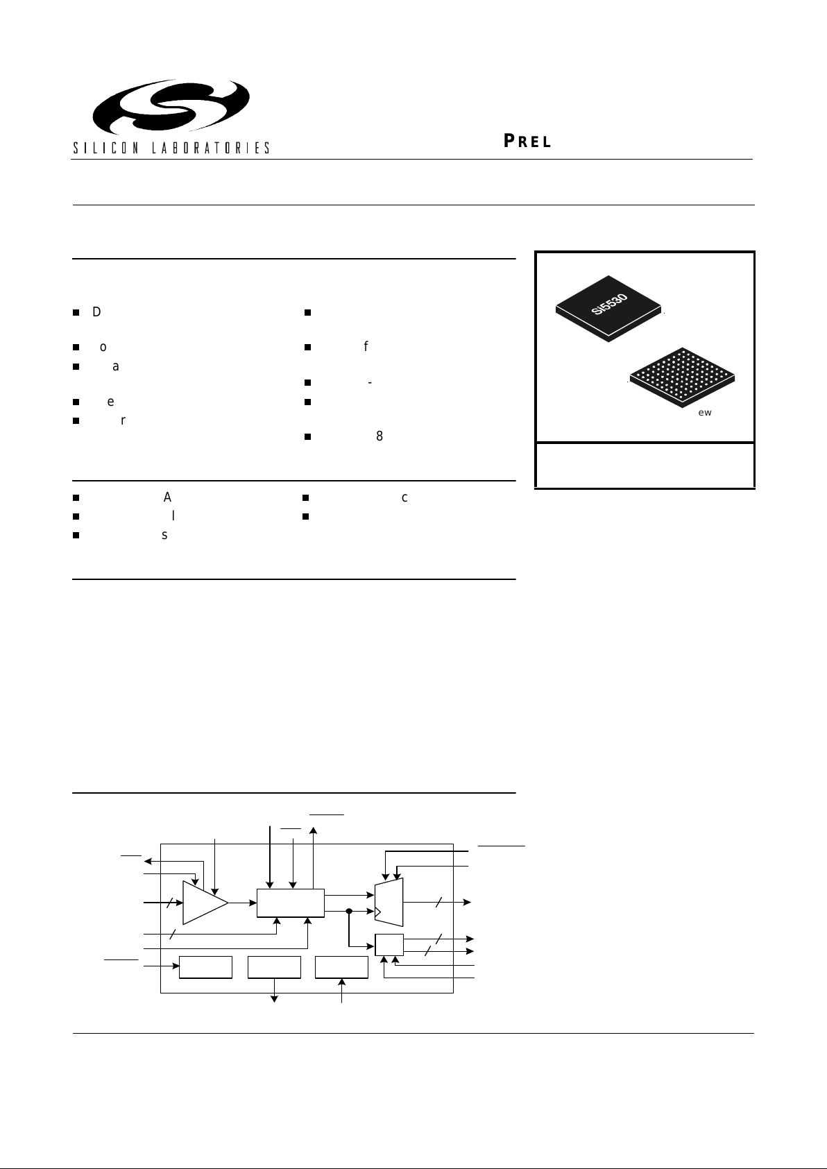
Functional Block Diagram
Data Rates Supported: OC-192/
STM-64, 10GbE, 10.7 Gbps FEC
Low Power Operation 0.6 W (typ)
Small Footprint 99-Pin BGA
Package (11 x 11 mm)
Integrated Limiting Amplifier
Programmable Slicing Level and
Sampling Phase
SFI-4 Compliant LVDS Low
Speed Interface
Loss-of-Signal and Loss-of-Lock
Detection
Lock-to-Reference Control
Optional 3.3 V Supply Pin for
LVTTL Compatible Outputs
Single 1.8 V Supply Operation
Sonet/SDH/ATM Routers
Add/Drop Multiplexers
Digital Cross Connects
Optical Transceiver Modules
Sonet/SDH Test Equipment
RXDOUT[15:0]
RXCLK1
RXCLK2
RXCLK2DIV
1:16
DEMUX
RXSQLCH
RXMSBSE L
32
2
2
RXCLK2DSBL
RXDIN
REFCLK
Limiting
AMP
LOSLVL
LOS
LTR
CDR
2
2
SLICE_LVL
PHASE_ADJ RXLOL
REFRATE
RESET
Reset
Control
Voltage
Ref
VREF
Bias
REXT
÷
Ordering Information:
See pa ge16.
Si5364
Bottom View
PRELIMINARY DATA SHEET
Page 2

Si5530
2 Preliminary Rev. 0.31
Page 3

Si5530
Preliminary Rev. 0.31 3
TABLE OF CONTENTS
Section Page
Electrical Specifications . . . . . . . . . . . . . . . . . . . . . . . . . . . . . . . . . . . . . . . . . . . . . . . . . 4
Functional Description . . . . . . . . . . . . . . . . . . . . . . . . . . . . . . . . . . . . . . . . . . . . . . . . . . 8
Limiting Amplifier . . . . . . . . . . . . . . . . . . . . . . . . . . . . . . . . . . . . . . . . . . . . . . . . . . . . 8
Loss-of-Signal Detection . . . . . . . . . . . . . . . . . . . . . . . . . . . . . . . . . . . . . . . . . . . . . . 8
Slicing Level Adjustment . . . . . . . . . . . . . . . . . . . . . . . . . . . . . . . . . . . . . . . . . . . . . . 8
Clock and Data Recovery (CDR) . . . . . . . . . . . . . . . . . . . . . . . . . . . . . . . . . . . . . . . . . . . 8
Sample Phase Adjustment . . . . . . . . . . . . . . . . . . . . . . . . . . . . . . . . . . . . . . . . . . . . . 8
Lock Detect . . . . . . . . . . . . . . . . . . . . . . . . . . . . . . . . . . . . . . . . . . . . . . . . . . . . . . . . 9
Lock-to-Reference . . . . . . . . . . . . . . . . . . . . . . . . . . . . . . . . . . . . . . . . . . . . . . . . . . . 9
Reference Clock . . . . . . . . . . . . . . . . . . . . . . . . . . . . . . . . . . . . . . . . . . . . . . . . . . . . . . . . 9
Deserialization . . . . . . . . . . . . . . . . . . . . . . . . . . . . . . . . . . . . . . . . . . . . . . . . . . . . . . . . . 9
Serial Input to Parallel Output Relationship . . . . . . . . . . . . . . . . . . . . . . . . . . . . . . . . 9
Auxiliary Clock Output . . . . . . . . . . . . . . . . . . . . . . . . . . . . . . . . . . . . . . . . . . . . . . . . . . . 9
Data Squelch . . . . . . . . . . . . . . . . . . . . . . . . . . . . . . . . . . . . . . . . . . . . . . . . . . . . . . . . . . . 9
Bias Generation Circuitry . . . . . . . . . . . . . . . . . . . . . . . . . . . . . . . . . . . . . . . . . . . . . . . . 10
Voltage Reference Output . . . . . . . . . . . . . . . . . . . . . . . . . . . . . . . . . . . . . . . . . . . . . . . . 10
Si5530 Pinout: 99-Pin BGA . . . . . . . . . . . . . . . . . . . . . . . . . . . . . . . . . . . . . . . . . . . . . . . 11
Pin Descriptions: Si5530 . . . . . . . . . . . . . . . . . . . . . . . . . . . . . . . . . . . . . . . . . . . . . . . . . 13
Ordering Guide . . . . . . . . . . . . . . . . . . . . . . . . . . . . . . . . . . . . . . . . . . . . . . . . . . . . . . . . . 16
Package Outline . . . . . . . . . . . . . . . . . . . . . . . . . . . . . . . . . . . . . . . . . . . . . . . . . . . . . . . . 17
Contact Information . . . . . . . . . . . . . . . . . . . . . . . . . . . . . . . . . . . . . . . . . . . . . . . . . . . . . 18
Page 4
Si5530
4 Preliminary Rev. 0.31
Electrical Specifications
Figure 1. Differential Volta ge Measurement (RXDIN, RXDOUT, RXCLK1, RXCLK2)
Figure 2. Data to Clock Delay
Figure 3. Rise/Fall Time Measurement
Table 1. Recommended Operating Conditions
Parameter Symbol Test Condition
Min
*
Typ
Max
*
Unit
Ambient Temperature T
A
–40 25 85 °C
LVTTL Output Supply Voltage V
DD33
1.71 — 3.47 V
Si5530 Supply Voltage V
DD
1.71 1.8 1.89 V
*Note: All minimum and maximum specifications are guaranteed and apply across the recommended operating conditions.
T ypical values apply at nominal supply voltages and an oper ating temperature of 25°C unless otherwise stated.
V
IS
VID,VOD (V
ID
= 2VIS)
Differential
I/Os
Differential
Voltage Swing
Single Ended Voltage
Differential Peak-to-Peak Voltage
SIGNAL +
SIGNAL –
(SIGNAL +) – (SIGNAL –)
V
ICM
, V
OCM
V
t
RXDOUT
RXCLK1
t
CP
t
CH
t
cq1
t
cq2
All Differential
IOs
t
F
t
R
80%
20%
Page 5
Si5530
Preliminary Rev. 0.31 5
Table 2. D C Characteri sti cs
(VDD = 1.8 V ±5%, TA = –40°C to 85°C)
Parameter Symbol Test Condition Min Typ Max Unit
Supply Current I
DD
— 278 TBD mA
Power Dissipation P
D
—0.5 TBDW
Voltage Reference (VREF) V
REF
VREF driving
10 k
Ω load
1.21 1.25 1.29 V
Common Mode Input Voltage (RXDIN) V
ICM
TBD 0.1 TBD V
Differential Input Voltage Swing (RXDIN) V
ID
See Figure 1 20 — 1.0 mV
(pk-pk)
L VPECL Input Voltage HIGH (REFCLK) V
IH
1.975 2.3 2.59 V
L VPECL Input Voltage LOW (REFCLK) V
IL
1.32 1.6 1.99 V
L VPECL Input Voltage Swing,
Differential pk-pk (REFCLK)
V
ID
Figure 1 250 — 2400 mV
(pk-pk)
L VPECL Internally Generated Input Bias
(REFCLK)
V
IB
1.65 1.95 2.3 V
L VDS Output High Voltage
(RXDOUT, RXCLK1, RXCLK2)
V
OH1
100 Ω Load
Line-to-Line
TBD — 1.475 mV
LVDS Output Low Voltage
(RXDOUT, RXCLK1, RXCLK2)
V
OL1
100 Ω Load
Line-to-Line
0.925 — TBD V
LVDS Output Voltage, Differential pk-pk
(RXDOUT, RXCLK1, RXCLK2)
V
OSE
100 Ω Load
Line-to-Line,
Figure 1
500 — 800 mV
(pk-pk)
LVDS Common Mode Voltage
(RXDOUT, RXCLK1, RXCLK2)
V
CM
1.125 — 1.275 V
Output Short to GND
(RXDOUT, RXCLK1, RXCLK2)
I
SC(–)
—25TBDmA
Output Short to V
DD
(RXDOUT, RXCLK1, RXCLK2)
I
SC(+)
TBD –100 — µA
LVTTL Input Voltage Low
(RXMSBSEL, RXCLK2DIV, RXCLK2DSBL,
RXSQLCH
, REFSE L , LTR, RESET)
V
IL2
VDD33 = 3.3 V — — 0.8 V
VDD33 = 1.8 V — — 0.7
LVTTL Input Voltage High
(RXMSBSEL, RXCLK2DIV, RXCLK2DSBL,
RXSQLCH
, REFSE L , LTR, RESET)
V
IH2
VDD33 = 3.3 V 2.0 — — V
VDD33 = 1.8 V 1.7 — —
LVTTL Input Low Current
(RXMSBSEL, RXCLK2DIV, RXCLK2DSBL,
RXSQLCH
, REFSE L , LTR, RESET)
I
IL
——10µA
LVTTL Input High Current
(RXMSBSEL, RXCLK2DIV, RXCLK2DSBL,
RXSQLCH
, REFSE L , LTR, RESET)
I
IH
——10µA
Page 6
Si5530
6 Preliminary Rev. 0.31
LVTTL Input Impedanc e
(RXMSBSEL, RXCLK2DIV, RXCLK2DSBL,
RXSQLCH
, REFSE L , LTR, RESET)
R
IN
10 — — kΩ
L VTTL Output Voltage Low
(LOS
, RXLOL)
V
OL2
VDD33 = 1.8 V — — 0.4 V
VDD33 = 3.3 V — — 0.4
L VTTL Output Voltage High
(LOS
, RXLOL)
V
OH2
VDD33 = 1.8 V 1.4 — — V
VDD33 = 3.3 V 2.4 — —
Table 3. AC Characteristics (RXDIN, RXDOUT, RXCLK1, RXCLK2)
(VDD = 1.8 V ±5%, TA = –40°C to 85°C)
Parameter Symbol T est Condition Min Typ Max Unit
Output Clock Frequency
(RXCLK1)
f
clkout
See Figure 2 — 622.08 667 MHz
Duty Cycle (RXCLK1, RXCLK2) tch/tcp, Figure 2 45 — 55 %
Output Rise and Fall Times
(RXCLK1, RXCLK2,RXD O U T)
t
R,tF
Figure 3 — 50 — ps
Data Invalid Prior to RXCLK1 t
cq1
Figure 2 — — 200 ps
Data In v a l i d After RXC L K1 t
cq2
Figure 2 — — 200 ps
Input Return Loss (RXIN) 400 kHz–10.0 GHz
10.0 GHz–16.0 GHz
18.7
TBD
—
—
—
—
dB
dB
Slicing Adjust Dynam ic Ran ge SLICELVL = 200–800 mV –20 — 20 m V
Slicing Level Offset
1
(referred to RXDIN)
SLICELVL = 200–800 mV –500 — 500
µV
Slicing Level Accuracy VSLICE –5 — 5 %
Sampling Phase Adjustment
2
PHASEADJ = 200–800 mV -45
o
—45
o
LOS Threshold Dynamic Range LOSLVL = 200–800 mV 10 — 50 mV
pk-pk
LOS Threshold Offset
3
(referred to RXDIN)
LOSLVL = 200–800 mV –500 — 500
µV
LOS Threshold Accuracy VLOS –5 — 5 %
Note:
1. Slice level (referred to RXDIN) is calculated as follows: VSLICE = (SLICE_LVL – 0.4
VREF)/15.
2. Sample Phase Offset is calcul ated as follows: PHASE OFFSET = 45° (PHASEADJ – 0.4
VREF)/0.3
3. LOS Threshold voltage (r eferred to RXDIN) is calculated as follows: VLOS = 30mV + (LOS_LVL – 0.4
VREF)/15.
Table 2. DC Characteristics (Continued)
(VDD = 1.8 V ±5%, TA = –40°C to 85°C)
Parameter Symbol Test Condition Min Typ Max Unit
Page 7

Si5530
Preliminary Rev. 0.31 7
Table 4. A C Characteri sti cs (PLL Cha r acteristics)
(VDD = 1.8 V ± 5%, TA = –40°C to 85°C)
Parameter Symbol T est Condition Min Typ Max Unit
Jitter Tolerance J
TOL(PP)
f = 2.4 kHz 15 30 — UI
PP
f = 24 kHz 1.5 3.0 — UI
PP
f = 400 kHz 1.5 3.0 — UI
PP
f = 4 MHz 0.15 0.3 — UI
PP
Acquisition Time T
AQ
——20 µs
Input Reference Clock Frequency RC
FREQ
REFRATE= 1 — 622 667 MHz
REFRATE= 0 — 155 167 MHz
Reference Clock Duty Cycle RC
DUTY
40 50 60 %
Reference Clock Frequency
Tolerance
RC
TOL
–100 — 100 ppm
Frequency Difference at which
Receive PLL goes out of Lock
(REFCLK compared to the
divided down VCO clock)
LOL TBD 600 1000 ppm
Frequency Difference at which
Receive PLL goes into Lock
(REFCLK compared to the
divided down VCO clock)
LOCK TBD 300 TBD ppm
Note: Bellcore specifications: GR-1377-CORE, Issue 5, December 1998.
Table 5. A b so l u te M aximum R atings
Parameter Symbol Value Unit
DC Supply Voltage V
DD
–0.5 to TBD V
LVTTL Input Voltage V
DD33
–0.5 to 3.6 V
Differential Input Voltages V
DIF
–0.3 to (VDD+ 0.3) V
Maximum Current any output PIN ±50 mA
Operating Junction Temperature T
JCT
–55 to 150 °C
Storage Temperature Range T
STG
–55 to 150 °C
Package Temperature
(soldering 10 seconds)
275
°C
ESD HBM Tolerance (100 pf, 1.5 k
Ω)TBDV
Note: Permanent device damage m ay occur if the above Absolute Maximum Ratings are exceeded. Func ti onal operation
should be restricted to the conditions as specified in the operational sections of this data sheet. Exposure to absolute
maximum rating condit ions for extended periods may affect device re li ability.
Table 6. Thermal Ch ar acteristics
Parameter Symbol Test Condition Value Unit
Thermal Resistance Junction to Ambient ϕ
JA
Still Air 38 °C/W
Page 8

Si5530
Preliminary Rev. 0.31 8
Functional Description
The Si5530 is a high performance, low power, fully
integrated receiver for SONET/SDH applications
operating at OC-192/ST M-64 data rate s. It saves board
space by integrating a limiting amplifier, clock and data
recovery unit, and a demultiplexer into a small 99-pin
BGA package. Further space savings are realized
because no external loop filter components are required
to support CDR operation. The Si5530 also provides a
low-speed LVDS interface that is compliant to the
Optical Interface Forums SFI-4 standard.
To support long haul transmission applications,
operation at data rates up to 10.7 Gbps is support ed to
accommodate forward error correction (FEC). In
addition, programmable data slicing and sampling
phase adjustment a re provided to support bit- error-rate
(BER) optimization.
Limiting Amplifier
The Si5530 incorporates a high sensitivity limiting
amplifier with sufficient gain to directly accept the output
of transimpedance amplifiers. High sensitivity is
achieved by using a digital calibration algorithm to
cancel out amplifier offsets. This algorithm achieves
superior offset cancellation by using statistical
averaging to remove noise that can degrade more
traditional calibra tion routines.
The limiting amplifier provides sufficient gain to fully
saturate with input signals that are less than 20 mV
peak-to-peak differentia l. In addition, input signals that
exceed 1 V peak-to-peak differen tial will not cause any
performance degradation.
Loss-of-Signal Detection
The limiting am plifie r incl udes circ uitry t hat g enerates a
loss-of-signal (LOS
) alarm when the input signal
amplitude on RXDIN falls below an externally control led
threshold. The Si5530 can be configured to drive the
LOS
output low when the differential input amplitude
drops below a threshold set between ~10 mV and
50 mV pk-pk differential. Approximately 3 dB of
hysteresis prevents unnecessa ry switc hing on LOS
.
The LOS threshold is set by applying a voltage between
0.20 V and 0.80 V to the LOSLVL input. The voltage
present on LOSLVL maps to an input signal threshold
as follows:
V
LOS
is the differential pk-pk LOS threshold referred to
the RXDIN input, V
LOSLVL
is the voltage applied to the
LOSLVL pin, and VREF is reference voltage output on
the VREF pin.
The LOS detection circuitry is disabled by tieing the
LOSLVL input to the supply (VDD). T his forces the LOS
output high.
Slicing Level Adjustment
To support applications that require BER optimization,
the limiting amplifier provides circuitry that supports
adjustment of t he 0/1 decision threshold (slicing l evel)
over a range of ±20 mV when referred to the RXDIN
input. The slicing level is set by applying a voltage
between 0.20 V and 0.80 V to the SLICELVL input. The
voltage present o n SLICELV L sets the slicing level as
follows:
V
LEVEL
is the slicing l evel referred to the RXDI N input,
V
SLICE
is the voltage applied to the SLICE_LVL pin, and
VREF is reference voltage output on the VREF pin.
The slicing lev el adjustment may be disabled by tiei ng
the SLCLVL input to the supply (VDD). When slicing is
disabled, the slicing offset is set to 0.0 V relative to
internally biased input common mode voltage for
RXDIN.
Clock and Data Recovery (CDR)
The Si5530 uses an integrated CDR to recover clock
and data from a non-return to zero (NRZ) signal input on
RXDIN. The recovered data clock is used to regenerate
the incoming data by sam pling the output of the limi ting
amplifier at the center of the NRZ bit period. The
recovered clock and data is then deserial ized by a 1: 16
demultiplexer and output via a LVDS compatible low
speed interface (RXDOUT[15:0], RXCLK1, and
RXCLK2).
Sample Phase Adjustment
In applications where it is not desirable t o recover d ata
by sampling in the center of the data eye, the Si5530
supports adjustment of the CDR sampling phase across
the NRZ data period. When sample phase adjustment is
enabled, the sampling instant used for data recovery
can be moved over a range of ±45
° relative to the center
of the incoming NRZ bit period. Adjustment of the
sampling phase is de sirable when data eye distortions
are introduced by the transmission medium.
The sample phas e is s et by applying a voltage betwe en
0.20 V and 0.80 V t o the PHASEADJ input. The voltage
present on PHASEADJ maps to sam ple phase off set as
follows:
V
LOS
V
LOSLVL
0.4xVR EF–
()
15
--------------------------------------------------------------- 30 mV+=
V
LEVEL
V
SLICE
0.4xVREF–
()
15
---------------------------------------------------------- -
=
Page 9

Si5530
9 Preliminary Rev. 0.31
Phase Offset is the sa mpling off set in deg rees from the
center of the data eye, V
PHASE
is the voltage applie d to
the PHASEADJ pin, and VREF is reference voltage
output on the VREF pin. A positive phase offset will
adjust the sampli ng point to lead the de fault samp ling
point at the center of the data eye, and a negative
phase offset will adjust the sampling point to lag the
default sampling point.
Data recovery using a sampling phase offset is disabled
by tieing t he PHASEADJ input to the suppl y (VDD). Thi s
forces a default phase offset of 0
° to be used for data
recovery.
Lock Detect
The Si5530 provides lock-detect circuitr y that indicates
whether the PLL has achieved frequency lock with the
incoming data. This circuit compares the frequen cy of a
divided down version of the recovered clock with the
frequency of the s upplied reference c lock (REFCLK). If
the recovered clo ck freque ncy deviat es from that o f the
reference clock by the amount specified in Table 4 on
page 7, the PLL is declared out of lock, and the loss-oflock (RXLOL
) pin is assert ed. In this s tate, the PLL will
try to reacquire lock with the incoming data stream.
During reacquisition, the recovered clock frequency
(RXCLK1 and RXCLK2) will drift over a 1% range
relative to the supplied reference clock. The RXLOL
output will remain asserted until the recovered clock
frequency is within the REFCLK frequency by the
amount specified in T able 4 on page 7.
Lock-to-Reference
In applications where it is desirable to main tain a stable
output clock during an alarm condition like loss-ofsignal, the lock-t o-referen ce input (LTR
) can be used to
force a stable output clock . When LTR
is asserted, the
CDR is prevented from acquiring the data signal and the
CDR will lock the RXCLKOUT1 and RXCLKOUT2
outputs to the provided REFCLK. In typical applications,
the LOS
output would be tied to the LTR input to force a
stable output clock.
Reference Clock
The CDR within the S i5530 uses a reference clock to
center the PLL fre quency so that it is close e nough to
the data frequency to achieve lock. The device is
designed to oper ate with reference clock so urces that
are either 1/16th or 1/64th the input data rate. The
Si5530 will operate with data streams between
9.9 Gbps and 10.7 Gbps and the reference clock should
be scaled accordingly. For example, to support
10.66 Gbps operation the REFCLK frequencies would
be approximately 166 MHz or 666 MH z. The REFRATE
input pin is us ed to configure the device for op eration
with one of the two supported reference clock
submultiples of the data rate.
Deserialization
The Si5530 uses a 1:16 dem ult ipl ex er to deserialize the
high-speed input . The deserialized data is out put on a
16-bit parallel data bus RXDOUT[15:0] synchronous
with the rising edge of RXCLK1. This clock output is
derived by dividing down the recovered clock by a factor
of 16.
Serial Input to Parallel Output Relationship
The Si5530 provides the capabi lit y to se lect the order in
which the receiv ed s erial data is m apped t o the paralle l
output bus RXDOUT[15:0]. The mapping of the receive
bits to the output data word is controlled by the
RXMSBSEL input. If RXMSBSEL is tied low, the first bit
received is output on RXDOUT0 and the followi ng bits
are output in order on RXDOUT1 through RXDOUT15.
If RXMSBSEL is tied high, the first bit received is output
on RXDOUT15, and the following bits are output in
order on RXDOUT14 through RXDOUT0.
Auxiliary Clock Output
To support the widest range of system timing
configurations, a second clock output is provided on
RXCLK2. This output can be configured to provide a
clock that is a 1/1 6th or 1/64th submultiple of the high
speed recovered clock. The divide factor used to
generate RXCLK2 is controlled via the RXCLKDIV2
input as described in "Pin Descriptions: Si5530" on
page 13. In application s whic h do not us e RXC LK2 , this
output can be powered down by forcing the
RSCLK2DSBL input high.
Data Squelch
During some system error conditions, such as LOS, it
may be desirable to force the receive data output to
zero in order to avoid propagation of erroneous data
into the downstream electronics. In these applications ,
the Si5530 provides a data squelching control input,
RXSQLCH
. When this input is active low, the data on
RXDOUT will be forced to 0.
PhaseOffset
45°xV
PHASE
0.4xVREF–
()
0.30
--------------------------------------------------------------------------
=
Page 10

Si5530
Preliminary Rev. 0.31 10
Bias Generation Circuitry
The Si5530 makes use of an external resistor to set
internal bias currents. The external resistor allows
precise generation of bias currents which significantly
reduces power consumption versus traditional
implementations that us e an internal resistor. The bias
generation circuitry requires a 3.09 k
Ω (1%) resistor
connected between REXT and GND.
Vo ltage Ref er en ce Outp ut
The Si5530 provides an output voltage reference that
can be used by an external circuit to set the LOS
threshold, slicing level, or sampling pha se adjust. One
possible implementation would use a resistor divider to
set the control voltage for LOSLVL, SLICELVL, or
PHASEADJ. A second alternative would use a DAC to
set the control voltage. Using this approach, VREF
would be used to establish the range of a DAC output.
The reference voltage is nominall y 1.25 V.
Page 11

Si5530
Preliminary Rev. 0.31 11
Si5530 Pinout: 99 BGA
Figure 4. Si5530 Pin Configuration (Bottom View)
Bottom View
RXDOUT[4]+ RXDOUT[2]– RXDOUT[2]+ RXDOUT[0]– RXDOUT[0]+ RXCLK[1]– RXCLK[1]+
RXCLK2
DSBL
REXT
RXDOUT[4]– RXDOUT[3]– RXDOUT[3]+ RXDOUT[1]– RXDOUT[1]+ RXCLK[2]– RXCLK[2]+ NC VREF SLICELVL
RXDOUT[6]+ RXDOUT[5]+ GND GND GND GND GND
RSVD_
GND
LOSLVL PHASEADJ
RXDOUT[6]– RXDOUT[5]– GND VDD VDD VDD VDD RXSQLCH GND GND
RXDOUT[8]+ RXDOUT[7]+ GND VDD VDD VDD VDD
RSVD_
GND
GND RXDIN+
RXDOUT[8]– RXDOUT[7]– GND VDD VDD VDD VDD
RSVD_
GND
GND RXDIN–
RXDOUT[10]+ RXDOUT[9]+ GND VDD VDD VDD VDD
RSVD_
VDD33
GND GND
RXDOUT[10]– RXDOUT[9]– GND GND GND GND GND VDD33
RSVD_
GND
LTR
RXDOUT[12]+ RXDOUT[11]+ RXDOUT[11]– RXDOUT[13]+ RXDOUT[13]– RXDOUT[15]+ RXDOUT[15]– REFRATE
RSVD_
VDD33
RXLOL
RXDOUT[14]+ RXDOUT[14]– REFCLK+ REFCLK–
RSVD_
GND
RXMSBSEL RXCLK2DIV RESET LOS
RXDOUT[12]–
10 123456789
A
K
J
G
H
F
E
D
C
B
Page 12

Si5530
12 Preliminary Rev. 0.31
Figure 5. Si5530 Pin Configuration (Transparent Top View)
G
VDD
E
Top View
RXDOUT[4]+RXDOUT[2]–RXDOUT[2]+RXDOUT[0]–RXDOUT[0]+RXCLK[1]–RXCLK[1]+
RXCLK2
DSBL
REXT
RXDOUT[4]–RXDOUT[3]–RXDOUT[3]+RXDOUT[1]–RXDOUT[1]+RXCLK[2]–RXCLK[2]+NCVREFSLICELVL
RXDOUT[6]–
RXDOUT[8]+RXDOUT[7]+
RXDOUT[8]–RXDOUT[7]–GND
RXDOUT[10]+RXDOUT[9]+GND
RXDOUT[10]–RXDOUT[9]–GNDGNDGND
RXDOUT[12]+RXDOUT[11]+RXDOUT[11]–RXDOUT[13]+RXDOUT[13]–
RXDOUT[14]+RXDOUT[14]–REFCLK+REFCLK–
RSVD_
GND
RXMSBSELRXCLK2DIV
RXDOUT[12]–
10123456789
A
H
B
RXDOUT[15]+RXDOUT[15]–REFRATE
RSVD_
VDD33
RXLOL
J
GNDGNDVDD33
RSVD_
GND
LTR
VDDVDDVDD
RSVD_
VDD33
GNDGND
VDDVDDVDDVDD
RSVD_
GND
GNDRXDIN–
F
VDDVDDVDDVDD
RSVD_
GND
GNDRXDIN+ GND
RXDOUT[5]–GNDVDDVDDVDDVDDRXSQLCHGNDGND
D
RXDOUT[5]+GNDGNDGNDGNDGND
RSVD_
GND
LOSLVLPHASEADJ
C
RXDOUT[6]+
K
RESETLOS
Page 13

Si5530
Preliminary Rev. 0.31 13
Pin Descr ip t io ns : Si 553 0
Pin Number(s) Name I/O Signal Level Description
C4–8, D8, D1–
2, E8 , E2, F8,
F2, G8, G1–2,
H4–8
GND GND
GND.
K1 LOS OLVTTL
Loss-of-Signal.
This output is driven low when the peak-to-pea k
signal amplitude is below thres hold s et via
LOSLVL.
C2 LOSLVL I —
LOS Thresh ol d Lev el.
Applying an analog voltage to this pin allows
adjustment of the Threshold used to declare
LOS. Tieing this input high disables LOS detection and forces the LOS
output high.
H1 LTR
ILVTTL
Lock-to-Reference.
This input forces a stable output clock by locking
RXCLK1 and RXCLK2 to the provided reference. Driving LTR low activates this feature.
B3 NC
No Connect.
Reserved for device testing leave elec t r ic ally
unconnected.
C1 PHASEADJ I —
Sampling Phase Adjust.
Applying an analog voltage to this pin allows
adjustment of the sampling phase across the
data eye. Tieing this input high nominally centers
the sampling phase.
K6–7 REFCLK–,
REFCLK+
I LVPECL
Differential Reference Clock.
The reference clock sets the initial operating frequency used by the onboard PLL for clock and
data recovery. The device will operate with reference frequencies that are 1/16th or 1/64th the
input data rate (nominally 155 MHz or 622 MHz).
J3 REFRATE I LVTTL
Reference Clock Select.
This input configures the Si5530 to operate with
one of two reference clock frequencies. If REFSEL is held high, the device requires a reference
clock that is 1/16 the input data rate. If REFSEL
is low, a reference clock at 1/64 the input data
rate is required.
K2 RESET
ILVTTL
Device Reset.
Forcing this input low for a at least 1µs will cause
a device reset. For normal operation, thi s pin
should be held high.
Page 14

Si5530
14 Preliminary Rev. 0.31
A2 REXT
External Bias Resistor.
This resistor is used by onboard circuitr y to
establish bias currents within the device. This pin
must be connected to GND through a 3.09 k
Ω
(
1%) resistor.
C3, E3, F3, H2, K5RSVD_GND
Reserved Tie to Ground.
Must tie directly to GND for proper operation.
G3, J2 RSVD_VDD33
Reserved Tie to VDD33.
Must tie directly to VDD33 for proper operation.
A4–5 RXCLK1+,
RXCLK1–
OLVDS
Differential Clock Output 1.
The clock recovered from the signal present on
RXDIN is divided down by 16 and output on
CLKOUT. In the absence of data, a stable clock
on RXCLK1 can be maintained by asserting
LTR
.
B4–5 RXCLK2+,
RXCLK2–
OLVDS
Differential Clock Output 2.
An auxiliary output clock is provided on this pin
that may be a divided down version of the high
speed clock recovered from the signal pre se nt
on RXDIN. The divide factor used in generating
RXCLK2 is set via RXCLK2DIV.
K3 RXCLK2DIV I LVTTL
Clock Divider Select.
This input selects the divide factor used to generate the RXCLK2 output. When this input is
driven low, RXCLK2 is 1/16th the recovered
high-speed clock. When driven high, RXCLK2 is
1/64th the recovered high speed clock rate.
A3 RXCLK2DSBL I LVTTL
RXCLK2 Disable.
Driving this input high will disable the RXCLK2
output. This would be used to save power in
applications that do not require an aux iliary
clock.
E1, F1 RXDIN+,
RXDIN–
I High Speed
Differential
Differential Data Input.
Clock and data are recovered from the high
speed data signal present on these pins.
A6–10, B6–10,
C9–10, D9–10,
E9–10, F9–10,
G9–10, H9–10,
J4–10, K8–10
RXDOUT[15:0]–,
RXDOUT[15:0]+
OLVDS
Differential Parallel Data Output.
The data recovered from the signal present on
RXDIN is demultiplexed and output as a 16-bit
parallel word via RXDOUT[15:0]. These outputs
are updated on the rising edge of RXCLK1.
J1 RXLOL
OLVTTL
Loss-of-Lock.
This output is driven low when the recovered
clock frequency deviates from the reference
clock by the amount specified in Table 4.
Pin Number(s) Name I/O Signal Level Description
Page 15

Si5530
Preliminary Rev. 0.31 15
K4 RXMSBSEL I LVT TL
Data Bus Receive Order.
This determines the order of the received data
bits on the output bus.
For RXMSBSEL = 0, the first data bit received is
output on RXDOUT[0] and following data bits are
output on RDOUT[1] through RXDOUT[15].
For RXMSBSEL = 1, the first data bit is output
on RXDOUT[15] and following data bits are output on RXDOUT[14] through RXDOUT[0].
D3 RXSQLCH
ILVTTL
Data Squelch.
When this input is low, the data on RXDOUT is
forced to 0. Set RXSQLCH
high for normal oper-
ation.
B1 SLICELVL I —
Slicing Level Adju s t ment .
Applying an analog voltage to this pin allows
adjustment of the slicing level applied to the
input data eye. Tieing this input high nominally
sets the slicing offset to 0.
D4–7, E4–7,
F4–7, G4–7,
VDD VDD 1.8 V
Supply Voltage.
Nominally 1.8 V.
H3 VDD33 VDD33 1.8 V or 3.3 V
Digital Output Su pply.
Must be tied to either 1.8 V or 3.3 V. When tied
to 3.3 V, LVTTL compatible output voltage
swings on RXLOL
and LOS are supported.
B2 VREF O Voltage Ref
Voltage Reference.
The Si5600 provides an output voltage reference
that can be used by an external circuit to set the
LOS threshold, slicing le vel, or sa mpl ing phas e
adjustment. The equivalent resistance between
this pin and GND should not be less than 10 k
Ω.
The reference voltage is nominally 1.2 5 V.
Pin Number(s) Name I/O Signal Level Description
Page 16

Si5530
16 Preliminary Rev. 0.31
Ordering Guide
Table 7. Ordering Guide
Part Number Package Temperature
Si5530-BC 99 BGA –40°C to 85°C
Page 17

Si5530
Preliminary Rev. 0.31 17
Package Ou tlin e
Figure 6 illustrat es the package details for the Si5530. Table 8 lists the v alues for the dimensions shown in the
illustration.
Figure 6. 99-Ba l l Gr id Array (BGA)
Table 8. Package Diagram Dim en sions
Symbol Millimeters
Min Nom Max
A 1.30 1.40 1.50
A1 0.31 0.36 0.41
A2 0.65 0.70 0.75
b — 0.46 —
D—11.00—
E—11.00—
e — 1.00 —
D
E
10987654321
A
B
C
D
E
F
G
H
J
K
A
1 Ball P ad
Corner
A1 Ball Pad
Corner
Seating
Plane
A
A1
A2
e
Bottom ViewTop View Side Vie w
1.00 Ref
1.00 Ref
b
e
Page 18

Si5530
18 Preliminary Rev. 0.31
Contact Informatio n
Silicon Laboratori es Inc.
4635 Boston Lane
Austin, TX 78735
Tel: 1+(512) 416-8500
Fax: 1+(512) 416-9669
Toll Free: 1+(877) 444-3032
Email: productinfo @ silabs.com
Internet : w ww.silabs .com
Silico n Laboratories, Silicon Labs, and S iPHY are trademarks of Silicon Laboratories Inc.
Other products or brandnames mentioned herein are trademarks or registered trademarks of their respective holders.
The information in this document is believed to be accurate in all respects at the time of publication but is subject to change without notice.
Silico n Laboratori es assumes no responsibility for err ors and omissions, and disclaims responsibil it y f or any consequences resulting from
the use of in format ion inclu ded her ein. Addit ionall y, Si licon Labor atories assu mes no respo nsib ility for the func tion ing of undes cribed fea tures
or parameters. Silicon Laboratories reserves the right to make changes without further notice. Silicon Laboratories makes no warranty , represent ation or gu ara ntee rega rding the suit abilit y of its pro duct s for any particul ar purp ose, nor does Si licon Lab orat ories as sume an y liabili ty
arisin g out of the ap plic at ion or use of any prod uct or circ uit , and sp ecif ic ally dis clai ms an y and al l liab i lity , inclu di ng wi thout limitation consequential or incidental damages. Silicon Laboratories products are not designed, intended, or authorized for use in applications intended to
support or sustain life, or for any other application in which the failure of the Sil icon Labo r atories p roduct coul d create a s ituation where personal injury or death may occur. Should Buyer purcha se or use Silicon Laborat ories prod ucts for any such unintended or unauthorized application, Buyer shall indemnify and hold Silicon Laboratories harmless against all claims and damages.
 Loading...