

Page 1
RECISION CLOCK MULTIPLIER/REGENERATOR
P
Features
Complete precision clock multiplier and clock regenerator device:
Si5310
P
RELIMINARY DATA SHEET
IC
!
Performs Clock Multiplication to
One of Two Frequency Ranges:
150–167 MHz or 600–668 MHz
!
Jitter Generation as low as
0.5 ps
!
Accepts Input Clock from
for 622 MHz Output
RMS
9.4–668 MHz
!
Regenerates a “Clean”, JitterAttenuated Version of Input
Clock
!
DSPLL™ Technology Provides
Superior Jitter Performance
!
Small Footprint: 4 mm x 4 mm
!
Low Power: 310 mW typical
Applications
!
SONET/SDH Systems
!
Terabit Routers
!
Digital Cross Connects
!
Optical Transceiver Modules
!
Gigabit Ethernet Systems
!
Fibre Channel
Description
The Si5310 is a fully integrated low-power clock multiplier and clock
regenerator IC. The clock multiplier generates an output clock that is an
integer multiple of the input clock. The clock regenerator operates
simultaneously, creating a “clean” version of the input clock by using the
clock synthesis phase-locked loop (PLL) to remove unwanted jitter and
square up the input clock’s rising and falling edges. The Si5310 uses
Silicon Laboratories patented DSPLL
jitter performance while eliminating the analog loop filter found in
traditional PLL designs with a digital signal-processing algorithm.
The Si5310 represents a new standard in low jitter, small size, low power,
and ease-of-use for clock devices. It operates from a single 2.5 V supply
over the industrial temperature range (–40°C to 85°C).
™
architecture to achieve superior
Ordering Information:
See page 20.
Pin Assignments
Si5310-BM
NC
20 19 18 17 16
REXT
1
VDD
2
GND
3
REFCLK+
REFCLK–
4
5
6 7 8 9 10
LOL
M ULTSEL
GND
Pa d
VDD
MULTOUT–
MULTOUT+
GND
15
PW RD N
VDD
14
CLKOUT+
13
12
CLKOUT–
11
VDD
GND
CLKIN–
CLKIN+
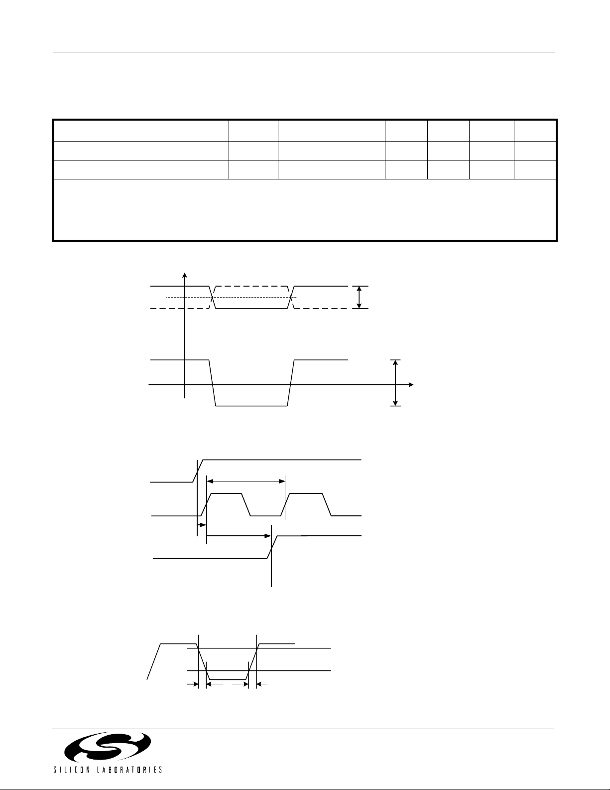
Functional Block Diagram
2
CLKIN+
CLKIN–
Regeneration
TM
2
BUF
DSPLL
Phase-Locked
Calibra tion
Loop
2
REFCLK+
REFCLK–
MULTSE L
Bias Gen
BUF
BUF
REXT
Preliminary Rev. 0.6 6/01 Copyright © 2001 by Silicon Laboratories Si5310-DS06
This information applies to a product under development. Its characteristics and specifications are subject to change without notice.
2
CLKOUT+
CLKOUT–
PWRD N/CAL
MULTOUT+
MULTOUT–
LOL
Page 2

Si5310
2 Preliminary Rev. 0.6
Page 3

Si5310
T
ABLE OF
C
ONTENTS
Section Page
Detailed Block Diagram . . . . . . . . . . . . . . . . . . . . . . . . . . . . . . . . . . . . . . . . . . . . . . . . . . 4
Electrical Specifications . . . . . . . . . . . . . . . . . . . . . . . . . . . . . . . . . . . . . . . . . . . . . . . . . 5
Functional Description . . . . . . . . . . . . . . . . . . . . . . . . . . . . . . . . . . . . . . . . . . . . . . . . . . 12
DSPLL™ . . . . . . . . . . . . . . . . . . . . . . . . . . . . . . . . . . . . . . . . . . . . . . . . . . . . . . . . . . 14
Clock Multiplier . . . . . . . . . . . . . . . . . . . . . . . . . . . . . . . . . . . . . . . . . . . . . . . . . . . . . . 14
1x Multiplication . . . . . . . . . . . . . . . . . . . . . . . . . . . . . . . . . . . . . . . . . . . . . . . . . . . . . 14
Clock Regeneration . . . . . . . . . . . . . . . . . . . . . . . . . . . . . . . . . . . . . . . . . . . . . . . . . . 14
Reference Clock . . . . . . . . . . . . . . . . . . . . . . . . . . . . . . . . . . . . . . . . . . . . . . . . . . . . . 14
DSPLL Lock Detection (Loss-of-Lock) . . . . . . . . . . . . . . . . . . . . . . . . . . . . . . . . . . . . 14
PLL Performance . . . . . . . . . . . . . . . . . . . . . . . . . . . . . . . . . . . . . . . . . . . . . . . . . . . . 15
Device Power-Down . . . . . . . . . . . . . . . . . . . . . . . . . . . . . . . . . . . . . . . . . . . . . . . . . . 15
PLL Self-Calibration . . . . . . . . . . . . . . . . . . . . . . . . . . . . . . . . . . . . . . . . . . . . . . . . . . 15
Device Grounding . . . . . . . . . . . . . . . . . . . . . . . . . . . . . . . . . . . . . . . . . . . . . . . . . . . 15
Bias Generation Circuitry . . . . . . . . . . . . . . . . . . . . . . . . . . . . . . . . . . . . . . . . . . . . . . 15
Differential Input Circuitry . . . . . . . . . . . . . . . . . . . . . . . . . . . . . . . . . . . . . . . . . . . . . . 16
Differential Output Circuitry . . . . . . . . . . . . . . . . . . . . . . . . . . . . . . . . . . . . . . . . . . . . 16
Pin Descriptions: Si5310-BM . . . . . . . . . . . . . . . . . . . . . . . . . . . . . . . . . . . . . . . . . . . . . . 18
Ordering Guide . . . . . . . . . . . . . . . . . . . . . . . . . . . . . . . . . . . . . . . . . . . . . . . . . . . . . . . . . 20
BM Package Outline . . . . . . . . . . . . . . . . . . . . . . . . . . . . . . . . . . . . . . . . . . . . . . . . . . . . . 21
Contact Information . . . . . . . . . . . . . . . . . . . . . . . . . . . . . . . . . . . . . . . . . . . . . . . . . . . . . 22
Preliminary Rev. 0.6 3
Page 4
Si5310
Detailed Block Diagram
CLKIN+
CLKIN–
REFCLK+
REFCLK+
REFCLK–
MULTSEL
REXT
Detector
Detector
Detector
Bias
Bias
Bias
Generation
Generation
Generation
Phase
Phase
Phase
A/D
DSP
n
Lock
Detector
Figure 1. Detailed Block Diagram
VCO
Calibration
CLK
Divider
Regen
Retime
Retime
c
CLKOUT+
CLKOUT–
c
MULTOUT+
MULTOUT–
LOL
PWRDN/CAL
4 Preliminary Rev. 0.6
Page 5
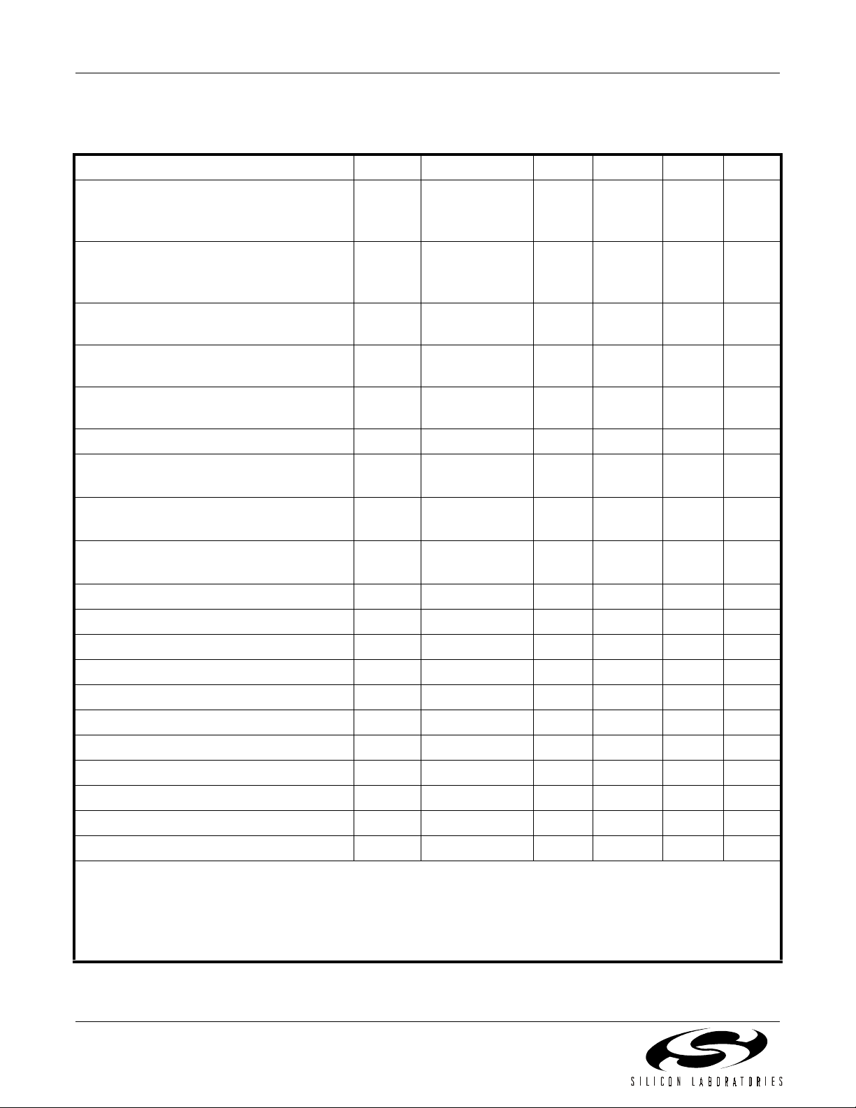
Electrical Specifications
Table 1. Recommended Operating Conditions
Si5310
Parameter Symbol Test Condition
Ambient Temperature T
Si5310 Supply Voltage
2
A
V
DD
1
Min
Typ
–40 25 85 °C
2.375 2.5 2.625 V
Max
1
Notes:
1. All minimum and maximum specifications are guaranteed and apply across the recommended operating conditions.
Typical values apply at nominal supply voltages and an operating temperature of 25°C unless otherwise stated.
2. The Si5310 specifications are guaranteed when using the recommended application circuit (including component
tolerance) of Figure 5 on page 11.
V
SIGNAL +
Differential
I/Os
V
ICM
SIGNAL –
, V
OCM
V
IS
(SIGNAL +) – (SIGNAL –)
Differential
Voltage Swing
VID,V
OD
Differential Peak-to-Peak Voltage
t
Unit
Figure 2. Differential Voltage Measurement (CLKIN, REFCLK, CLKOUT, MULTOUT)
CLKIN
MULTOUT
CLKOUT
t
CI-M
1/f
t
M-CO
MULT
Figure 3. CLKIN to CLKOUT, MULTOUT Phase Relationship
CLKIN,
REFCLK,
CLKOUT,
MULTOUT
t
F
t
R
80%
20%
Figure 4. Clock Input and Output Rise/Fall Times
Preliminary Rev. 0.6 5
Page 6
Si5310
Table 2. DC Characteristics, VDD = 2.5 V, 622 Mbps (MULTSEL = 0)
(VDD = 2.5 V ± 5%, TA = –40°C to 85°C)
Parameter Symbol Test Condition Min Typ Max Unit
Supply Current
MULTSEL = 0
MULTSEL = 1
Power Dissipation
MULTSEL = 0
MULTSEL = 1
Common Mode Input Voltage
V
I
DD
P
ICM
—
—
D
—
—
See Figure 2 — .80"V
117
124
293
310
DD
127
mA
134
333
mW
352
—V
(CLKIN, REFCLK)
Input Voltage Range*
V
IS
See Figure 2 — — 750 mV
(CLKIN+, CLKIN–, REFCLK+, REFCLK–)
Differential Input Voltage Swing*
V
ID
(CLKIN, REFCLK)
Input Impedance (CLKIN, REFCLK) R
Differential Output Voltage Swing
IN
V
OD
(CLKOUT)
Differential Output Voltage Swing
V
OD
(MULTOUT)
Output Common Mode Voltage
V
OCM
(CLKOUT, MULTOUT)
Output Impedance (CLKOUT, MULTOUT) R
Output Short to GND (CLKOUT, MULTOUT) I
Output Short to V
(CLKOUT, MULTOUT) I
DD
Input Voltage Low (LVTTL Inputs) V
Input Voltage High (LVTTL Inputs) V
Input Low Current (LVTTL Inputs) I
Input High Current (LVTTL Inputs) I
Output Voltage Low (LVTTL Outputs) V
Output Voltage High (LVTTL Outputs) V
Input Impedance (LVTTL Inputs) R
PWRDN/CAL Internal Pulldown Current I
*Note: The CLKIN and REFCLK inputs may be driven differentially or single-endedly. When driving single-endedly, the voltage
swing of the signal applied to the active input must exceed the specified minimum Differential Input Voltage Swing (V
min) and the unused input must be ac-coupled to ground. When driving differentially, the difference between the
positive and negative input signals must exceed VID min. (Each individual input signal needs to swing only half of this
range.) In either case, the voltage applied to any individual pin (CLKIN+, CLKIN–, REFCLK+, or REFCLK–) must not
exceed the specified maximum Input Voltage Range (V
OUT
SC(–)
SC(+)
IL
IH
IL
IH
OL
OH
IN
PWRDNVPWRDN
See Figure 2 200 — 1500 mV
Line-to-Line 84 100 116 Ω
100 Ω Load
TBD 940 TBD mV
Line-to-Line
100 Ω Load
TBD 900 TBD mV
Line-to-Line
100 Ω Load
—VDD–0.7 — V
Line-to-Line
Single-ended 84 100 116 Ω
—25TBDmA
TBD –15 — mA
—— .8V
2.0 — — V
—25TBDµA
—25TBDµA
IO = 2 mA — — 0.4 V
IO = 2 mA 2.0 — — V
100 — — kΩ
≥ 0.8 V TBD 25 TBD µA
max).
IS
(pk-pk)
(pk-pk)
(pk-pk)
ID
6 Preliminary Rev. 0.6
Page 7
Si5310
Table 3. AC Characteristics
(VDD = 2.5 V ± 5%, TA = –40°C to 85°C)
Parameter Symbol Test Condition Min Typ Max Unit
CLKIN Frequency Range
*
CLKIN Duty Cycle TBD — TBD %
REFCLK Range
*
9.375 — 668 MHz
9.375 — 167 MHz
REFCLK Duty Cycle C
REFCLK Frequency
Tol era nc e
MULTOUT Clock Rate
MULTOUT = 0
MULTOUT = 1
Output Rise Time
(CLKOUT, MULTOUT)
Output Fall Time
(CLKOUT, MULTOUT)
Input Rise Time
(CLKIN, REFCLK)
Input Fall Time
(CLKIN, REFCLK)
CLKIN to MULTOUT Delay
MULTSEL = 0
MULTSEL = 1
MULTOUT to CLKOUT
Delay
MULTSEL = 0
MULTSEL = 1
DUTY
C
TOL
f
MULT
t
t
t
t
t
CI-M
t
M-CO
40 50 60 %
–100 — 100 ppm
600
150
R
F
R
F
Figure 4 — 100 TBD ps
Figure 4 — 100 TBD ps
Figure 4 — — TBD ps
Figure 4 — — TBD ps
—
—
668
167
MHz
Figure 3
TBD
TBD
150
3.4
TBD
TBD
ps
ns
Figure 3
TBD
TBD
1/f
MULT
960
+160
TBD
TBD
ps
ps
Input Return Loss 100 kHz–2.5 GHz
2.5 GHz–4.0 GHz
*Note: See Table 9.
Preliminary Rev. 0.6 7
18.7
TBD
—
—
—
—
dB
Page 8

Si5310
Table 4. AC Characteristics (PLL Performance Characteristics)
(VDD = 2.5 V ± 5%, TA = –40°C to 85°C)
Parameter Symbol Test Condition Min Typ Max Unit
Jitter Tolerance
J
TOL(PP)
(MULTSEL = 0,
MULTOUT = 600 to 668 MHz)
Jitter Tolerance
J
TOL(PP)
(MULTSEL = 1,
MULTOUT = 150 to 167 MHz)
Jitter Generation (MULTOUT, CLKOUT)
(MULTSEL = 0,
MULTOUT = 600 to 668 MHz)*
J
GEN(rms)
Clock Input (MHz) =
37.500 to 41.750
Clock Input (MHz) =
75.000 to 83.500
Clock Input (MHz) =
150.000 to 167.000
Clock Input (MHz) =
300.000 to 334.000
Clock Input (MHz) =
600.000 to 668.000
Jitter Generation (MULTOUT, CLKOUT)
(MULTSEL = 1,
MULTOUT = 150 to 167 MHz)*
J
GEN(rms)
Clock Input (MHz) =
9.375 to 10.438
Clock Input (MHz) =
18.750 to 20.875
Clock Input (MHz) =
37.500 to 41.750
Clock Input (MHz) =
75.000 to 83.500
Clock Input (MHz) =
150.000 to 167.000
Jitter Transfer Bandwidth
(MULTSEL = 0,
MULTOUT = 600 to 668 MHz)*
J
BW
Clock Input (MHz) =
37.500 to 41.750
Clock Input (MHz) =
75.000 to 83.500
Clock Input (MHz) =
150.000 to 167.000
Clock Input (MHz) =
300.000 to 334.000
Clock Input (MHz) =
600.000 to 668.000
*Note: See PLL Performance section of this document for test descriptions.
See Table 5
See Table 6
—1.9TBDps
—1.2TBDps
—0.9TBDps
—0.5TBDps
—0.5TBDps
—5.8TBDps
—3.2TBDps
—2.2TBDps
—1.4TBDps
—1.3TBDps
—85TBDkHz
—170TBDkHz
—340TBDkHz
—680TBDkHz
—1360TBDkHz
RMS
RMS
RMS
RMS
RMS
RMS
RMS
RMS
RMS
RMS
8 Preliminary Rev. 0.6
Page 9

Si5310
Table 4. AC Characteristics (PLL Performance Characteristics) (Continued)
(VDD = 2.5 V ± 5%, TA = –40°C to 85°C)
Parameter Symbol Test Condition Min Typ Max Unit
Jitter Transfer Bandwidth
(MULTSEL = 1,
MULTOUT = 150 to 167 MHz)*
Jitter Transfer Peaking
(MULTSEL = 0,
MULTOUT = 600 to 668 MHz)*
Jitter Transfer Peaking
(MULTSEL = 1,
MULTOUT = 150 to 167 MHz)*
Acquisition Time T
Frequency Difference at which PLL goes
out of Lock (REFCLK compared to the
divided down VCO clock)
Frequency Difference at which PLL goes
into Lock (REFCLK compared to the
divided down VCO clock)
*Note: See PLL Performance section of this document for test descriptions.
J
BW
Clock Input (MHz) =
—21TBDkHz
9.375 to 10.438
Clock Input (MHz) =
—43TBDkHz
18.750 to 20.875
Clock Input (MHz) =
—85TBDkHz
37.500 to 41.750
Clock Input (MHz) =
—170TBDkHz
75.000 to 83.500
Clock Input (MHz) =
—340TBDkHz
150.000 to 167.000
J
P
Clock Input (MHz) =
—0.12TBDdB
37.500 to 41.750
Clock Input (MHz) =
—0.06TBDdB
75.000 to 83.500
Clock Input (MHz) =
—0.03TBDdB
150.000 to 167.000
Clock Input (MHz) =
—0.02TBDdB
300.000 to 334.000
Clock Input (MHz) =
—0.01TBDdB
600.000 to 668.000
J
P
Clock Input (MHz) =
—0.12TBDdB
9.375 to 10.438
Clock Input (MHz) =
—0.06TBDdB
18.750 to 20.875
Clock Input (MHz) =
—0.03TBDdB
37.500 to 41.750
Clock Input (MHz) =
—0.02TBDdB
75.000 to 83.500
Clock Input (MHz) =
—0.01TBDdB
150.000 to 167.000
AQ
After falling edge of
1.45 1.5 1.7 ms
PWRDN/CAL
From the return of valid
40 60 150 µs
CLKIN
LOL TBD 600 TBD ppm
LOCK TBD 300 TBD ppm
Preliminary Rev. 0.6 9
Page 10

Si5310
Table 5. Minimum Jitter Tolerance in Nanoseconds* (MULTSEL = 0, MULTOUT = 600 to 668 MHz)
Frequency
(Hz)
37.5–
41.75 MHz
75–83.5 MHz
Clock Input
150–167 MHz
Clock Input
300–334 MHz
Clock Input
600–668 MHz
Clock Input
Clock Input
<300 25.0 25.0 25.0 25.0 TBD
25K 2.33 4.67 9.33 16.7 TBD
250K 0.67 0.83 1.17 2.17 TBD
>1M 0.50 0.58 0.67 0.67 TBD
*Note: Measured using sinusoidal jitter at stated Test Condition frequency.
Table 6. Minimum Jitter Tolerance in Nanoseconds* (MULTSEL = 1, MULTOUT = 150 to 167 MHz)
Frequency (Hz) 9.375–
10.438 MHz
Clock Input
<300 TBD 66.7 66.7 100 TBD
6.5K TBD 18.0 36.7 66.7 TBD
65K TBD 3.33 4.67 8.00 TBD
325K TBD 2.67 2.67 3.33 TBD
>1M TBD 2.00 2.33 2.67 TBD
*Note: Measured using sinusoidal jitter at stated Test Condition frequency.
18.75–
20.875 MHz
Clock Input
37.5–41.75 MHz
Clock Input
75–83.5 MHz
Clock Input
150–167 MHz
Clock Input
Table 7. Absolute Maximum Ratings
Parameter Symbol Value Unit
DC Supply Voltage V
LVTTL Input Voltage V
Differential Input Voltages V
DD
DIG
DIF
–0.5 to 2.8 V
–0.3 to 3.6 V
–0.3 to (VDD+ 0.3) V
Maximum Current any output PIN ±50 mA
Operating Junction Temperature T
Storage Temperature Range T
JCT
STG
–55 to 150 °C
–55 to 150 °C
Lead Temperature (soldering 10 seconds) 300 °C
ESD HBM Tolerance (100 pf, 1.5 kΩ)
CLKIN+, CLKIN–, REFCLK+, REFCLK–,
All other pins
Note: Permanent device damage may occur if the above Absolute Maximum Ratings are exceeded. Functional operation
should be restricted to the conditions as specified in the operational sections of this data sheet. Exposure to absolute
maximum rating conditions for extended periods may affect device reliability.
—
—
1
1.5
kV
kV
Table 8. Thermal Characteristics
Parameter Symbol Test Condition Value Unit
Thermal Resistance Junction to Ambient ϕ
JA
Still Air 38 °C/W
10 Preliminary Rev. 0.6
Page 11

Si5310
Clock Input
System
Reference
Clock
Control Inputs
CLKIN+
CLKIN–
REFCLK+
REFCLK–
ΩΩΩΩ
10 k
(1%)
(1%)
(1%)(1%)
LVTTL
MULTSEL
REXT
PWRDN/CAL
Si5310
VDD
Loss-of-Lock
Indicator
LOL
CLKOUT+
CLKOUT–
MULTOUT+
MULTOUT–
VDD
µµµµ
0.1
2200 pF
20 pF
GND
F
Regenerated
Clock
Multiplied
Clock
Figure 5. Si5310 Typical Application Circuit
Preliminary Rev. 0.6 11
Page 12

Si5310
Functional Description
The Si5310 is an integrated clock multiplier and clock
regenerator device based on SIlicon Laboratories
DSPLL™ technology. The DSPLL phase locks to the
clock input signal (CLKIN) and generates a phaselocked output clock (MULTOUT) at a multiple of the
input clock frequency. The DSPLL is also employed to
regenerate an output clock (CLKOUT) that is a jitterattenuated version of the input clock with clean rising
and falling edges.
The MULTOUT output is configured to operate in either
the 150–167 MHz or the 600–668 MHz frequency range
using the MULTSEL control input. A reference clock
Table 9. CLKIN, CLKOUT, MULTOUT, REFCLK Operating Ranges
MULTSEL CLKIN Range
(MHz)
37.500–41.750 n = –2, –1, 0, 1, or 2 1xCLKIN 16xCLKIN
75.000–83.500 n = –3, –2, –1, 0, or 1 1xCLKIN 8xCLKIN
0
(MULTOUT = 600–668 MHz)
150.000–167.000 n = –4, –3, –2, –1, or 0 1xCLKIN 4xCLKIN
300.000–334.000 n = –5, –4, –3, –2, or –1 1xCLKIN 2xCLKIN
input signal (REFCLK) is used by the DSPLL as a
reference for determination of the PLL lock status. For
convenience, REFCLK can be provided at any one of
five frequencies, each a multiple of the CLKIN
frequency. The REFCLK rate is automatically detected,
so no control inputs are needed for configuration. The
REFCLK input can be synchronous or asynchronous
with respect to the CLKIN input. The operating ranges
for the CLKIN, CLKOUT, MULTOUT, and REFCLK
signals are indicated in Table 9. Typical values for
several applications are presented in Table 10.
REFCLK = 2
±100 ppm
(see Note 2)
n
x CLKIN
CLKOUT MULTOUT
600.000–668.000 n = –6, –5, –4, –3, or –2
9.375–10.438 n = 0, 1, 2, 3, or 4 1xCLKIN 16xCLKIN
18.750–20.875 n = –1, 0, 1, 2, or 3 1xCLKIN 8xCLKIN
1
(MULTOUT = 150–167 MHz)
Note:
1. The CLKOUT output is not valid for MULTOUT:CLKIN ratios of 1:1 (MULTOUT = 1 x CLKIN.)
2. The REFCLK input can be set to any one of the five CLKIN multiples indicated. The REFCLK input can be
asynchronous to the CLKIN input, but must be within ±100 ppm of the stated CLKIN multiple.
37.500–41.750 n = –2, –1, 0, 1, or 2 1xCLKIN 4xCLKIN
75.000–83.500 n = –3, –2, –1, 0, or 1 1xCLKIN 2xCLKIN
150.000–167.000 n = –4, –3, –2, –1, or 0
See Note 1 1xCLKIN
See Note 1 1xCLKIN
12 Preliminary Rev. 0.6
Page 13

Table 10. Clock Values for Typical Applications
Si5310
CLKIN (MHz) REFCLK Input (MHz) MULTSEL CLKOUT
(MHz)
SONET/SDH 9.72 9.72 1 9.72 155.52
19.44 19.44 1 19.44 155.52
38.88 38.88 1 38.88 155.52
0 38.88 622.08
77.76 77.76 1 77.76 155.52
0 77.76 622.08
155.52 155.52 1 — 155.52
0 155.52 622.08
311.04 9.72, 19.44, 38.88,
77.76, or 155.52
622.08 9.72, 19.44, 38.88,
77.76, or 155.52
Gigabit Ethernet 9.77 9.77 1 9.77 156.25
19.53 19.53 1 19.53 156.25
39.06 39.06 1 39.06 156.25
78.125 78.125 1 78.125 156.25
156.25 156.25 1 — 156.25
312.5 9.77, 19.53, 39.06,
78.125, or 156.25
625 9.77, 19.53, 39.06,
78.125, or 156.25
SONET/SDH FEC
(15/14)
10.41 10.41 1 10.41 166.63
20.83 20.83 1 20.83 166.63
41.66 41.66 1 41.66 166.63
83.31 83.31 1 83.31 166.63
166.63 166.63 1 — 166.63
333.26 10.41, 20.83, 41.66,
83.31, or 166.63
666.51 10.41, 20.83, 41.66,
83.31, or 166.63
0 311.04 622.08
0 — 622.08
0 39.06 625
0 78.125 625
0 156.25 625
0 312.5 625
0 — 625.00
0 41.66 666.51
0 83.31 666.51
0 166.63 666.51
0 333.26 666.51
0 — 666.51
MULTOUT output
(MHz)
Preliminary Rev. 0.6 13
Page 14

Si5310
DSPLL
The PLL structure (shown in Figure 1 on page 4) utilizes
Silicon Laboratories' DSPLL™ technology to produce
superior jitter performance while eliminating the need
for external loop filter components found in traditional
PLL implementations. This is achieved by using a digital
signal processing (DSP) algorithm to replace the loop
filter commonly found in analog PLL designs. This
algorithm processes the phase detector error term and
generates a digital control value to adjust the frequency
of the voltage controlled oscillator (VCO). The
technology produces clocks with less jitter than is
generated using traditional methods. In addition,
because external loop filter components are not
required, sensitive noise entry points are eliminated,
thus making the DSPLL less susceptible to board-level
noise sources.
™
Clock Multiplier
The DSPLL phase locks to the clock input signal
(CLKIN) and generates an output clock (MULTOUT) at
a multiple of the input clock frequency. The MULTOUT
output is configured to operate in either the 150–
167 MHz frequency range or in the 600–668 MHz
frequency range using the MULTSEL control input as
indicated in Table 9. Values for typical applications are
given in Table 10.
The amount of jitter present in the MULTOUT output is a
function of the DSPLL jitter transfer function and jitter
generation characteristic. Details are provided in the
PLL Performance section of this document. (See
Figures 6 and 7.) The amount of jitter that the DSPLL
can tolerate on the CLKIN input is specified in Tables 5
and 6.
The DSPLL implementation in the Si5310 is insensitive
to the duty cycle of the CLKIN input. The MULTOUT
output will continue to exhibit a very good duty cycle
characteristic even when the CLKIN input duty cycle is
degraded.
1x Multiplication
The Si5310 Clock Multiplier function may also be
utilized as a 1x multiplier in order to provide jitter
attenuation and duty cycle correction without
multiplication of the input clock frequency.
Note: When the Si5310 is configured as a 1:1 multiplier, the
CLKOUT output is not valid.
Clock Regeneration
The DSPLL is used to regenerate a jitter-attenuated
version of the CLKIN input, resulting in a “clean”
CLKOUT output with sharp rising and falling edges. The
CLKOUT output is a resampled version of the CLKIN
input with all CLKOUT transitions occurring
synchronously with the rising edges of the MULTOUT
output. The rising edges of CLKOUT are insensitive to
the location of the falling edges of the CLKIN input.
Thus the period of CLKOUT, measured rising edge to
rising edge, is not affected by the CLKIN duty cycle or
by jitter on the falling edge of CLKIN.
The falling edges of CLKOUT may be affected by the
location of the CLKIN falling edges as follows: If the
duty cycle error of CLKIN is significant relative to the
period of MULTOUT, then
1. The CLKOUT duty cycle may deviate from 50% (the falling
edge of CLKOUT will be time quantized to the nearest
rising edge of MULTOUT.)
2. Jitter on the falling edges of CLKIN may result in a
CLKOUT duty cycle that alternates between two discrete
values.
Note: When the Si5310 is configured as a 1:1 multiplier, the
CLKOUT output is not valid.
Reference Clock
The reference clock input (REFCLK) is used to center
the DSPLL and also to act as a reference for
determination of the PLL lock status. REFCLK is a
multiple of the CLKIN frequency, and can be provided in
any one of five frequency ranges (9.375–10.438 MHz,
18.78–20.875 MHz, 37.500–41.750 MHz, 75.00–
83.50 MHz, or 150–167.00 MHz). The REFCLK rate is
automatically detected by the Si5310, so no control
inputs are needed for REFCLK frequency selection. The
REFCLK input may be synchronous or asynchronous
with respect to the CLKIN input. The frequency
relationship between REFCLK and CLKIN is indicated
in Table 9. In many applications, it may be desirable to
tie REFCLK and CLKIN together and drive them from
the same clock source. The Si5310 is insensitive to the
phase relationship between CLKIN and REFCLK, so
these differential inputs may be driven in phase or 180°
out of phase if this simplifies board layout. Values for
typical applications are given in Table 10.
DSPLL Lock Detection (Loss-of-Lock)
The Si5310 provides lock-detect circuitry that indicates
whether the DSPLL has frequency locked with the
incoming CLKIN signal. The circuit compares the
frequency of a divided down version of the multiplier
output with the frequency of the supplied reference
clock. If the divided multiplier output frequency deviates
from that of the reference clock by the amount specified
in Table 4 on page 8, the PLL is declared out of lock,
and the loss-of-lock (LOL) pin is asserted.
While out of lock, the DSPLL will try to reacquire lock
14 Preliminary Rev. 0.6
Page 15

Si5310
with the input clock. During reacquisition, the multiplier
output (MULTOUT) will drift over a range of
approximately 1% relative to the supplied reference
clock. The LOL output will remain asserted until the
divided multiplier output frequency differs from the
REFCLK frequency by less than the amount specified in
Ta bl e 4 .
Note: LOL is not asserted during PWRDN/CAL.
PLL Performance
The Si5310 DSPLL circuitry is designed to provide low
jitter generation, high jitter tolerance, and a wellcontrolled jitter transfer function with low peaking. Each
of these key performance parameters is described more
fully in the following sections.
Jitter Tolerance
Jitter tolerance for the Si5310 is defined as the
maximum peak-to-peak sinusoidal jitter that can be
added to the incoming clock before the PLL exceeds its
allowable operating range and loses lock. The tolerance
is a function of the jitter frequency, the incoming clock
rate, and the MULTSEL setting.
The jitter tolerance for specified jitter frequencies and
input clock rates is given in Tables 5 and 6.
Jitter Transfer
Jitter transfer is defined as the ratio of output signal jitter
to input signal jitter for a specified jitter frequency. The
jitter transfer characteristic determines the amount of
input clock jitter that will be passed on to the Si5310
CLKOUT and MULTOUT outputs. The DSPLL
technology used in the Si5310 provides a tightly
controlled jitter transfer curve because many of the PLL
gain parameters are determined by digital signal
processing algorithms which do not vary over supply
voltage, process, and temperature. In a system
application, a well-controlled transfer curve minimizes
the output clock jitter variation from board to board,
providing more consistent system level jitter
performance.
The jitter transfer characteristic is a function of the
MULTSEL setting and the input clock rate. Higher input
clock rates produce higher bandwidth transfer functions
with lower jitter peaking. Table 4 gives the 3 dB
bandwidth and peaking values for specified input clock
rates and MULTSEL settings. Figures 6 and 7 show a
family of jitter transfer curves for different input clock
rates.
Jitter Generation
Jitter generation is defined as the amount of jitter
produced at the output of the device with a jitter free
input clock. Generated jitter arises from sources within
the VCO and other PLL components. Jitter generation is
a function of MULTSEL setting and input clock
frequency. For clock multiplier applications, the higher
the multiplier ratio desired, the larger the jitter
generation. Table 4 gives the jitter generation values for
specified MULTSEL settings and input clock rates.
Device Power-Down
The Si5310 PWRDN/CAL input can be used to hold the
device in a power-down state when not in use. When
the PWRDN/CAL input is asserted (set high), the
CLKOUT and MULTOUT output drivers are disabled
and the positive and negative terminals of the CLKOUT
and MULTOUT outputs are each tied to VDD through
100 Ω on-chip resistors. This feature is useful in
reducing power consumption in applications that
employ redundant clock sources. When PWRDN/CAL is
released (set to low) the digital logic is reset to a known
initial condition and the DSPLL circuitry is recalibrated
and will begin to lock to the incoming clock.
PLL Self-Calibration
Si5310 device provides an internal self-calibration
function that optimizes the loop gain parameters within
the internal DSPLL. Self-calibration is initiated by a
high-to-low transition of the PWRDN/CAL signal while a
valid reference clock is supplied to the REFCLK input.
For optimal jitter performance, the supply voltage
should be stable at 2.5 V ±10% when calibration is
initiated. The PWRDN/CAL signal should be held high
for at least 1 µS after the supply has stabilized before
transitioning low to initiate self-calibration. See Silicon
Laboratories application note AN42 for suggested
methods of generating the PWRDN/CAL signal for
initiation of self-calibration.
Device Grounding
The Si5310 uses the GND pad on the bottom of the 20pin micro leaded package (MLP) for device ground. This
pad should be connected directly to the analog supply
ground. See Figures 10 and 11 for the ground (GND)
pad location.
Bias Generation Circuitry
The Si5310 makes use of an external resistor to set
internal bias currents. The external resistor allows
precise generation of bias currents which significantly
reduces power consumption compared with traditional
implementations that use an internal resistor. The bias
generation circuitry requires a 10 kΩ (1%) resistor
connected between REXT and GND.
Preliminary Rev. 0.6 15
Page 16

Si5310
10
3
10
4
10
5
10
6
−9
−8
−7
−6
−5
−4
−3
−2
−1
0
CLKIN=9.7MHz
CLKIN=155MHz
0
−1
−2
−3
−4
−5
−6
−7
−8
−9
3
10
CLKIN=39MHz
4
10
5
10
CLKIN=622MHz
6
10
Figure 6. PLL Jitter Transfer Functions,
MULTSEL = 0 (MULTOUT = 600–668 MHz)
Differential Input Circuitry
The Si5310 provides differential inputs for both the input
clock (CLKIN) and the reference clock (REFCLK)
inputs. An example termination for these inputs is
shown in Figure 8. In applications where direct dc
coupling is possible, the 0.1 µF capacitors may be
omitted. The CLKIN and REFCLK input amplifiers
require input signals with minimum differential peak-topeak voltages as specified in Table 2 on page 6.
Figure 7. PLL Jitter Transfer Functions,
MULTSEL = 1 (MULTOUT = 150–167 MHz)
Differential Output Circuitry
The Si5310 utilizes a current mode logic (CML)
architecture to output both the regenerated clock
(CLKOUT) and the multiplied clock (MULTOUT). An
example of output termination with ac coupling is shown
in Figure 9. For applications in which direct dc coupling
is possible, the 0.1 µF capacitors may be omitted. The
differential peak-to-peak voltage swing of the CML is
listed in Table 2 on page 6.
16 Preliminary Rev. 0.6
Page 17

Clock source Si5310
Ω
2.5 k
0.1 µF
Zo = 50
Ω
CLKIN +,
RFCLK +
Si5310
VDD
2.5 k
10 k
Ω
Ω
102
Ω
0.1
Ω
10 k
µ
F
Zo = 50
CLKIN –,
Ω
RFCLK –
GND
Figure 8. Input Termination for CLKIN and REFCLK (AC Coupled)
Si5310 VDD
100
100
VDD
Ω
Ω
VDD
CLKOUT+,
MULTOUT+
CLKOUT–,
MULTOUT–
0.1 µF
0.1
µ
Zo = 50
F
Zo = 50
Ω
50
Ω
Ω
Ω
50
VDD
Figure 9. Output Termination for CLKOUT and MULTOUT (AC Coupled)
Preliminary Rev. 0.6 17
Page 18

Si5310
Pin Descriptions: Si5310-BM
NC
MULTSEL
GND
MULTOUT+
MULTOUT–
17181920
16
10
CLKIN–
15
14
13
12
11
PWRDN
VDD
CLKOUT+
CLKOUT–
VDD
REXT
1
VDD
GND
REFCLK+
REFCLK–
2
3
4
5
GND
Pad
6 7 8 9
LOL
VDD
GND
Top Vie w
CLKIN+
Figure 10. Si5310-BM Pin Configuration
Table 11. Si5310 Pin Descriptions
Pin # Pin Name I/O Signal Level Description
1REXT
2, 7, 11, 14 VDD 2.5 V
3, 8, 18, and
GND GND
GND Pad
4, 5 REFCLK+,
I See Table 2
REFCLK–
6LOLOLVTTL
9, 10 CLKIN+,
I See Table 2
CLKIN–
External Bias Resistor.
This resistor is used by onboard circuitry to establish bias currents within the device. This pin must
be connected to GND through a 10 kΩ (1%) resis-
tor.
Supply Voltage.
Nominally 2.5 V.
Supply Ground.
Nominally 0.0 V. The GND pad found on the bottom
of the 20-pin micro leaded package (see Figure 11)
must be connected directly to supply ground.
Differential Reference Clock.
The reference clock sets the initial operating frequency used by the onboard PLL for clock regeneration and multiplication. Additionally, the reference
clock is used as a reference in generation of the
LOL output and to bound the frequency drift of
MULTOUT when CLKIN is not present.
Loss of Lock.
This output is driven high when a divided version of
the clock multiplier output deviates from the reference clock frequency by the amount specified in
Table 4 on page 8.
Differential Clock Input.
Differential input clock from which MULTOUT is
derived.
18 Preliminary Rev. 0.6
Page 19

Table 11. Si5310 Pin Descriptions (Continued)
Pin # Pin Name I/O Signal Level Description
Si5310
12, 13 CLKOUT–,
CLKOUT+
OCML
Differential Clock Output.
The clock output signal is a regenerated version of
the input clock signal present on CLKIN. It is phase
aligned with MULTOUT and is updated on the rising
edge of MULTOUT.
Note: Connection of an improperly terminated
transmission line to the CLKOUT output can
cause reflections that may adversely affect the
performance of the MULTOUT output. If the
CLKOUT output is not used, these pins should be
either tied to V
unconnected, or connected to a properly
terminated transmission line.
15 PWRDN/CAL I LVTTL Power Down.
To shut down the high-speed outputs and reduce
power consumption, hold this pin high. For normal
operation, hold this pin low.
Calibration.
To initiate an internal self-calibration, force a highto-low transition on this pin. (See "PLL Self-Calibration‚" on page 15.)
Note: This input has a weak internal pulldown.
16, 17 MULTOUT–,
MULTOUT+
OCML
Differential Multiplier Output.
The multiplier output is generated from the signal
present on CLKIN. In the absence of CLKIN, the
REFCLK is used to bound the frequency of MULTOUT according to Table 4 on page 8.
Note: Connection of an improperly terminated
transmission line to the MULTOUT output can
cause reflections that may adversely affect the
CLKOUT output. If the MULTOUT output is not
used, these pins should be either tied to VDD
(recommended), left unconnected, or connected
to a properly terminated transmission line.
19 M ULTSEL I LV TTL
Multiplier Rate Select.
This pin configures the onboard PLL-based clock
multiplier for clock generation at one of two user
selectable clock rates.
Note: This input has a weak internal pulldown.
20 NC
No Connect.
This pin should be tied to ground.
(recommended), left
DD
Preliminary Rev. 0.6 19
Page 20

Si5310
Ordering Guide
Table 12. Ordering Guide
Part Number Package Temperature
Si5310-BM 20-pin MLP –40°C to 85°C
20 Preliminary Rev. 0.6
Page 21

Si5310
BM Package Outline
Figure 11 illustrates the package details for the Si5310-BM. Table 13 lists the values for the dimensions shown in
the illustration.
A
56
0.50 DIA.
1
2
3
TOP VIEW
D
D1
N
D1/2
2X
D/2
A
C0.25
E1/2 E/2
E1 E
0.252XB
C
BOTTOM VIEW
10
0.05
A
A2
C
A1
A3
4X P
R
4X P
4X Q
4
0.10 BAMC
b
D2
D2/2
8.
N
1
2
(Ne-1)X e
3
E2
REF.
0.20
C
2X
FOR ODD TERM INAL/SIDE FO R EVEN TERMINAL/SIDE
B
2X
e
AC0.20
C
L
TERMINAL TIP
CC
C
L
4
e
Figure 11. 20-pin Micro Leaded Package (MLP)
Table 13. Package Diagram Dimensions
B
b
SECTION "C-C"
SCALE: NONE
L
0
C
SEATING
11
A1
1.
2.
3.
4.
PLANE
NOTES:
DIE THICKNESS ALLOW ABLE IS 0.305mm MAXIMUM(.012 INCHES MAXIMUM)
DIMENSIONING & TOLERANCES C ONFORM T O ASME Y14.5M. - 1994.
N IS THE NUMBER OF TERMINALS.
Nd IS THE NUMBER OF TERMINALS IN X-DIRECTION &
Ne IS THE NUMBER OF TERMINALS IN Y-DIRECTION.
DIMENSION b APPLIES TO PLATED TERMINAL AND IS MEASURED
BETWEEN 0.20 AND 0.25mm FROM TERMINAL TIP.
5.
THE PIN #1 IDENTIFIER MUST BE EXISTED ON THE TOP SURF ACE OF THE
PACKAGE BY USING INDENTATION MARK O R OTHER FEATU RE OF PACKAGE BOD Y.
EXACT SHAPE AND SIZE OF THIS FEATURE IS OPTIONAL.
6.
7. ALL DIMENSIONS ARE IN MILLIMETERS.
THE SHAPE SHOW N ON FOUR CORNERS ARE N OT ACTUAL I/O.
8.
PACKAGE W ARPAGE MAX 0.05mm.9.
APPLIED FOR EXPOSED PAD AND T ERMINALS.
10.
EXCLUDE EMBEDDING PART O F EXPOSED
PAD FROM MEASURING.
APPLIED ONLY FOR TERM INALS.
11.
e
(Nd-1)Xe
REF.
E2/2
Symbol Millimeters Symbol Millimeters
Min Nom Max Min Nom Max
A — 0.85 1.00 E1 3.75 BSC
A1 0.00 0.01 0.05 E2 1.95 2.10 2.25
A2 — 0.65 0.80 N 20
A3 0.20 REF Nd 5
b 0.18 — 0.30 Ne 5
D 4.00 BSC L 0.50 0.60 0.75
D1 3.75 BSC P 0.24 0.42 0.60
D2 1.95 2.10 2.25 Q 0.30 0.40 0.65
e 0.50 BSC R 0.13 0.17 0.23
E 4.00 BSC θ ——12°
Preliminary Rev. 0.6 21
Page 22

Si5310
Contact Information
Silicon Laboratories Inc.
4635 Boston Lane
Austin, TX 78735
Tel: 1+(512) 416-8500
Fax: 1+(512) 416-9669
Toll Free: 1+(877) 444-3032
Email: productinfo@silabs.com
Internet: www.silabs.com
The information in this document is believed to be accurate in all respects at the time of publication but is subject to change without notice.
Silicon Laboratories assumes no responsibility for errors and omissions, and disclaims responsibility for any consequences resulting from
the use of information included herein. Additionally, Silicon Laboratories assumes no responsibility for the functioning of undescribed features
or parameters. Silicon Laboratories reserves the right to make changes without further notice. Silicon Laboratories makes no warranty, representation or guarantee regarding the suitability of its products for any particular purpose, nor does Silicon Laboratories assume any liability
arising out of the application or use of any product or circuit, and specifically disclaims any and all liability, including without limitation consequential or incidental damages. Silicon Laboratories products are not designed, intended, or authorized for use in applications intended to
support or sustain life, or for any other application in which the failure of the Silicon Laboratories product could create a situation where personal injury or death may occur. Should Buyer purchase or use Silicon Laboratories products for any such unintended or unauthorized application, Buyer shall indemnify and hold Silicon Laboratories harmless against all claims and damages.
Silicon Laboratories, Silicon Labs, and DSPLL are trademarks of Silicon Laboratories Inc.
Other products or brandnames mentioned herein are trademarks or registered trademarks of their respective holders.
22 Preliminary Rev. 0.6
 Loading...