

Page 1
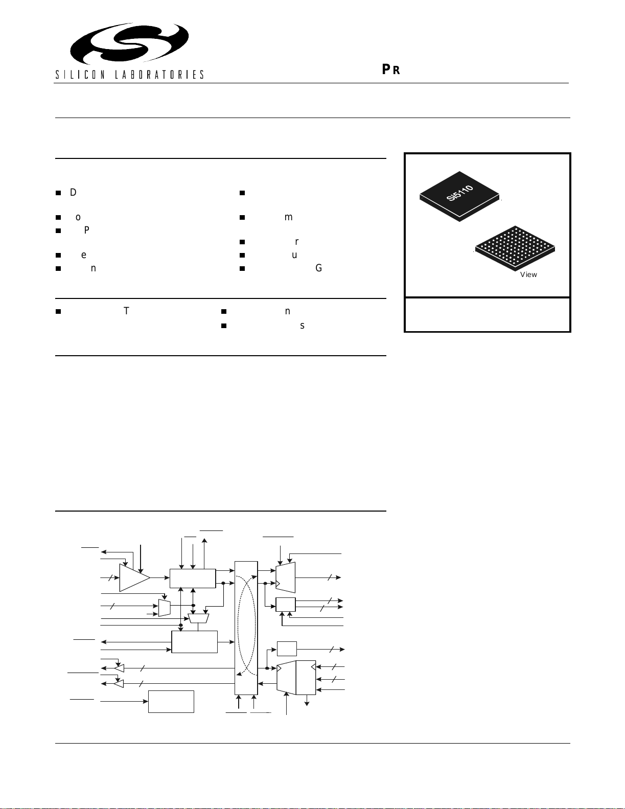
Si5110
:0
T
B
Bottom View
PRELIMINA RY DATA SHEET
SiPHY™ OC-48/STM-16 SONET/SDH TRANSCEIVER
Features
Complete low power, high speed, SONET/SDH transceiver with
integrated limiting amp, CDR, CMU, and MUX/DEMUX
Data Rates Supported:
OC-48/STM-16 and 2.7 Gbps FEC
Low Power Operation 1.0 W (typ)
DSPLL™ Based Clock Multiplier Unit
w/ Selectable Loop Filter Bandwidths
Integrated Limiting Amplifier
Diagnostic and Line Loopbacks
SONET Compliant Loop Timed
Operation
Programmable Slicing Level and
Sample Phase Adjustment
LVDS Parallel Interfa ce
Single Supply 1.8 V Ope ratio n
11 x 11 mm B GA Package
Applications
Sonet/SDH Transmission
Systems
Optical Transc eiv e r Mo dules
Sonet/SDH Test Equipment
Si5110
Ordering Information:
See pa ge2 3.
Description
The Si5110 is a complete low-power transceiver for high-speed serial
communication systems operating between 2.5 Gbps and 2.7 Gbps. The receive
path consists of a fully integrated lim iting amplifier, clock and data recover y unit
(CDR), and 1:4 deserializer. The transmit path combines a low jitter clock
multiplier unit (CMU) with a 4:1 serializer. The CMU uses Silicon Laboratories’
™
DSPLL
technology to provide superior jitter performance while reducing design
complexity by eliminating external loop filter components. To simplify BER
optimization in long haul applications, programmable slicing, and sample phase
adjustment are supported.
The Si5110 operates from a single 1.8 V supply over the industrial temperature
range (–40°C to 85°C).
Functional Block Diagram
LOS
LOSLVL
RXDIN
REFSEL
REFCLK
LPTM
REFRATE
TXLO L
BWSEL
TXCLKDSBL
TXCLKOUT
TXSQLCH
TXDOUT
RESET
SLICELVL
2
Limiting
AMP
2
TXCLK4IN
2
2
PHASEADJ
RESET
Control
LTR
CDR
DSPLL
TX CMU
RXLOL
tm
Loopback Control
DLBKLLBK
RXSQLCH
1:4
÷
÷
4:1
TXMSBSEL
DEMUX
MUX
8
2
2
FIFO
FIFOERR
2
2
8
RXMSBSEL
RXDOUT[3
RXCLK1
RXCLK2
RXCLK2DIV
RXCLK2DS
TXCLK4OU
TXCLK4IN
TXD IN[3:0]
FIFORST
Preliminary Rev. 0.41 8/ 01 Copyright © 2001 by Silicon Labora tories Si5110-DS041
This in formation applies to a product under devel opment. I ts characteristics and specifications are subject to change without notice.
Page 2

Si5110
2 Preliminary Rev. 0.41
Page 3

Si5110
TABLE OF CONTENTS
Section Page
Electrical Specifications . . . . . . . . . . . . . . . . . . . . . . . . . . . . . . . . . . . . . . . . . . . . . . . . . 4
Functional Description . . . . . . . . . . . . . . . . . . . . . . . . . . . . . . . . . . . . . . . . . . . . . . . . . . 11
Receiver . . . . . . . . . . . . . . . . . . . . . . . . . . . . . . . . . . . . . . . . . . . . . . . . . . . . . . . . . . . . . . 11
Limiting Amplifier . . . . . . . . . . . . . . . . . . . . . . . . . . . . . . . . . . . . . . . . . . . . . . . . . . . . 11
Clock and Data Recovery (CDR) . . . . . . . . . . . . . . . . . . . . . . . . . . . . . . . . . . . . . . . . 12
Deserialization . . . . . . . . . . . . . . . . . . . . . . . . . . . . . . . . . . . . . . . . . . . . . . . . . . . . . . 12
Auxiliary Clock Output . . . . . . . . . . . . . . . . . . . . . . . . . . . . . . . . . . . . . . . . . . . . . . . . 12
Data Squelch . . . . . . . . . . . . . . . . . . . . . . . . . . . . . . . . . . . . . . . . . . . . . . . . . . . . . . . 12
Transmitter . . . . . . . . . . . . . . . . . . . . . . . . . . . . . . . . . . . . . . . . . . . . . . . . . . . . . . . . . . . . 13
DSPLL™ Clock Multiplier Unit . . . . . . . . . . . . . . . . . . . . . . . . . . . . . . . . . . . . . . . . . . 13
Serialization . . . . . . . . . . . . . . . . . . . . . . . . . . . . . . . . . . . . . . . . . . . . . . . . . . . . . . . . 13
Loop Timed Operation . . . . . . . . . . . . . . . . . . . . . . . . . . . . . . . . . . . . . . . . . . . . . . . . . . . 14
Diagnostic Loopback . . . . . . . . . . . . . . . . . . . . . . . . . . . . . . . . . . . . . . . . . . . . . . . . . . . . 14
Bias Generation Circuitry . . . . . . . . . . . . . . . . . . . . . . . . . . . . . . . . . . . . . . . . . . . . . . . . 14
Voltage Reference Output . . . . . . . . . . . . . . . . . . . . . . . . . . . . . . . . . . . . . . . . . . . . . 14
Transmit Differential Output Circuitry . . . . . . . . . . . . . . . . . . . . . . . . . . . . . . . . . . . . . . 15
Si5110 Pinout: 99-Pin BGA . . . . . . . . . . . . . . . . . . . . . . . . . . . . . . . . . . . . . . . . . . . . . . . 16
Pin Descriptions: Si5110 . . . . . . . . . . . . . . . . . . . . . . . . . . . . . . . . . . . . . . . . . . . . . . . . . 18
Ordering Guide . . . . . . . . . . . . . . . . . . . . . . . . . . . . . . . . . . . . . . . . . . . . . . . . . . . . . . . . . 23
Package Outline . . . . . . . . . . . . . . . . . . . . . . . . . . . . . . . . . . . . . . . . . . . . . . . . . . . . . . . . 24
Contact Information . . . . . . . . . . . . . . . . . . . . . . . . . . . . . . . . . . . . . . . . . . . . . . . . . . . . . 26
Preliminary Rev. 0.41 3
Page 4
Si5110
t
t
Electrical Specifications
Table 1. Recommended Operating Condit ions
Parameter Symbol Test Condition
Ambient Temperatur e T
LVTTL Output Supply Voltage V
Si5110 Supply Voltage V
*Note: All minimum and maximum specifications are guaranteed and apply across the rec om me nded operating conditions.
T ypical values apply at nominal supply voltages and an operating temper ature of 25°C unless otherwise st ated.
A
DD33
DD
*
Min
Typ
–40 25 85 °C
1.71 — 3.47 V
1.71 1.8 1.89 V
Max
*
Unit
V
SIGNAL +
Differential
I/Os
V
ICM
SIGNAL –
, V
OCM
V
IS
Single Ended Voltage
(SIGNAL +) – (SIGNAL –)
Differential
Voltage Swing
VID,VOD (V
= 2VIS)
ID
Differential Peak-to-Peak Voltage
t
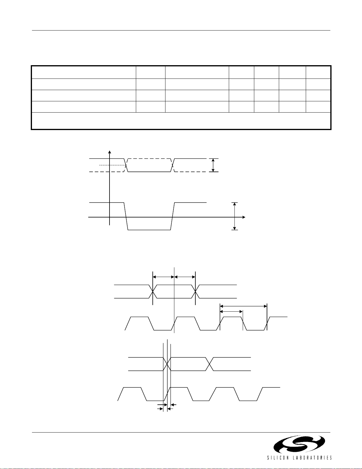
Figure 1. Differential Voltage Measurement
(RXDIN, RXDOUT, RXCLK1, RXCLK2, TXDIN, TXDOUT, TXCLKOUT, TXCLK4OUT, TXCLK4IN)
TXDOUT,
TXDIN
TXCLKOUT,
TXCLK4IN
RXDOUT
RXCLK1
su
hd
t
t
CH
CP
t
t
cq1
cq2
Figure 2. Data to Clock Delay
4 Preliminary Rev. 0.41
Page 5
Si5110
All
80%
Differential
IOs
t
F
t
R
20%
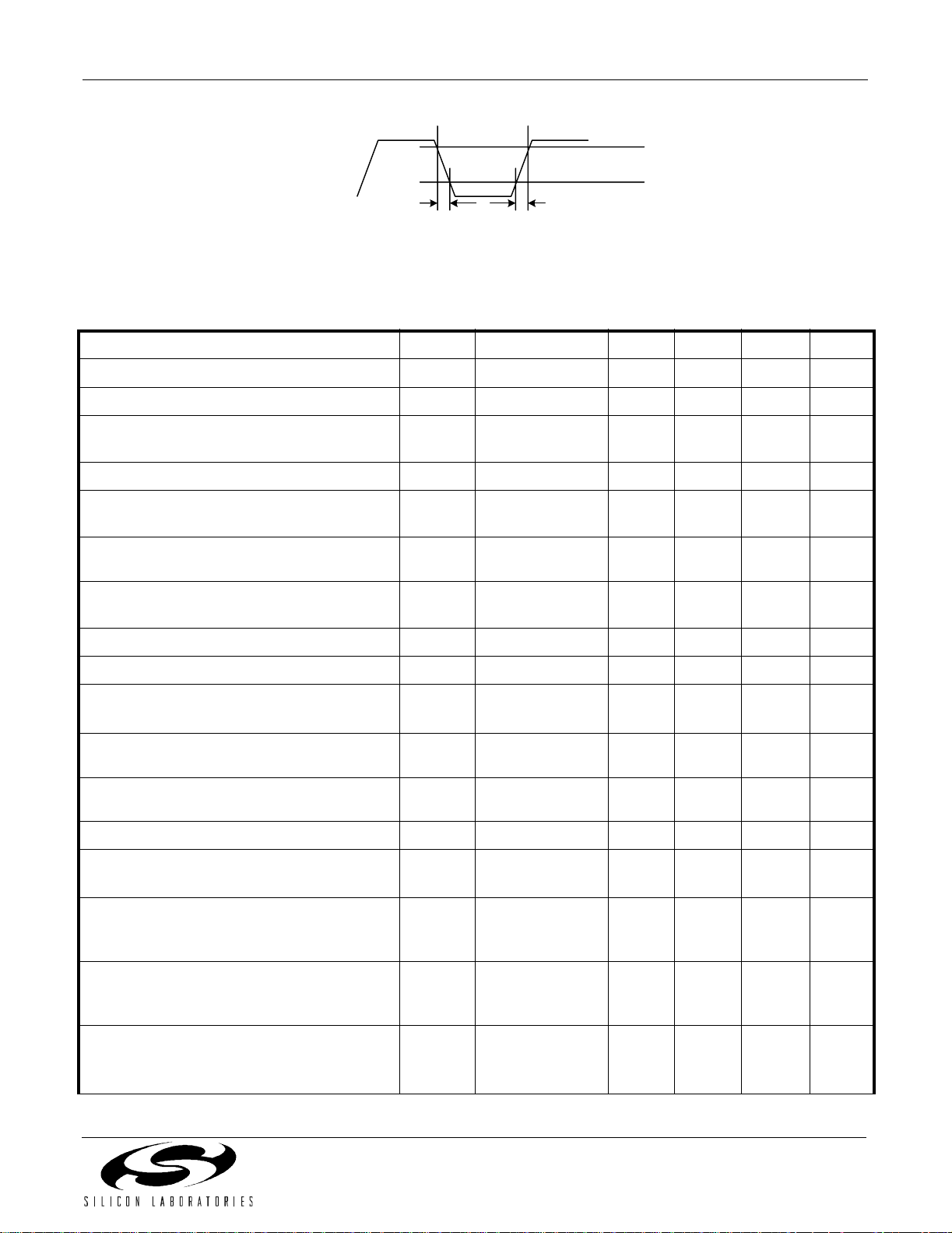
Figure 3. I/O Rise/Fall Times
Table 2. DC Characteristic s
(VDD = 1.8 V ±5% , TA = –40°C to 85°C)
Parameter Symbol Test Condition Min Typ Max Unit
Supply Current I
Power Dissipation P
Voltage Reference (VREF) V
Common Mode Input Voltage (RXDIN) V
Differential Input Voltage Swing (RXDIN) V
Common Mode Output Voltage
V
(TXDOUT, TXCLKOUT)
Differential Output Voltage Swing
V
(TXDOUT, TXCLKOUT), Differential pk-pk
DD
D
REF
ICM
ID
OCM
OD
VREF driving
Ω load
10 k
See Figure 1 10 — 1.0 mV
See Figure 1 800 1000 1200 mV
—611TBDmA
—1.0TBDW
1.21 1.25 1.29 V
TBD 0.1 TBD V
(pk-pk)
.8 0.9 1.0 V
(pk-pk)
L VPECL Input Voltage HIGH (REFCLK) V
L VPECL Input Voltage LOW (REFCLK) V
L VPECL Input Voltage Swing,
Differential pk-pk (REFCLK)
LVPECL Internally Gene rated Input Bias
(REFCLK)
L VDS Input High Voltage (TXDIN,
TXCLK4IN)
L VDS Input Low Voltage (TXDIN, TXCLK4IN) V
L VDS Input Voltage, Single Ended pk-pk
V
(TXDIN, TXCLK4IN)
LVDS Output High Voltage
V
(RXDOUT, RXCLK1, RXCLK2,
TXCLK4OUT)
LVDS Output Low Voltage
V
(RXDOUT, RXCLK1, RXCLK2,
TXCLK4OUT)
L VDS Output Voltage, Differential pk-pk
V
(RXDOUT, RXCLK1, RXCLK2,
TXCLK4OUT)
V
V
V
ISE
OH1
OL1
OSE
IH
IL
ID
IB
IH
IL
1.975 2.3 2.59 V
1.32 1.6 1.99 V
Figure 1 250 — 2400 mV
1.6 1.95 2.3 V
——2.4V
0.0 — — V
100 — 600 mV
100 Ω Load
TBD — 1.475 mV
Line-to-Line
100 Ω Load
0.925 — TBD V
Line-to-Line
100 Ω Load
500 — 800 mV
Line-to-Line,
Figure 1
(pk-pk)
(pk-pk)
(pk-pk)
Preliminary Rev. 0.41 5
Page 6
Si5110
Table 2. DC Characteristic s (Con tinued)
(VDD = 1.8 V ±5% , TA = –40°C to 85°C)
Parameter Symbol Test Condition Min Typ Max Unit
L VDS Common Mode Voltage
(RXDOUT, RXCLK1, RXCLK2,
TXCLK4OUT)
Input Impedance (TXDIN, TXCLK4I N,
REFCLK, RXDIN)
Output Short to GND
(RXDOUT, RXCLK1, RXCLK2,
TXCLK4OUT, TXDOUT, TXCLKOUT)
Output Short to V
DD
(RXDOUT, RXCLK1, RXCLK2,
TXCLK4OUT, TXDOUT, TXCLKOUT)
LVTTL Input Voltage Low
(RXMSBSEL, RXCLK2DIV, RXCLK2DSBL,
RXSQLCH
TXCLKDSBL, FI FOR ST, TXSQL CH
BWSEL, TXMSBSEL, DLBK
, REFSEL, LTR, RESET, MODE16
,
, LLBK, LPTM)
LVTTL Input Voltage High
(RXMSBSEL, RXCLK2DIV, RXCLK2DSBL,
RXSQLCH
TXCLKDSBL, FI FOR ST, TXSQL CH
BWSEL, TXMSBSEL, DLBK
, REFSEL, LTR, RESET, MODE16
,
, LLBK, LPTM)
LVTTL Input Low Current
(RXMSBSEL, RXCLK2DIV, RXCLK2DSBL,
RXSQLCH
TXCLKDSBL, FI FOR ST, TXSQL CH
BWSEL, TXMSBSEL, DLBK
, REFSEL, LTR, RESET, MODE16
,
, LLBK, LPTM)
LVTTL Input High Current
(RXMSBSEL, RXCLK2DIV, RXCLK2DSBL,
RXSQLCH
TXCLKDSBL, FI FOR ST, TXSQL CH
BWSEL, TXMSBSEL, DLBK
, REFSEL, LTR, RESET, MODE16
,
, LLBK, LPTM)
L VTTL Input Impedance
(RXMSBSEL, RXCLK2DIV, RXCLK2DSBL,
RXSQLCH
TXCLKDSBL, FI FOR ST, TXSQL CH
BWSEL, TXMSBSEL, DLBK
, REFSEL, LTR, RESET, MODE16
,
, LLBK, LPTM)
LVTTL Output Voltage Low
(LOS
, RXLOL, FIFOERR, TXL OL)
V
CM
R
I
SC(–)
I
SC(+)
V
IL2
V
IH2
I
IL
I
IH
R
V
OL2
1.125 — 1.275 V
IN
Each input to
42 50 58 Ω
common mode
—25TBDmA
TBD –100 — µA
VDD33 = 3.3 V — — 0.8 V
VDD33 = 1.8 V — — 0.7
VDD33 = 3.3 V 2.0 — — V
VDD33 = 1.8 V 1.7
——10µA
——10µA
IN
10 — — kΩ
VDD33 = 1.8 V — — 0.4 V
VDD33 = 3.3 V — — 0.4
LVTTL Output Voltage High
(LOS
, RXLOL, FIFOERR, TXL OL)
6 Preliminary Rev. 0.41
V
OH2
VDD33 = 1.8 V 1.4 — — V
VDD33 = 3.3 V 2.4 — —
Page 7
Si5110
Table 3. AC Characteristics (RXDIN, RXDOUT, RXCLK1, RXCLK2)
(VDD = 1.8 V ±5% , TA = –40°C to 85°C)
Parameter Symbol Test Condition Min Typ Max Unit
Output Clock Frequency
f
clkout
See Figure 2 — 622 667 MHz
(RXCLK1)
Duty Cycle (RXCLK1, RXCLK2) tch/tcp, Figure 2 45 — 5 5 %
Output Rise and Fall Times
t
R,tF
Figure 3 — 50 — ps
(RXCLK1, RXCLK2, RXDOUT)
Data Invalid Prior to RXCLK1 t
Data In valid A fter RXCL K1 t
cq1
cq2
Input Return Loss (RXIN) 100 kHz–2.5 GHz
Figure 2 — — 200 ps
Figure 2 — — 200 ps
2.5 GHz–4.0 GHz
18.7
TBD
—
—
—
—
dB
dB
Slicing Adjust Dynam ic Range SLICELVL = 200–800 mV –20 — 20 mV
Slicing Level Offset
1
SLICELVL = 200–800 mV –500 — 500
µV
(referred to RXDIN)
Slicing Level Accuracy VSLICE –5 — 5 %
Sampling Phase Adjustment
2
PHASEADJ = 200–800 mV –22.5° — 22.5°
LOS Threshold Dynamic Range LOSLVL = 200–800 m V 10 — 50 mV
pk-pk
LOS Threshold Offset
3
LOSLVL = 200–800 mV –500 — 500
µV
(referred to RXDIN)
LOS Threshold Accuracy VLOS –5 — 5 %
Note:
1. Slice level (referred to RXDIN) is calculated as follows: VSLICE = (SLICE_LVL – 0.4
2. Sample Phase Offset is calcul ated as follows: PHASE OFFSET = 22.5
3. LOS Threshold voltage (referred to RXDIN) is calculated as follows: VLOS = 30 mV + (LOS_LVL – 0.4
°(PHASEADJ – 0.4
VREF)/15.
VREF)/0.3
VREF)/15.
Preliminary Rev. 0.41 7
Page 8
Si5110
Table 4. AC Characteristics (TXCLK4OUT, TXCLK4IN, TXCLKOUT, TXDIN, TXDOUT)
(V
1.8 V ±5%, TA = –40°C to 85°C)
DD =
Parameter Symbol Test Condition Min Typ Max Unit
TXCLKOUT Frequency f
clkout
Figure 2 — 2.5 2.7 GHz
TXCLKOUT Duty Cycle tch/tcp, Figure 2 45 — 55 %
Output Rise Time
t
R
Figure 3 — 25 — ps
(TXCLKOUT, TXDOUT)
Output Fall Time
t
F
Figure 3 — 25 — ps
(TXCLKOUT, TXDOUT)
TXCLKOUT Setup to TXDOUT t
TXCLKOUT Hold From TXDOUT t
su
hd
Output Return Loss 100 kHz–2. 5 GHz
TXCLK4OUT Frequency f
CLKIN
Figure 2 25 — — ps
Figure 2 25 — — ps
2.5 GHz–4.0 GHz
TBD
TBD
—
—
—
—
— 622 667 MHz
dB
dB
TXCLK4OUT Duty Cycle tch/tcp, Figure 2 40 — 60 %
TXCLK4OUT Rise & Fall Times t
TXDIN Setup to TXCLK4IN t
TXDIN Hold from TXCLK4IN t
TXCLK4IN Frequency f
R,tF
DSIN
DHIN
CLKIN
100 — 300 ps
— — 300 ps
— — 300 ps
— 622 667 MHz
TXCLK4IN Duty Cycle tch/tcp, Figure 2 40 — 60 %
TXCLK4IN Rise & Fall Times t
R,tF
100 — 300 ps
8 Preliminary Rev. 0.41
Page 9

Si5110
Table 5. AC Character i sti cs (Receiver PLL)
(VDD = 1.8 V ±5% , TA = –40°C to 85°C)
Parameter Symbol Test Condition Min Typ Max Unit
Jitter Tolerance J
TOL(PP)
f = 600 Hz 15 30 — UIpp
f = 6000 kHz 1.5 3.0 — UIpp
f = 100 kHz 1.5 3.0 — UIpp
f = 1 MHz 0.15 0.3 — UIpp
Acquisition Time T
Input Reference Clock Frequency RC
AQ
FREQ
REFRAT E= 1 — 155 167 MHz
REFRATE = 0 — 78 83 MHz
Reference Clock Duty Cycle RC
Reference Clock Frequency
RC
DUTY
TOL
Tolerance
Frequency Difference at which
LOL TBD 600 1000 ppm
Receive PLL goes out of Lock
(REFCLK compared to the
divided down VCO clock)
Frequency Difference at which
LOCK TBD 300 TBD ppm
Receive PLL goes into Lock
(REFCLK compared to the
divided down VCO clock)
Note: Bellcore specifications: GR-1377-CORE, Issue 5, December 1998.
——20 µs
40 50 60 %
–100 — 100 ppm
Table 6. AC Characteristics (Transmitter Clock Multiplier)
(VDD = 1.8 V ±5% , TA = –40°C to 85°C)
Parameter Symbol Test Condition Min Typ Max Unit
Jitter Generation J
Jitter Transfer Bandwidth J
GEN(rms)
BW
Jitter Transfer Peaking — 0.05 0.1 dB
Acquisition Time T
Input Reference Clock Frequency RC
Input Reference Clock Duty
RC
AQ
FREQ
DUTY
Cycle
Input Reference Clock Frequency
RC
TOL
Tolerance
Note: Bellcore specifications: GR-1377-CORE, Issue 5, December 1998.
PRBS 23 0.005 TBD UI
BWSEL = 0 — — 6 kHz
BWSEL = 1 — — 2 5 kHz
Valid REFCLK — — 20 µs
REFRAT E= 1 — 155 167 MHz
REFRATE = 0 — 78 84 MHz
40 — 60 %
–100 — 100 ppm
RMS
Preliminary Rev. 0.41 9
Page 10

Si5110
Table 7. Ab so l u te M aximu m R atings
Parameter Symbol Value Unit
DC Supply Voltage V
LVTTL Input Voltage V
Differential Input Voltages V
DD
DD33
DIF
–0.5 to TBD V
–0.5 to 3.6 V
–0.3 to (VDD+ 0.3) V
Maximum Current any output PIN ±50 mA
Operating Junction Temperature T
Storage Temperature Range T
Package Temperature
JCT
STG
–55 to 150 °C
–55 to 150 °C
275
°C
(soldering 10 seconds )
ESD HBM Toler anc e (100 pf, 1.5 k
Note: Permanent device damage m ay occur if the above Absolute Ma ximum Ratings are exceeded. Functional operation
should be restricted to the conditions as specified in the operational sections of this data sheet. Exposur e to absolute
maximum rating conditions for extende d periods may affect device reliability.
Ω)TBDV
Table 8. Thermal Ch ar acteristi cs
Parameter Symbol Test Condition Value Unit
Thermal Resistance Junction to Ambient ϕ
JA
Still Air 38 ° C/W
10 Preliminary Rev. 0.41
Page 11

Functional Description
V
0.4xVREF–
V
0.4xVREF–
Si5110
The Si5110 transceiver is a low power, fully integrated
serializer/deserializer that prov i des s ignificant mar gin to
all SONET/SDH jitter specifications. The device
operates from 2.5–2.7 Gbps making it suitable for OC48/STM-16, and OC-48/STM-16 applications that use
15/14 forward error correction (FEC) coding. The low
speed receive/transmit interface uses a low power
parallel LVDS interface.
Receiver
The receiver within the Si5110 includes a precision
limiting amplifier, jitter tolerant cloc k and data recovery
unit (CDR), and 1:4 demultiplexer. In addition,
programmable data slicing and sampling phase
adjustment are prov ided to suppo rt bit-error-rat e (BER)
optimization for long haul ap plications.
Limiting Amplifier
The Si5110 incorporates a high sensitivity limiting
amplifier with sufficient gain to directly accept the output
of transimpedance amplifiers. High sensitivity is
achieved by using a digital calibration algorithm to
cancel out amplifier offsets. This algorithm achieves
superior offset cancellation by using statistical
averaging to remove noise that may degrade more
traditional calibra tion routines.
The limiting amplifier provides sufficient gain to fully
saturate with input signals that are less than 10 mV
peak-to-peak differentia l. In addition, input signals that
exceed 1 V peak- to-peak differential will not cau se any
performance degradation.
Loss-of-Signal (LOS) Detection
The limiting am plifie r incl udes circ uitry t hat g enerates a
loss-of-signal (LOS) alarm when the input signal
amplitude on RXDIN falls below an externally controlled
threshold. The Si5110 can be configured to drive the
LOS
output low when the differential input amplitude
drops below a threshold s et b etween ~8 m V a nd 50 mV
pk-pk differential. Approximately 3 dB of hysteresis
prevents unnecessary switching on LOS
The LOS threshold is set by applying a voltage between
0.20 V and 0.80 V to the LOSLVL input. The voltage
present on LOSLVL maps to an input signal threshold
as follows:
()
LOSLVL
V
V
is the differential pk-pk LOS threshold referred to
LOS
the RXDIN input, V
---------------------------------------------------------------
LOS
LOSLVL
15
is the voltage applied to the
LOSLVL pin, and VREF is reference voltage output on
.
30 mV+=
the VREF pin.
The LOS detection circuitry is disabled by tieing the
LOSLVL input to the supply (VDD). T his fo rces t he LOS
output high.
Slicing Level Adjustment
To support applications that require BER optimization,
the limiting amplifier provides circuitry that supports
adjustment of t he 0/1 decision threshold (slicing l evel)
over a range of ±20 m V when referred to the interna lly
biased RXDIN input . The slicing le vel is set by applying
a voltage between 0.20 V and 0.80 V t o the SLICELVL
input. The voltage present on S LICELVL sets the slicing
level as follow s:
()
SLICE
-----------------------------------------------------------
LEVEL
=
15
V
LEVEL
V
SLICE
V
is the slicing l evel referred to the RX DIN input,
is the voltage applied to the SLICE_LVL pin, and
VREF is reference voltage outpu t on the VREF pin.
The slicing lev el adjustment may be disabled by tiei ng
the SLCLVL input to the supply (VDD). When slicing is
disabled, the slicing offset is set to 0.0 V relative to
internally biased input common mode voltage for
RXDIN.
Clock and Data Recovery (CDR)
The Si5110 uses an integrated CDR to recover clock
and data from a non-return to zero (NRZ) signal input on
RXDIN. The recovered data clock is used to regenerate
the incoming data by sam pling the output of the l imiting
amplifier at the center of the NRZ bit period. The
recovered cloc k and data is then deserialized by a 1:4
demultiplexer and output via a LVDS compatible low
speed interface (RXDOUT[3:0], RXCLK1, and
RXCLK2).
Sample Phase Adjustment
In applications where it is not desirable t o recover d ata
by sampling in the center of the data eye, the Si5110
supports adjustment of the CDR sampling phase across
the NRZ data period. When sample phase adjustment is
enabled, the sampling instant used for data recovery
can be moved over a range of ±22.5
center of the incoming NRZ bit period. Adjustment of the
sampling phase is de sirable when data eye distortions
are introduced by the transmission medium.
The sample phas e is s et by applying a voltage b etween
0.20 V and 0.80 V t o t he P H A SEADJ input. The voltage
present on PHASEADJ maps to sam ple phas e offset as
follows:
° relative to the
Preliminary Rev. 0.41 11
Page 12

Si5110
22.5°xV
PhaseOffset
Phase Offset is the s ampli ng offset in deg rees from the
center of the data eye, V
the PHASEADJ pin, and VREF is reference voltage
output on the VREF pin. A positive phase offset will
adjust the sampli ng point to lead the de fault sampling
point in the center of the data eye, and a negative phase
offset will adjust the sampling point to lag the default
sampling point.
Data recovery using a sampling phase offset is disabled
by tieing t he PHASEADJ input to the supply (VDD). This
forces a phase offset of 0
Receiver Lock Detect
The Si5110 provides lock-detec t circuitry that indicates
whether the PLL has achieved frequenc y lock with the
incoming data. This circuit compares the frequen cy of a
divided down version of the recovered clock with the
frequency of the s upplied reference c lock (REFC LK). If
the recovered clo ck freque ncy deviat es from that o f the
reference clock by the amount specified in Table 5 on
page 9, the PLL is de cl ared out of lo ck, and the loss- oflock (RXLOL
attempt to reacquire lock with the incoming data stream.
During reacquisition, the recovered clock frequency
(RXCLK1 and RXCLK2) will drift over a ±1000 ppm
range relative to the supplied reference clock. The
RXLOL
clock frequency is w ithin t he REF CLK fre quency by t he
amount specified in Table 5 on page 9.
Lock-to-Reference
In applications where it is desirable t o maintain a stable
output clock during an alarm condition like loss-ofsignal, the lock-t o-referen ce input (LTR
force a stable output clock . When LTR
CDR is prevented from acquiring the data signal and the
CDR will lock the RXCLKOUT1 and RXCLKOUT2
outputs to the provided REFCLK. In typical applications,
the LOS
stable output clock.
) pin is assert ed. In this state, the PLL will
output will remain asserted until the recovered
output would be tied to the LTR input to force a
-------------------------------------------------------------------------------
=
PHASE
is the voltage applie d to
PHASE
o
to be used for data recovery.
0.4xVREF–()
0.30
) can be used to
is asserted, the
Deserialization
The Si5110 uses a 1:4 demultiplexer to de serialize the
high speed input. The deserialized data is output on a 4bit parallel data bus, RXDOUT[3:0], synchronous with
the rising edge of RXCLK1. This clock output is deriv ed
by dividing down the recovered clock by a factor of 4.
Serial In put to Parallel Output Relatio nship
The Si5110 provides the capability to select the order in
which the receiv ed serial data is m apped to the parallel
output bus RXDOUT[3:0]. The mappi ng of the receive
bits to the output data word is controlled by the
RXMSBSEL input. If RXMSBSEL is tied low, the first bit
received is output on RXDOUT0 and the followi ng bits
are output in order on RXDOUT1 throug h RXDOUT3. If
RXMSBSEL is tied high, the fir st bit received is output
on RXDOUT3, and the following bits are output in order
on RXDOUT2 through RXDOUT0.
Auxiliary Clock Output
To support the widest range of system timing
configurations, a second clock output is provided on
RXCLK2. This output can be configured to provide a
clock equal to either the parallel output word rate or
1/4th the output word rate. The divide factor used to
generate RXCLK2 is controlled via the RXCLKDIV2
input as described in the Pin Description table. In
applications which do not use RXCLK2, this output can
be powered down by forcing the RSCLK2DSBL input
high.
Data Squelch
During some system error conditions, such as LOS, it
may be desirable to force the receive data output to
zero in order to avoid propagation of erroneous data
into the downstream processing circuitry. In these
applications, the Si5110 provides a data squelching
control input, RXSQLCH
the data on RXDOUT will be forced to 0. Data squelch is
disabled if the device is operating in diagnostic
loopback mode (DLBK
. When this input is active low,
= 0).
Transmitter
The transmitter consists of a low jitter, clock multiplier
unit (CMU) with a 4:1 serializer. The CMU uses a
phase-locked loop (PLL) architect ure based on Silic on
Laboratories’ proprietary DSPLL
technology is u sed t o generate ultra-low j itter cloc k a nd
data outputs that provide significant margin to the
SONET/SDH specifications. The DSPLL architecture
also utilizes a digitally implemented loop filter that
eliminates the need for external loop f ilter components.
As a result, sensit iv e nois e c oupling nodes that typi ca lly
cause degraded jitter performance in crowded PCB
environments are removed.
The DSPLL also reduces the complexity and
performance requirements of reference clock
distribution strategies for OC-48/STM-16 optical port
cards. This is possible because the DSPLL provides
selectable wideband and narr owband loop filter setti ngs
that allow the user to set the jitter attenuation
characteristics o f the CMU to accommodat e reference
clock sources that have a high jitter content. Unlike
traditional analog PLL implementations, the loop filter
™
technology. This
12 Preliminary Rev. 0.41
Page 13

Si5110
bandwidth is controlled by a digital filter inside the
DSPLL and can be changed without any modification to
external components.
DSPLL™ Clock Multiplier Unit
The Si5110’s clock multiplier unit (CMU) uses Silicon
Laboratories proprietary DSPLL techn ology to gene rate
a low jitter, high frequency clock source capable of
producing a high speed serial clock and data output with
significant margin to the SONET/SDH specifications.
This is achieved by using a digital signal processing
(DSP) algorithm to replace the loop filter commonly
found in analog PLL design s. This algorithm processes
the phase detector error term and generates a digital
control value to adjust the frequency of the voltage
controlled oscillator (VCO). Because exter nal loop filter
components are not required, sensitive noise entry
points are eliminated, thus making the DSPLL less
susceptible to board-level noise sources. Therefore,
SONET/SDH jitter compliance is easier to attain in the
application.
Programm able Loop Filt er B andwidth
The digitally implemented loop filter allows for two
bandwidth settings that provide either wideband or
narrowband jitter transfer characteristics. The filter
bandwidth is selected via the B WSEL control input. In
traditional PLL impleme ntations, changing the loop filter
bandwidth would require changing the values of
external loop filter components.
In narrowband mode, a loop filter cutoff of 6 kHz is
provided. This set ting makes the Si5110 more tolerant
to jitter on the reference c lock source. As a result, the
complexity of the clock distribution circuitry used to
generate the physical layer reference clocks can be
simplified without compromising jitter margin to the
SONET/SDH specification.
In wideband mode, the loop filter provides a cutoff of
25 kHz. T his setting is desirable in applications where
the reference clock is provided by a low jitter source like
the Si5364 Clock Synchronization IC or Si5320
Precision Clock Multiplier/Jitter Attenuator IC. This
allows the DSPLL to more closely track the precision
reference source resulting in the best possible jitter
performance.
Serialization
The Si5110 includes serialization circuitry that combines
a FIFO with a parallel t o serial shi ft register. Low speed
data on the parallel 4-bit input bus, TXDIN[3:0], is
latched into the FIFO on the rising edge of TXCLK4 IN.
The data in the FIFO is loaded int o the shift register by
TXCLK4OUT, an output clock that is produced by
dividing down the high speed transmit clock,
TXCLKOUT , by a factor of 4. The high-speed serial data
stream is clocked out of the shift register by
TXCLKOUT. The TXCLK4OUT clock output is provided
to support d ata wor d transf ers be tween t he S i5110 and
upstream devices using a counter cloc king s cheme.
Input FIFO
The Si5110 integrates a FIFO to decouple data
transferred into the FIFO via TXCLK4IN from data
transferred into the shift register via TXCLK4OUT. The
FIFO is e ight parallel words deep a nd accommodates
any static phase delay that m ay be intr oduced betwe en
TXCLK4OUT and TXCLK4IN in counter clocking
schemes. Further, the FIFO will accom modate a phase
drift or wander between TXCLK4IN and TXCLK4OUT of
up to three parallel data words.
The FIFO circuitry indicates an overflow or underflow
condition by asser ting FIFOERR high. This out put can
be used to recenter the FIFO read/write pointers by
tieing it di rectly to the FIFORST inp ut. The Si5110 will
also recenter the rea d/write pointers after the device’s
power on reset, external reset via RESET
time the DSPLL transitions from an out of lock state to a
locked state (TXLOL
Parallel Inp ut To Serial Output Relationship
The Si5110 provides the capability t o selec t the order in
which data on the parallel input bus is transmitted
serially. Data on this bus can be transmitted MSB first or
LSB first depending on the setting of TXMSBSEL. If
TXMSBSEL is tied low, TXDIN0 is transmitted first
followed in order by TXDIN1 through TXDIN3. If
TXMSBSEL is tied high, TXDIN3 is transmitted first
followed in order by TXDIN2 through TXDIN0. This
feature simpl ifies board routing when ICs are mounted
on both sides of the PCB.
Transmit Data Squelch
To pre vent the transmis sion of corrupted data into the
network, the Si5110 provides a control pin that can be
used to forc e TXDOUT to 0. By driving TXSQLCH
the high speed serial ou tput, TXDOUT will be forced to
0. Transmit data squelching is disabled when the device
is in line loopback mode (LLBK
Clock Disable
The Si5110 provides a clock disable pin, T XCLKDSBL,
that is used to disable the high -speed serial data clock
output, TXCLKOUT. When the TXCLKDSBL pin is
asserted, the positive and negative terminals of
CLKOUT are tied to 1.5 V through 50
resistors. This feature is used to reduce power
consumption in applications that do not use the high
speed transmit data clock.
transitions from low to high).
=0).
, and each
low,
Ω on-chip
Preliminary Rev. 0.41 13
Page 14

Si5110
Loop Timed Operation
The Si5110 can be configured to pr ovide SONET/SDH
compliant loop timed operation. When LPTM is asserted
high, the transmit c lock and data timing is der ived from
the recovered clock output by the CDR. This is achieved
by dividing down the reco vered clock and using it as a
reference source for the transmit CMU. This will
produce a transmit clock and data that ar e lock ed to the
timing recovered from the received data path. In this
mode, a narrow band loop filter setting is
recommended.
Diagnostic Loopback
The Si5110 supports diagnostic loopback which
establishes a loopback path from the serializer output to
the deserializer input. This provides a mechanism for
looping back data input via the low speed transmit
interface TXDIN to the low speed receive data interface
RXDOUT. This mode is enabled by forcing DLBK
low.
Line Loopback
The Si5110 supports line loopback which establis hes a
loopback path from the high speed receive input to the
high speed transmit output. This prov ides a mechan ism
for looping back the high-speed clock and data
recovered from RXDIN to the transmit data output
TXDOUT and clock TXCLKOUT. This mode is enabled
by forcing LLBK
low.
Bias Generation Circuitry
The Si5110 makes use of two external resistors,
RXREXT and TXREXT, to set internal bias currents for
the receive and transmit sections of the Si5110. The
external resistors allows precise generation of bias
currents that significantly reduce power consumption.
The bias generation circuitry requires 3.09 k
resistors connected between RXREXT/TXREXT and
GND.
Ω (1%)
reference cloc k sour c es. The first c onf igur at ion uses an
externally provided reference clock that is input via
REFCLK. The second configuration uses the parallel
data clock, TXCLK4I N, as the ref erence clock source.
When using TXCLK4IN as the reference source, the
narrowband loop filter setting in the CMU may be
preferable to remove jit ter that may be present on the
data clock. The selection of reference clock source is
controlled via the REFSEL input.
The CMU in the Si5110’s transmit section multiplies up
the provided ref erence to the serial transm it data rate.
When the CMU has achieved lock with the selected
reference, the TXLOL
CDR in the receive section of the Si5110 uses a
reference clock to cent er the PLL frequenc y so that it is
close enough to the data f requenc y t o ac hieve lock with
the incoming data. When the CDR has locked to the
data, R XLOL
is driven high.
output will be driven high.The
Reset
The Si5110 is reset by holding the RESET pin low for at
least 1
pointers reset an d the digital control circuitry initializ es.
When RESET
the CMU will be calibrated.
Voltage Reference Output
The Si5110 provides an output voltage reference that
can be used by an external circuit to set the LOS
threshold, slicing lev el, or sampling phase adjustment.
One possible implementation would use a resistor
divider to set the control voltage for LOSLVL,
SLICELVL, or PHASEADJ. A second altern ative would
use a DAC to set the control voltage. Using this
approach, VRE F would be used to establish the range
of a DAC output. The reference voltage is nominally
1.25 V.
µs. When RESET is asserted low, the input FIFO
transitions high to start n or mal operat ion,
Reference Clock
The Si5110 is designed to operate with refere nce cl ock
sources that are either 1/16th or 1/32nd the desired
transceiver data rate. T he device will support operation
with data rates between ~2.5 Gbps a nd ~2.7 Gbps and
the reference clock should be scaled accordingly. For
example, to suppo rt 2.67 Gbps operation the ref erence
clock source would be approximately 83 MHz or
167 MHz. T he REFRATE input pin is used t o configure
the device for operation with one of the two suppo rted
reference clock submultiples of the data rate.
The Si5110 supports operation with two selectable
14 Preliminary Rev. 0.41
Page 15

Si5110
Transmit Differential Output Circuitry
The Si5110 utilizes a current-mode logic (CML) architecture to drive the high speed serial output clock and data on
TXCLKOUT and TXDOUT. An example of output termination with ac cou pling is shown in Figure 4. In applications
where direct dc cou pling is possibl e, the 0.1
swing of the CML architecture is list ed in Table 2 on page 5.
µF capacitors may be omitted. The differential peak- to-peak voltag e
50 Ω
1.5 V
50 Ω
24 mA
0.1 µF
0.1 µF
Zo = 50 Ω
Zo = 50 Ω
VDD
50 Ω
50 Ω
VDD
Figure 4. CML Output Driver Termination (TXCLKOUT, TXDOUT)
Preliminary Rev. 0.41 15
Page 16

Si5110
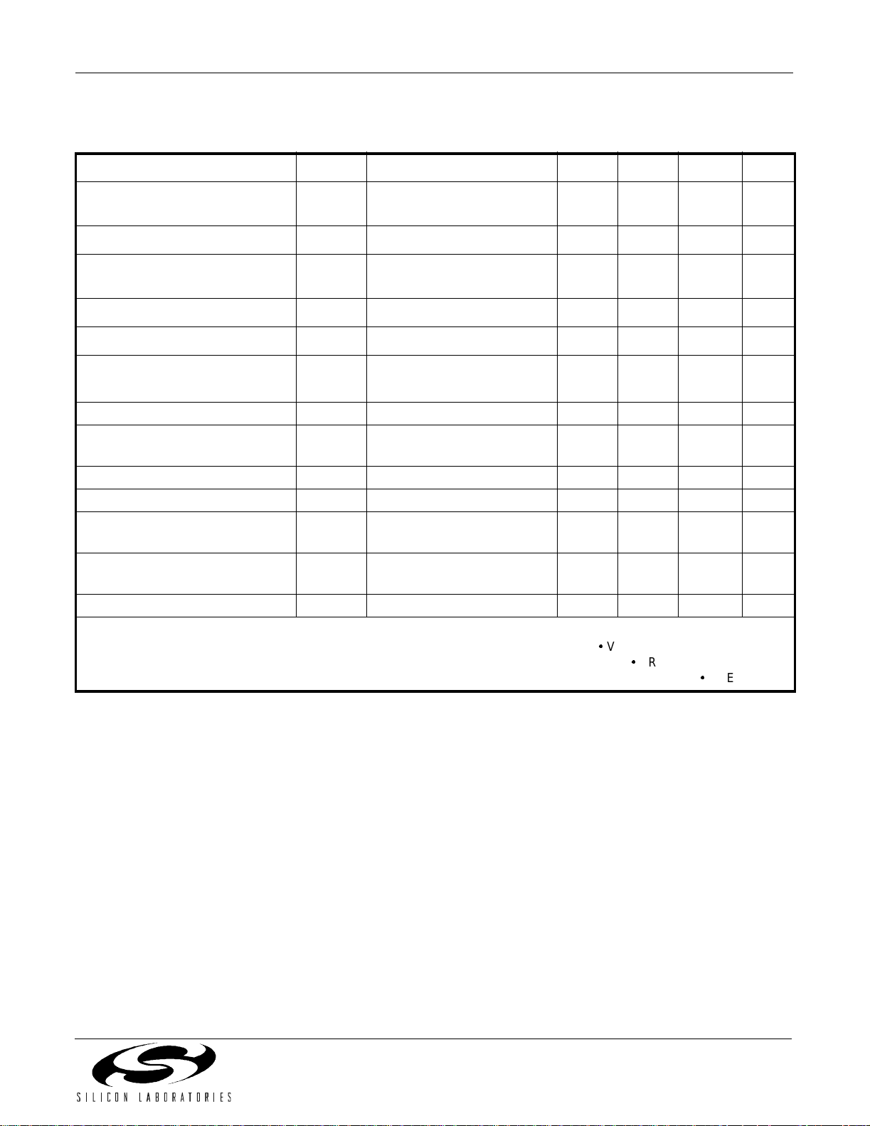
Si5110 Pinout: 99 BGA
110 9 78 65432
PHASEADJSLICELVLRXREXTRXSQLCHRSVD_GNDRXCLK[2]RXCLK[2]RXDOUT[1]RXDOUT[0]
RXDINGNDLOSLVLVREFNCRSVD_GNDRXCLK[1]RXCLK[1]RXDOUT[1]RXDOUT[0]
RXDINGNDRXLOLLTRRSVD_GNDRSVD_GNDRXCLK2DSBLRXCLK2DIVRXDOUT[3]RXDOUT[2]
RSVD_GNDVDDVDDVDDVDDRXMSBSELRXDOUT[3]RXDOUT[2]
GNDLOS
TXCLKOUTGNDRESETVDDVDDVDDGNDGNDGNDREFCLK
TXCLKOUTGNDREFRATEVDDVDDVDDGNDGNDGNDREFCLK
GNDVDD33RSVD_GNDVDDVDDVDDVDDLPTMTXDIN[3]TXDIN[2]
A
B
C
D
E
F
G
TXDIN[2]
LLBKTXDIN[3]
Bottom View
Figure 5. Si5110 Pin Configuration (Bottom View)
16 Preliminary Rev. 0.41
TXDOUTGNDRSVD_GNDTXMSBSELFIFORSTBWSELDLBK
TXDOUTGNDRSVD_GNDRSVD_GNDFIFOERRTXSQLCHREFSELTXCLKDSBLTXDIN[1]TXDIN[0]
GNDNCTXREXTTXLOLTXCLK4OUTTXCLK4OUTTXCLK4INTXCLK4INTXDIN[1]TXDIN[0]
H
J
K
Page 17

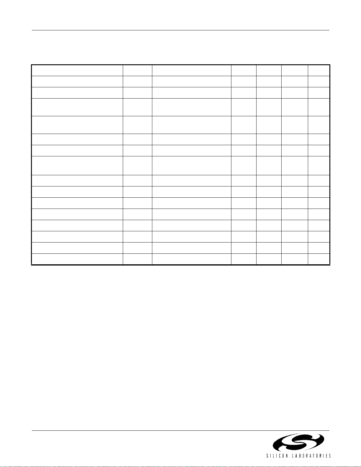
1 1097865432
Si5110
A
B
C
D
E
F
G
RXDIN GND LOSLVL VREF NC RSVD_GND RXCLK[1] RXCLK[1] RXDOUT[1] RXDOUT[0]
RXDIN GND RXLOL LTR RSVD_GND RSVD_GND RXCLK2DSBL RXCLK2DIV RXDOUT[3] RXDOUT[2]
GND LOS RSVD_GND VDD VDD VDD VDD RXMSBSEL RXDOUT[3] RXDOUT[2]
TXCLKOUT GND RESET VDD VDD VDD GND GND GND REFCLK
TXCLKOUT GND REFRATE VDD VDD VDD GND GND GND REFCLK
GND VDD33 RSVD_GND VDD VDD VDD VDD LPTM TXDIN[3] TXDIN[2]
PHASEADJ SLICELVL RXREXT RXSQLCH RSVD_GND RXCLK[2] RXCLK[2] RXDOUT[1] RXDOUT[0]
H
K
TXDOUT GND RSVD_GND TXMSBSEL FIFORST BWSEL DLBK LLBK TXDIN[3] TXDIN[2]
TXDOUT
J
GND NC TXREXT TXLOL TXCLKOUT TXCLKOUT TXCLKIN TXCLKIN TXDIN[1] TXDIN[0]
GND RSVD_GND RSVD_GND FIFOERR TXSQLCH REFSEL TXCLKDSBL TXDIN[1] TXDIN[0]
Top View
Figure 6. Si5110 Pin Configuration (Transparent Top View)
Preliminary Rev. 0.41 17
Page 18

Si5110
Pin Descr i p tio ns : Si 5110
Pin
Number(s)
H6 BWSEL I LVTTL
H7 DLBK
J5 FIFOERR O LVTTL
H5 FIFORST I LVTTL
B2, C2, D1,
E2, E7–9,
F2, F7–9,
G1, H2, J2,
K1
Name I/O Signal Level
ILVTTL
GND GND
Description
Bandw idth Se lec t D S P LL.
This input selects loop bandwidth of the DSPLL.
BWSEL = 0: Loop bandwidth set to 6 kHz.
BWSEL = 1: Loop bandwidth set to 25 kHz.
Diagno s t ic Lo opback.
When this input is active low the transm it clock and
data are looped back for output on RXDOUT , RXCLK1
and RXCLK2. This pin should be held high for normal
operation.
FIFO Error.
This output is driven high when a FIFO overflow/underflow has occurred. This output will stick high
until reset by asserting FIFORST.
FIFO RESET.
This input when asserted high resets the read/write
FIFO pointers to their init ial s tate .
Supply Ground.
H8 LLBK ILVTTL
D2 LOS
B3 LOSLVL I
OLVTTL
Line Loopback.
When this input is active low the recovered clock and
data are looped back for output on TXDOUT, and
TXCLKOUT. This pin should be held high for normal
operation.
Loss-of-Signal.
This output is driven low when the peak-to-peak signal
amplitude is below threshold set via LOSLV L.
LOS Threshold Level.
Applying an analog voltage to this pin allows adjustment of the Threshold used to declar e LOS. Tieing
this input high disables LOS detect ion and fo rces the
LOS
output high.
18 Preliminary Rev. 0.41
Page 19

Si5110
Pin
Number(s)
G8 LPTM I LVTTL
C4 LTR
B5 NC
K2 NC
A2 PHASEADJ I
Name I/O Signal Level
ILVTTL
Description
Loop Timed Opera tion.
When this input is forced high , the recover ed c lock
from the receiver is divided down and us ed as the reference source for the transmit CMU. The narrowband
setting for the DSPLL CMU will be sufficient to provide
SONET compliant jitter generation and transfer on the
transmit data and clock outputs (TXDOUT , TXCLKOUT). This pin should be held low for normal operation.
Lock-to-Reference.
This input forces a stable output clock by locking
RXCLK1 and RXCLK2 to the provided reference.
Driv in g LTR
No Connect.
Reserved for device testing. Leave electrically
unconnected.
No Connect.
Reserved for device testing. Leave electrically unconnected.
Sampling Phase Adjust.
Applying an analog voltage to this pin allows adjustment of the sampling phase acro ss the data eye. Tieing this input high nomina lly cen ters the sampling
phase.
low activates this feature.
E10, F10 REFCLK,
REFCLK
F3 REFRATE I LVTTL
J7 REFSEL I LVTTL
I LVPECL
Differential Reference Clock.
The reference clock sets the operating frequency of
the PLL used to generate the high speed transm it
clock. In addition, REFCLK se ts the initial operat ing
frequency used by the onboard PLL for clock and data
recovery. The Si5110 will operate with reference clock
frequencies that are either 1/16 or 1/32 the serial data
rate (nominally 155 MHz or 78 MHz).
Reference Clock Select.
This input configures the Si5110 to operate with one of
two reference clock frequ enc ies. If REFRATE is held
high, the device requires a reference clock that is 1/16
the serial data rate. If REFRATE is low, a referenc e
clock at 1/32 the serial data rate is required.
Reference Clock Selection.
This inputs selects the reference clock source used by
the CMU. When REFSEL = 0, the low speed data
input clock, TXCLK4IN, is used as the CMU reference. When REFSEL = 0, the reference c lock provided on REFCLK is used.
Preliminary Rev. 0.41 19
Page 20

Si5110
Pin
Number(s)
E3 RESET ILVTTL
A6, B6, C5–
6, D3, G3,
H3, J3–4
B7–8 RXCLK1
C8 RXCLK2DIV I LVTTL
C7 RXCLK2DSBL I LVTTL
Name I/O Signal Level
RSVD_GND
,
RXCLK1
OLVDS
Description
Device Reset.
Forcing this input low for at least 1 µs will cause a
device reset. For normal operation, this pin should be
held high.
Reserved Tie To Ground.
Must tie directly to GND for proper operat ion.
Differential Clock Output 1.
The clock recovered from the sign al pres ent on
RXDIN is divided down to the parallel output word rate
and output on RXCLK1. In the absence of data, a stable clock on RXCLK1 can be maintained by asserting
LTR
.
Clock Divider Select.
This input selects the divide factor us ed to generat e
the RXCLK2 output. When this input is driv en low,
RXCLK2 is equal to the output word rate on RXDOUT.
When driven high, RXCLK2 is 1/4th the outp ut word
rate.
RXCLK2 Disable.
Driving this input high will disable the RXCLK2 output.
This would be used to save power in applications that
do not require an auxiliar y clock.
A7–8 RXCLK2
RXCLK2
B1, C1 RXDIN,
RXDIN
A9–10, B9,
B10, C9,
C10, D9,
D10
C3 RXLOL
RXDOUT[3:0],
RXDOUT
,
[3:0]
OLVDS
I High Speed
Differential
OLVDS
OLVTTL
Differential Clock Output 2.
An auxiliary output clock is provided on this pin that is
equivalent to, or a submultiple of, the output word rate.
The divide factor used in generating RX CLK 2 is set
via RXCLK2DIV.
Differential Data Input.
Clock and data are recovered from the high speed
data signal present on these pins.
Differential Parallel Data Output.
The data recovered from the signal present on RXDIN
is demultiplexed and output as a 4-bit parallel word on
RXDOUT[3:0]. These outputs are updated on the rising edge of RXCLK1.
Loss-of-Lock.
This output is driven low when the recovered clock frequency deviates from the referenc e cloc k by the
amount specified in Table 5.
20 Preliminary Rev. 0.41
Page 21

Si5110
Pin
Number(s)
D8 RXMSBSEL I LVTTL
A4 RXREXT
A5 RXSQLCH
A3 SLICELVL I
Name I/O Signal Level
ILVTTL
Description
Data Bus Receive Order.
This determines the order of the received data bits on
the output bus.
For RXMSBSEL = 0, the first data bit received is output on RXDOUT[0] and following data bits are output
on RDOUT[1] through RXDOUT[3].
For RXMSBSEL = 1, the first data bit is output on
RXDOUT[3] and following data bits are output on
RXDOUT[2] through RXDOUT[0].
External Bias Resistor.
This resistor is used by the receiver c irc uit r y to establish bias currents within the device . This pin must be
connected to GND through a 3.09 k
Data Squelch.
When this input is low the data on RXDOUT is forced
to 0. Set high for normal operation.
Slicing Level Adjustment.
Applying an analog voltage to this pin allows adjustment of the slicing level applied to t he input data eye.
Tieing this input high nominally s ets the slicing offset
to 0.
Ω (1%) resistor.
K7–8 TXCLK4IN
TXCLK4IN
K5–6 TXCLK4OUT
TXCLK4OUT
J8 TXCLKDSBL I LVTTL
E1, F1 TXCLKOUT
TXCLKOUT
,
,
,
ILVDS
OLVDS
Differential Data Clock Input.
The rising edge of this input clocks data present on
TXDIN into the device.
Divided Down Output Clock.
This clock output is generated by dividi ng down the
high speed output clock, TXCLKOUT, by a factor of 4.
It is intended for use in counter clocking schemes that
transfer data between the system ASIC and the
Si5110.
High Speed Clock Disable.
When this input is high, the output drive r for TXCLKOUT is disabled. In applications that do not require the
output data clock, the output clock driver s hould be
disabled to save power.
High Speed Clock Output.
The high speed clock output, TXCLK OUT, is generated by the PLL in the clock multiplier unit . I ts frequency is nominally 16 times or 32 times the selected
reference source.
Preliminary Rev. 0.41 21
Page 22

Si5110
Pin
Number(s)
G9–10, H9–
10, J9–10,
K9–10
H1, J1 TXDOUT,
K4 TXLOL
H4 TXMSBSEL I LVTTL
K3 TXREXT
Name I/O Signal Level
TXDIN[3:0],
TXDIN
[3:0]
TXDOUT
ILVDS
OCML
OLVTTL
Description
Differential Parallel Data Input.
The 4-bit data word present on these pins is multiplexed into a high speed serial stream and output on
TXDOUT. The data on these inputs is clocked into the
device by the rising edge of TXCLK4IN.
Differential High Speed Data Output.
The 4-bit word input on TXDIN[3:0] is multiplexed into
a high speed serial stream that is output on these
pins. Input data is multiplexed in s equence from
TXDIN0 to TXDIN3 with TXDIN0 transmitted first. This
output is updated by the rising edge of TXCLKOUT.
CMU Loss-of-Lock.
The output is asserted low when the CMU is not
phase locked to the selected reference source.
Data Bus Transmit Order.
For TXMSBSEL = 0, data on TXDIN[0] is transmitt ed
first followed by TXDIN[1] through TXDIN[3].
For TXMSBSEL = 1, TXDIN[3] is trans mi tted fi rst fo l lowed by TXDIN[2] through TXDIN[0].
External Bias Resistor.
This resistor is used by the trans m itter ci rcui try to
establish bias currents within the device. This pin must
be connected to GND through a 3.09 k
Ω (1%) resistor.
J6 TXSQLCH
D4–7, E4–6,
F4–6, G4–7
G2 VDD33 VDD33 1.8 V or 3.3 V
B4 VRE F O Voltage Ref
VDD VDD 1.8 V
ILVTTL
Transmit Data Squelch.
If TXSQLCH is asserted low, the output data stream
on TXDOUT will be forced to 0s. If TXSQLCH
squelching is turned off.
Supply Voltage.
Nominally 1.8 V.
Digi ta l O utpu t Su pply.
Must be tied to either 1.8 V or 3.3 V. When tied to
3.3 V, LVTTL compatible output voltage swings on
RXLOL
Voltage Reference.
The Si5110 provides an output voltage reference that
can be used by an external circuit to set the LOS
threshold, slicing level, or sampling phase adjustment.
The equivalent resistance between this pin and GND
should not be less than 10 k
is nominally 1.25 V.
, LOS, TXLOL, and FIFOERR are supported.
Ω. The reference voltage
=1, TX
22 Preliminary Rev. 0.41
Page 23

Ordering Guide
Si5110
Table 9. Ordering Guide
Part Number Package Temperature
Si5110-BC 99 BGA –40°C to 85°C
Preliminary Rev. 0.41 23
Page 24

Si5110
A
Package Ou tlin e
Figure 7 illustrates the package details for the Si5110. Table 10 lists the values for the dimensi ons shown in the
illustration.
1 Ball P ad
Corner
A1 Ball Pad
Corner
D
A
A1
E
b
A2
Seating
Plane
10987654321
e
1.00 Ref
1.00 Ref
A
B
C
D
E
F
G
H
J
K
e
Bottom ViewTop View Side Vi ew
Figure 7. 99-Ball Grid Array (B GA)
Table 10. Package Diagram Dimensions
Symbol Millimeters
Min Nom Max
A 1.30 1.40 1.50
A1 0.31 0.36 0.41
24 Preliminary Rev. 0.41
A2 0.65 0.70 0.75
b — 0.46 —
D—11.00—
E—11.00—
e — 1.00 —
Page 25

NOTES:
Si5110
Preliminary Rev. 0.41 25
Page 26

Si5110
Contact Information
Silicon Laboratori es Inc.
4635 Boston Lane
Austin, TX 78735
Tel: 1+(512) 416-8500
Fax: 1+(512) 416-9669
Toll Free: 1+(877) 444-3032
Email: productinfo @ silabs.com
Internet : w ww.silabs .com
The information in this document is believed to be accurate in all respects at the time of publication but is subject to change withou t notice.
Silico n Laboratories assum es no responsibili ty for errors and omissions, and disclaim s r esponsibility for any conseq uences resulting from
the use of in form ation inclu ded her ein. Addit ionall y, Si licon Labor atories assu mes no re sponsib ility for the fu nction ing of undes cribed fea tures
or parameters. Silicon Laboratories reserves the right to make changes without further notice. Silicon Laboratories makes no warranty, represent ation or gu ara ntee rega rding the suit abilit y of its pro duct s for any particul ar purp ose, nor does Silicon Lab orat ories as sume an y liabili ty
arisin g out of the ap plic at ion or use of any prod uct or circ uit , and sp eci fic ally dis clai ms an y and al l liab i lity , incl udi ng without limitation consequential or incidental damages. Silicon Laboratories products are not designed, intended, or authorized for use in applications intended to
support or sustain life , or for any other application in w hich th e failure of the Silicon L aboratories product could creat e a situation where personal inj ury or death may occur . Should Buyer purchase or use Silicon Laboratories products for any such unintended or unauthorized application, Buyer shall indemnify and hold Silicon Laboratories harmless against all claims and damages.
Silico n Laboratories, Silicon Labs, SiPHY, and DSPL L are trademarks of Silicon Laboratories Inc.
Other products or brandnames mentioned herein are trademarks or registered trademarks of their respective holders.
26 Preliminary Rev. 0.41
 Loading...