

Page 1
Si5022/Si5023
L
P
RELIMINARY DATA SHEET
ULTI-RATE
M
SONET/SDH CDR IC
WITH LIMITING AMP
Features
igh Speed Clock and Data Recovery device with Integrated Limiting Amp:
H
! Supports OC-48/12/3, STM-16/4/1,
Gigabit Ethernet, and 2.7 Gbps FEC
! DSPLL™ Technology
Low Power—370 mW (TYP)
!
! Small Footprint: 5 mm x 5 mm
! Bit-Error-Rate Alarm
! External Reference Not Required
!
Jitter Generation 3.0 mUI
RMS
(TYP)
! Loss-of-signal Level Alarm
! Data Slicing Level Control
! 10 mV
Differential Sensitivity
PP
! 2.5 V (Si5022) or 3.3 V (Si5023) Supply
Applications
! SONET/SDH/ATM Routers
! Add/Drop Multiplexers
! Digital Cross Connects
! Gigabit Ethernet Interfaces
! SONET/SDH Test Equipment
! Optical Transceiver Modules
! SONET/SDH Regenerators
! Board Level Serial Links
Description
The Si5022/23 is a fully integrated, high performance limiting amp and clock and
data recovery (CDR) IC for high-speed serial communication systems. It extracts
timing information and data from a serial input at OC-48/12/3, STM-16/4/1, or
Gigabit Ethernet (GbE) rates. Support for 2.7 Gbps data streams is also provided
for OC-48/STM-16 applications that employ forward error correction (FEC). An
external reference clock is not required; applications with or without an external
reference clock are supported. Silicon Laboratories’ DSPLL
™
technology
eliminates sensitive noise entry points thus making the PLL less susceptible to
board-level interaction and helping to ensure optimal jitter performance.
The Si5022/23 represents a new standard in low jitter, low power, small size, and
integration for high speed LA/CDRs. It operates from either a 3.3 V (Si5023) or
2.5 V (Si5022) supply over the industrial temperature range (–40°C to 85°C).
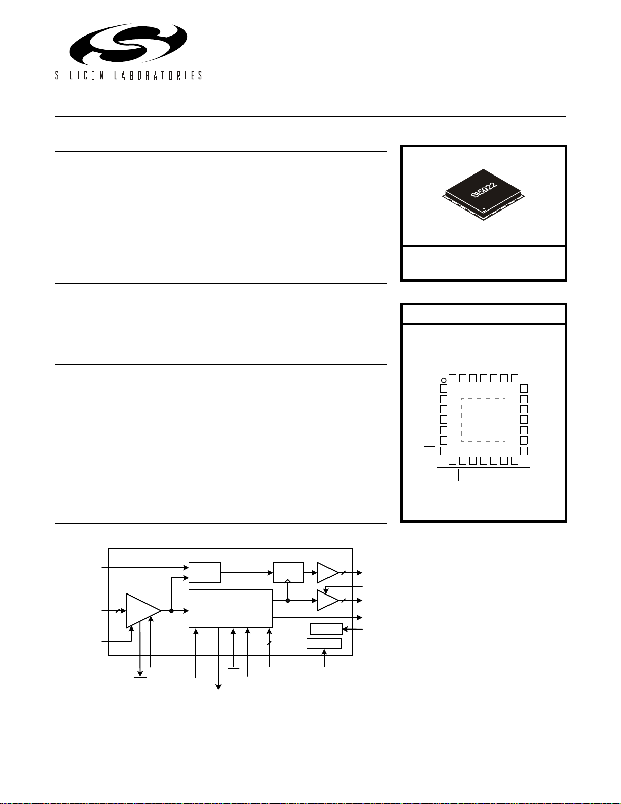
Functional Block Diagram
Ordering Information:
See page 14.
Pin Assignments
Si5022/23
NC
BER_ALM
RATESEL0
RATESEL1
LOS_LVL
SLICE_LVL
REFCLK+
REFCLK–
LOL
1
2
3
4
5
6
7
LTR
LOS
Top View
BER_LVL
GND
Pad
DSQLCH
VDD
VDD
CLKDSBL
DIN+
CLKOUT+
DIN–
22232425262728
141312111098
CLKOUT–
21
20
19
18
17
16
15
VDD
VDD
REXT
RESET/CA
VDD
DOUT+
DOUT–
TDI
DSQLCH
DIN+
DIN–
LOS_LVL
2
Limiting
AMP
LOS
SLICE_LVL
Squelch
Control
BER_LVL
DSPLL
Phase-Locked
Loop
BER_ALM
TM
LTR
REFCLK+
REFCLK–
(Optional)
Retimer
2
RATSEL[1:0]
BUF
BUF
Control
Bias Gen
REXT
2
2
DOUT+
DOUT–
CLKDSBL
CLKOUT+
CLKOUT–
LOL
RESET/CAL
Preliminary Rev. 0.46 5/01 Copyright © 2001 by Silicon Laboratories Si5022/23-DS046
This information applies to a product under development. Its characteristics and specifications are subject to change without notice.
Silicon Laboratories Confidential. Information contained herein is covered under non-disclosure agreement (NDA).
Page 2

Si5022/Si5023
2 Preliminary Rev. 0.46
Page 3

Si5022/Si5023
T
ABLE OF
C
ONTENTS
Section Page
Detailed Block Diagram . . . . . . . . . . . . . . . . . . . . . . . . . . . . . . . . . . . . . . . . . . . . . . . . . . 4
Electrical Specifications . . . . . . . . . . . . . . . . . . . . . . . . . . . . . . . . . . . . . . . . . . . . . . . . . 5
Functional Description . . . . . . . . . . . . . . . . . . . . . . . . . . . . . . . . . . . . . . . . . . . . . . . . . . 11
Limiting Amplifier . . . . . . . . . . . . . . . . . . . . . . . . . . . . . . . . . . . . . . . . . . . . . . . . . . . . 11
DSPLL™ . . . . . . . . . . . . . . . . . . . . . . . . . . . . . . . . . . . . . . . . . . . . . . . . . . . . . . . . . . 11
Multi-Rate Operation . . . . . . . . . . . . . . . . . . . . . . . . . . . . . . . . . . . . . . . . . . . . . . . . . 11
Operation Without an External Reference . . . . . . . . . . . . . . . . . . . . . . . . . . . . . . . . . 11
Operation With an External Reference . . . . . . . . . . . . . . . . . . . . . . . . . . . . . . . . . . . 12
Lock Detect . . . . . . . . . . . . . . . . . . . . . . . . . . . . . . . . . . . . . . . . . . . . . . . . . . . . . . . . 12
Lock-to-Reference . . . . . . . . . . . . . . . . . . . . . . . . . . . . . . . . . . . . . . . . . . . . . . . . . . . 12
Loss-of-Signal . . . . . . . . . . . . . . . . . . . . . . . . . . . . . . . . . . . . . . . . . . . . . . . . . . . . . . 12
Bit-Error-Rate (BER) Detection . . . . . . . . . . . . . . . . . . . . . . . . . . . . . . . . . . . . . . . . . 13
Data Slicing Level . . . . . . . . . . . . . . . . . . . . . . . . . . . . . . . . . . . . . . . . . . . . . . . . . . . 13
PLL Performance . . . . . . . . . . . . . . . . . . . . . . . . . . . . . . . . . . . . . . . . . . . . . . . . . . . . 13
RESET/DSPLL Calibration . . . . . . . . . . . . . . . . . . . . . . . . . . . . . . . . . . . . . . . . . . . . . 14
Clock Disable . . . . . . . . . . . . . . . . . . . . . . . . . . . . . . . . . . . . . . . . . . . . . . . . . . . . . . . 14
Data Squelch . . . . . . . . . . . . . . . . . . . . . . . . . . . . . . . . . . . . . . . . . . . . . . . . . . . . . . . 14
Device Grounding . . . . . . . . . . . . . . . . . . . . . . . . . . . . . . . . . . . . . . . . . . . . . . . . . . . 14
Bias Generation Circuitry . . . . . . . . . . . . . . . . . . . . . . . . . . . . . . . . . . . . . . . . . . . . . . 14
Voltage Regulator . . . . . . . . . . . . . . . . . . . . . . . . . . . . . . . . . . . . . . . . . . . . . . . . . . . 14
Differential Input Circuitry . . . . . . . . . . . . . . . . . . . . . . . . . . . . . . . . . . . . . . . . . . . . . . 14
Differential Output Circuitry . . . . . . . . . . . . . . . . . . . . . . . . . . . . . . . . . . . . . . . . . . . . 16
Pin Descriptions: Si5022/23 . . . . . . . . . . . . . . . . . . . . . . . . . . . . . . . . . . . . . . . . . . . . . . 17
Ordering Guide . . . . . . . . . . . . . . . . . . . . . . . . . . . . . . . . . . . . . . . . . . . . . . . . . . . . . . . . . 20
Package Outline . . . . . . . . . . . . . . . . . . . . . . . . . . . . . . . . . . . . . . . . . . . . . . . . . . . . . . . . 21
Contact Information . . . . . . . . . . . . . . . . . . . . . . . . . . . . . . . . . . . . . . . . . . . . . . . . . . . . . 22
Preliminary Rev. 0.46 3
Page 4
Si5022/Si5023
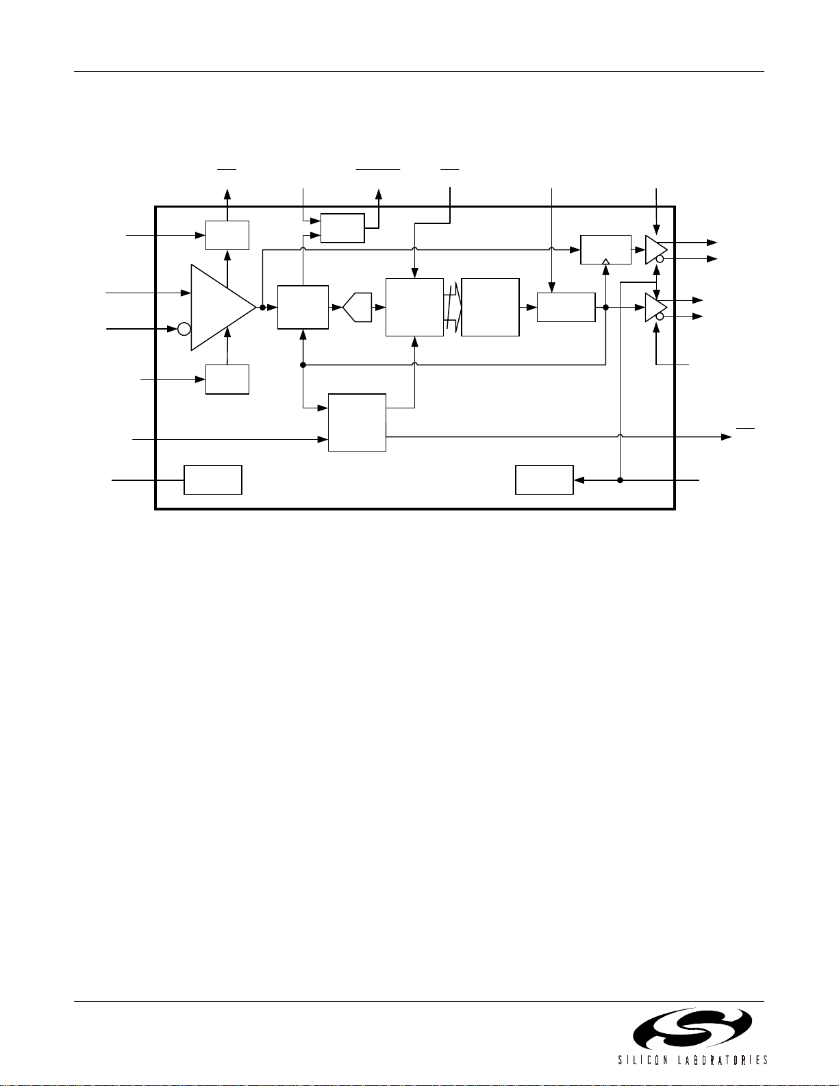
Detailed Block Diagram
LOS_LVL
DIN+
DIN+
SLICE_LVL
REFCLK±
(optional)
REXT
Signal
Detect
Limiting
Amp
Slicing
Control
Bias
Generation
LTR
DSP VCO
n
Phase
Detector
BER_ALMBER_LVLLOS
BER
Monitor
A/D
Lock
Detection
Figure 1. Detailed Block Diagram
RATESEL[0:1]
Retime
CLK
Dividers
Calibration RESET/CAL
DSQLCH
DOUT+
DOUT–
CLKOUT+
CLKOUT–
CLK_DSBL
LOL
4 Preliminary Rev. 0.46
Page 5
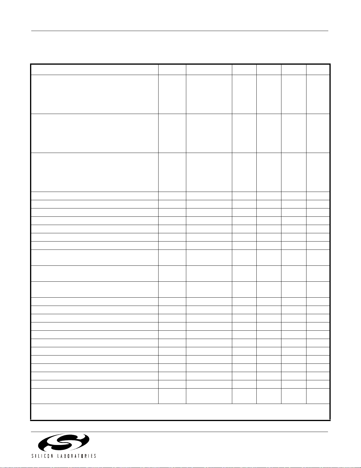
Electrical Specifications
Table 1. Recommended Operating Conditions
Si5022/Si5023
Parameter
Symbol Test Condition
Ambient Temperature T
Si5022 Supply Voltage
Si5023 Supply Voltage
2
2
V
V
A
DD
DD
1
Min
Typ
–40 25 85 °C
2.375 2.5 2.625 V
3.135 3.3 3.465 V
Max
1
Notes:
1. All minimum and maximum specifications are guaranteed and apply across the recommended operating
conditions. Typical values apply at nominal supply voltages and an operating temperature of 25°C unless
otherwise stated.
2. The Si5022/23 specifications are guaranteed when using the recommended application circuit (including
component tolerance) of Figure 5 on page 10.
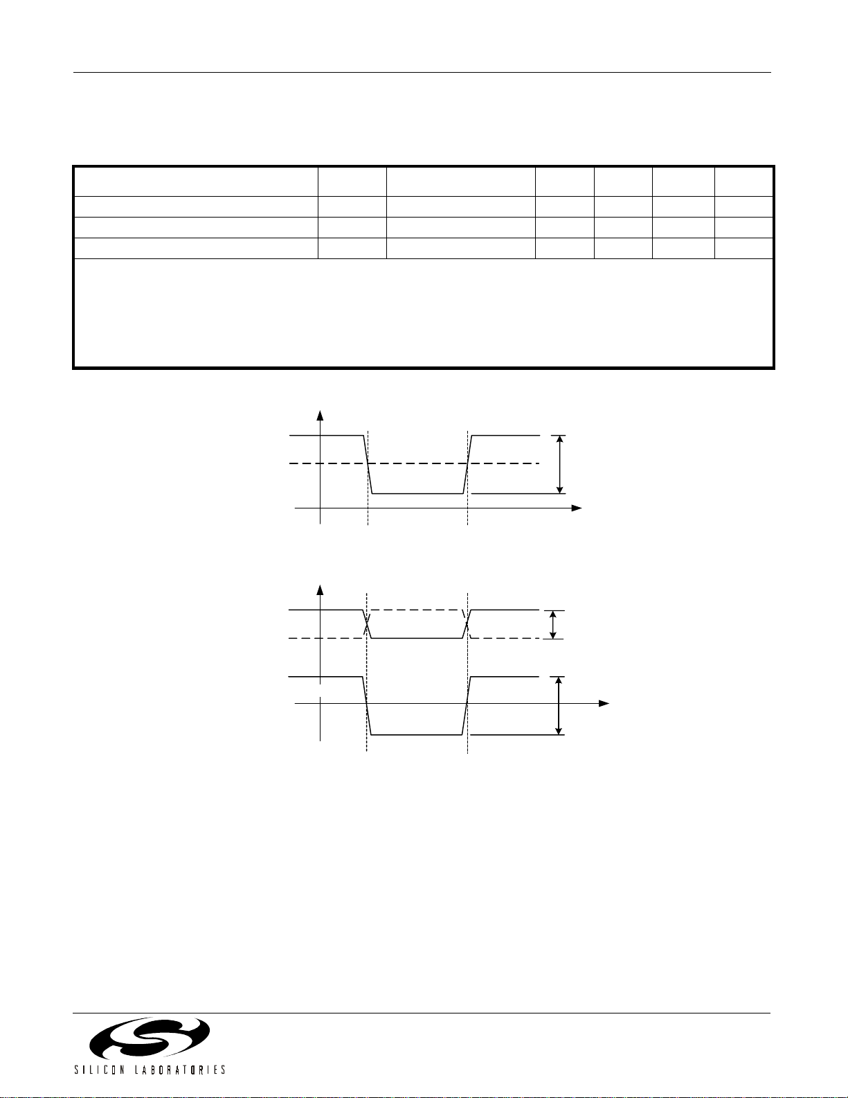
V
SIGNAL+
SIGNAL–
A. Operation with Single-Ended Inputs
V
IS
t
Unit
V
SIGNAL+
0.5 V
SIGNAL–
(SIGN A L +) – (SIG N A L –)
B. Operation with Differential Inputs and Outputs
ID
V
ID
t
Figure 2. Differential Voltage Measurement (DI N , REFCLK, DOUT, CLKOUT)
Preliminary Rev. 0.46 5
Page 6
Si5022/Si5023
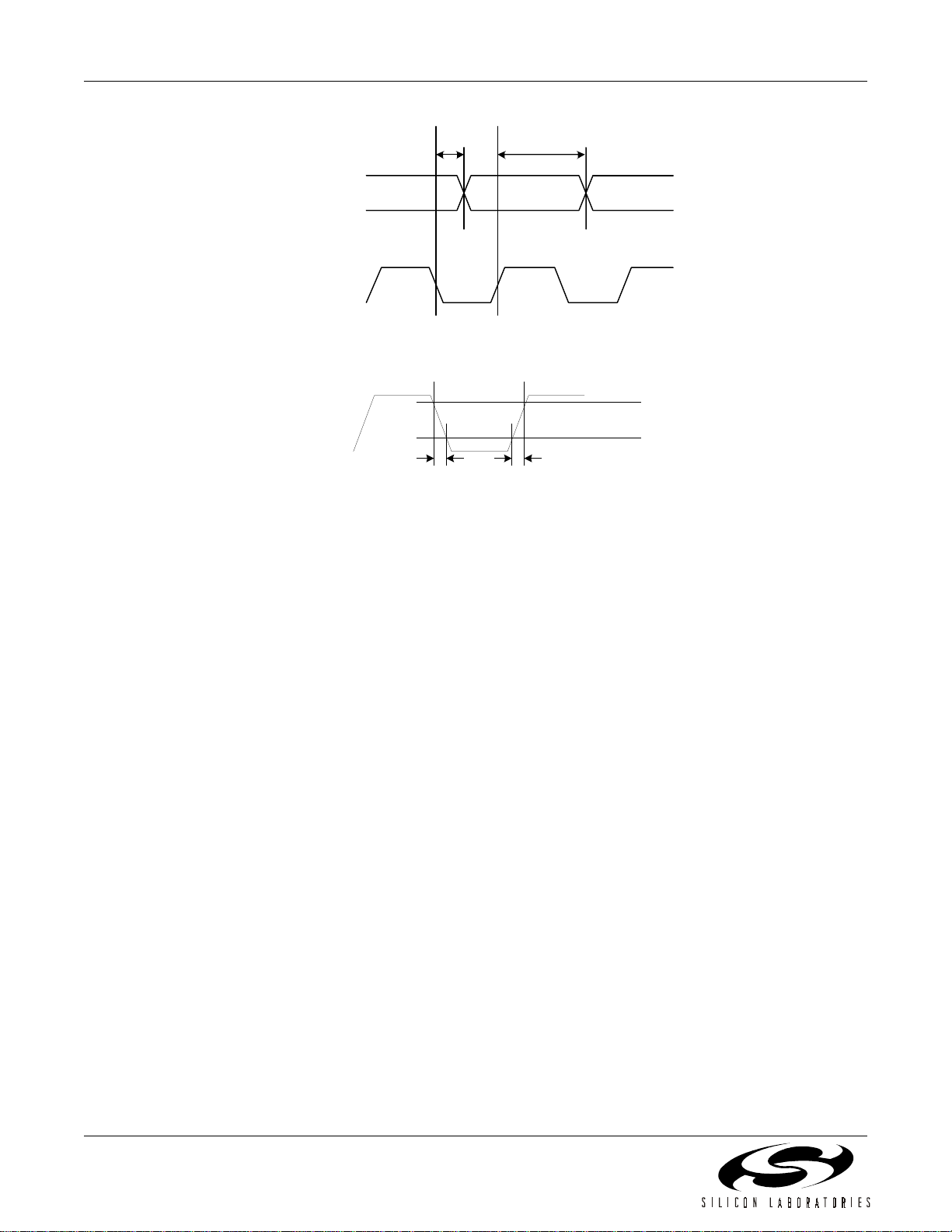
t
Cr-D
DOUT
CLKO UT
t
Cf-D
Figure 3. Clock to Data Timing
DOUT,
CLKOUT
t
F
t
R
Figure 4. DOUT and CLKOUT Rise/Fall Times
80%
20%
6 Preliminary Rev. 0.46
Page 7
Si5022/Si5023
Table 2. DC Characteristics
(VDD=2.5 V ± 5% for Si5022 or 3.3V ± 5% for Si5023, TA = –40°C to 85°C)
Parameter Symbol Test Condition Min Typ Max Unit
Supply Current
OC-48 and FEC (2.7 G Hz)
GigE
OC-12
OC-3
Power Dissipation
OC-48 and FEC (2.7 G Hz)
GigE
OC-12
OC-3
Power Dissipation
OC-48 and FEC (2.7 G Hz)
GigE
OC-12
OC-3
Common Mode Input Voltage (DIN)* V
Common Mode Input Voltage (REFCLK)* V
DIN Single-ended Input Voltage Swing* V
DIN Differential Input Voltage Swing* V
REFCLK Single-ended Input Voltage Swing* V
REFCLK Differential Input Voltage Swing* V
Input Impedance (DIN, REFCLK) R
Differential Output Voltage Swing
(DOUT)
Differential Output Voltage Swing
(CLKOUT)
Output Common Mode Voltage
(DOUT,CLKOUT)
Output Impedance (DOUT,CLKOUT) R
Output Current Short to GND (DOUT,CLKOUT) I
Output Current Short to V
(DOUT,CLKOUT) I
DD
Input Voltage Low (LVTTL Inputs) V
Input Voltage High (LVTTL Inputs) V
Input Low Current (LVTTL Inputs) I
Input High Current (LVTTL Inputs) I
Output Voltage Low (LVTTL Outputs) V
Output Voltage High (LVTTL Outputs) V
Input Impedance (LVTTL Inputs) R
PWRDN/CAL Leakage Current I
LOS_LVL, BER_LVL, SLICE_LVL Input Imped-
ance
*Note: These inputs may be driven differentially or single-endedly. When driven single-endedly, the unused input must be ac
coupled to ground.
I
DD
P
D
VDD =
2.5 V (
P
D
VDD =
3.3 V (
See Figure 11 1.42 1.50 1.58 V
See Figure10 1.90 2.00 2.10 V
See Figure 2A 10 — 500 mV
See Figure 2B 10 — 1000 mV
See Figure 2A 200 — 750 mV
See Figure 2B 200 — 1500 mV
Line-to-Line 84 100 116 Ω
100 Ω Load
V
ICM
ICM
IS
ID
IS
ID
IN
OD
Line-to-Line
V
OD
100 Ω Load
Line-to-Line
V
OCM
100 Ω Load
Line-to-Line
OUT
SC(–)
SC(+)
IL
IH
IL
IH
OL
OH
IN
PWRDNVPWRDN
R
IN
Single-ended 84 100 116 Ω
IO = 2 mA — — 0.4 V
IO = 2 mA 2.0 — — V
± 5%)
± 5%)
—
—
—
—
—
—
—
—
—
—
—
—
148
150
152
154
370
375
380
385
488
495
502
508
160
162
164
165
400
405
410
414
554
561
568
572
mA
mW
mW
TBD 940 TBD mV
(pk-pk)
TBD 900 TBD mV
(pk-pk)
TBD 1.825 TBD V
—25TBDmA
TBD –15 — mA
——.8V
2.0 — — V
——10µA
——10µA
10 — — kΩ
≥ 0.8 V TBD 25 TBD µA
TBD 100 TBD kΩ
Preliminary Rev. 0.46 7
Page 8

Si5022/Si5023
Table 3. AC Characteristics (Clock and Data)
(VDD=2.5 V ± 5% for Si5022 or 3.3V ± 5% for Si5023, TA = –40°C to 85°C)
Parameter Symbol Test Condition Min Typ Max Unit
Output Clock Rate f
Output Rise Time t
Output Fall Time t
Clock to Data Delay
CLK
t
Cr-D
R
F
Figure 4 — 100 TBD ps
Figure 4 — 100 TBD ps
Figure 3
FEC (2.7 GHz)
OC-48
GigE
OC-12
OC-3
Clock to Data Delay
t
Cf-D
Figure 3
FEC (2.7 GHz)
OC-48
Input Return Loss 100 kHz–2.5 GHz
2.5 GHz–4.0 GHz
Slicing Level Offset*
(relative to the internally set input
common mode voltage)
V
SLICE
SLICE_LVL = 750 mV to
2.25 V
Slicing Level Accuracy SLICE_LVL = 750 mV to
.15 — 2.7 GHz
TBD
TBD
TBD
TBD
TBD
TBD
TBD
TBD
TBD
250
255
500
890
4100
TBD
TBD
—
—
–15 — 15 mV
–500 — 500 µV
2.25 V
*Note: Adjustment voltage (relative to the internally set input common mode voltage) is calculated as follows:
(SLICE_LVL – 1.50 V)/50.
TBD
TBD
TBD
TBD
TBD
TBD
TBD
—
—
V
SLICE
ps
ps
dB
dB
=
8 Preliminary Rev. 0.46
Page 9

Si5022/Si5023
Table 4. AC Characteristics (PLL Characteristics)
(VDD=2.5 V ± 5% for Si5022 or 3.3V ± 5% for Si5023, TA = –40°C to 85°C)
Parameter Symbol Test Condition Min Typ Max Unit
Jitter Tolerance
J
TOL(PP)
(OC-48)*
Jitter Tolerance
(OC-12 Mode)
*
Jitter Tolerance
(OC-3 Mode)
*
Jitter Tolerance (Gigabit Ethernet)
J
TOL(PP)
J
TOL(PP)
T
JT(PP)
IEEE 802.3z Clause 38.68 600 TBD — ps
Receive Data Total Jitter
Tolerance
Jitter Tolerance (Gigabit Ethernet)
D
JT(PP)
IEEE 802.3z Clause 38.69 370 TBD — ps
Receive Data Deterministic Jitter
Tolerance
RMS Jitter Generation
*
Peak-to-Peak Jitter Generation
Jitter Transfer Bandwidth
Jitter Transfer Peaking
*
*
Acquisition Time
*
J
GEN(RMS)
J
GEN(PP)
J
BW
J
P
T
AQ
with no jitter on serial data — 3.0 5.0 mUI
with no jitter on serial data — 25 55 mUI
(Reference clock applied)
Acquisition Time
T
AQ
(Reference-less operation)
Reference Clock Range 19.44 — 168.75 MHz
Input Reference Clock Frequency
C
TOL
Tolerance
Frequency Difference at which
Receive PLL goes out of Lock
(REFCLK compared to the divided
down VCO clock)
Frequency Difference at which
Receive PLL goes into Lock (REFCLK compared to the divided
down VCO clock)
*Note: As defined in Bellcore specifications: GR-253-CORE, Issue 2, December 1995. Using PRBS 223– 1 data pattern.
f = 600 Hz 40 TBD — UI
f = 6000 Hz 4 TBD — UI
f = 100 kHz 4 TBD — UI
f = 1 MHz 0.4 TBD — UI
f = 30 Hz 40 TBD — UI
f = 300 Hz 4 TBD — UI
f = 25 kHz 4 TBD — UI
f = 250 kHz 0.4 TBD — UI
f = 30 Hz 60 TBD — UI
f = 300 Hz 6 TBD — UI
f = 6.5 kHz 6 TBD — UI
f = 65 kHz 0.6 TBD — UI
OC-48 Mode — — 2.0 MHz
OC-12 Mode — — 500 kHz
OC-3 Mode — — 130 kHz
— 0.03 0.1 dB
After falling edge of
1.45 1.5 1.7 ms
PWRDN/CAL
From the return of valid
40 60 150 µs
data
After falling edge of
TBD TBD TBD ms
PWRDN/CAL
From the return of valid
TBD TBD TBD ms
data
–100 — 100 ppm
TBD 600 TBD ppm
TBD 300 TBD ppm
PP
PP
PP
PP
PP
PP
PP
PP
PP
PP
PP
PP
Preliminary Rev. 0.46 9
Page 10

Si5022/Si5023
Table 5. Absolute Maximum Ratings
Parameter Symbol Value Unit
DC Supply Voltage V
DD
–0.5 to 2.8 (Si5022)
V
–0.5 to 3.5 (Si5023)
LVTTL Input Voltage V
Differential Input Voltages V
DIG
DIF
–0.3 to 3.6 V
–0.3 to (VDD+ 0.3) V
Maximum Current any output PIN ±50 mA
Operating Junction Temperature T
Storage Temperature Range T
JCT
STG
–55 to 150 °C
–55 to 150 °C
Lead Temperature (soldering 10 seconds) 300 °C
ESD HBM Tolerance (100pf, 1.5 kΩ)1kV
Note: Permanent device damage may occur if the above Absolute Maximum Ratings are exceeded. Functional operation
should be restricted to the conditions as specified in the operational sections of this data sheet. Exposure to absolute
maximum rating conditions for extended periods may affect device reliability.
Table 6. Thermal Characteristics
Parameter Symbol Test Condition Value Unit
Thermal Resistance Junction to Ambient ϕ
LVTTL
Control Inputs
JA
BER Alarm
Indicator
Loss-of-Lock
Still Air 38 °C/W
Loss-of-Signal
Indicator
Indicator
High Speed
Serial Input
System
Reference
Clock
(Optional)
2
LOL
DOUT+
DOUT–
DIN+
DIN–
LTR
CLKDSBL
DSQLCH
RESET/CAL
RATESEL1-0
BER_ALM
Si5022/23
REFCLK+
REFCLK–
LOS_LVL
Loss-of-Signal
Level Set
Bit Error Rate
Level Set
BER_LVL
SLICE_LVL
Data Slice
Level Set
10 k
REXT
VDD
ΩΩΩΩ
CLKOUT+
CLKOUT–
VDD
µµµµ
0.1
F
2200 pF
20 pF
GND
Figure 5. Si5022/23 Typical Application Circuit
LOS
Recovered
Data
Recovered
Clock
10 Preliminary Rev. 0.46
Page 11

Functional Description
Si5022/Si5023
The Si5022/23 integrates a high-speed limiting amplifier
(LA) with a multi-rate clock and data recovery unit
(CDR) that operates up to 2.7 Gbps. No external
reference clock is required for clock and data recovery.
The limiting amplifier magnifies very low-level input data
signals so that accurate clock and data recovery can be
performed. The CDR uses Silicon Labo ratories’ DSPLL
technology to reco ver a clock synch ronous to the input
data stream. The rec overed clock is used to retime th e
incoming data, and both are output synchronously via
current-mode logic (CML) drivers. Silicon Laboratories’
DSPLL technology ensures superior jitter p erformance
while eliminating the need for external loop filter
components found in traditional phase-lock loop
implementations.
The limiting amplifier includes a control input for
adjusting the 0/1 data sl icing leve l and provides a loss of-signal level alarm output. The CDR includes a biterror-rate performa nc e m oni tor w hic h si gn als a h igh biterror-rate condition (associated with excessive
incoming jitter) relative to an externally adjustable biterror-rate threshold.
The optional reference clock minimizes the CDR
acquisition time and provides a stable reference for
maintaining the output clock when locking to reference
is desired.
Limiting Amplifier
The limiting amplifier accepts the low-level signal output
from a transimpedance amplifier (TIA). The low-level
signal is amplified to a usable level for the clock and
data recovery unit. The minimum input swing
requirement is specified in Table 2. Larger input
amplitudes (up to the max imum i nput sw ing spe cifi ed in
Table 2) are accommodated without degradation of
performance. The limiting amplifier ensures optimal
data slicing by using a digital dc offset cancellation
technique to remove any dc bias introduced by the
amplification stage.
DSPLL
The Si5022/23 PLL structure (shown in Figure 1 on
page 4) utilizes Si lico n Labor atories ' DSPL L te chnol ogy
to maintain superior jitter performance while eliminating
the need for external loop filter components found in
traditional PLL implementations. This is achieved by
using a digital signal processing (DSP) algorithm to
replace the loop filter commonly found in analog PLL
designs. This algorithm processes the phase detector
error term and generates a digital control value to adjust
the frequency of th e v ol tage c ont roll ed os ci ll ato r (V CO) .
™
This technology enables clock and data recovery with
far less ji tt er t ha n is ge nerated usin g traditiona l m e tho d s
and it eliminates performance degradation caused by
external component aging. In addition, because
external loop filter components are not required,
sensitive noise en try poin ts ar e elim inated , thus m aking
the DSPLL less susceptible to board-level noise
sources and making SONET/SDH jitter compliance
easier to attain in the application.
Multi-Rate Operation
The Si5022/23 supports clock and data recovery for
OC-48 and STM-16 data stre ams. In addition, the PLL
was designed to operate at data rates up to 2.7 Gbps to
support OC-48/STM-16 applications that employ
forward error correction (FEC).
Multi-rate operation is achieved by configuring the
device to divide down the output of the VCO to the
desired data rate. The divi de factor is confi gured by th e
RATESEL[0:1] pins. The RATESEL[0:1] configuration
and associated data rates are given in Table 7.
Table 7. Multi-Rate Configuration
OC-48
RATESEL
[0:1]
11 2.488 Gbps — 2.67 Gbps 1
10 1.244 Gbps 1.25 Gbps — 2
01 622.08 Mbps — — 4
00 155.52 Mbps — — 16
SONET/
SDH
Gigabit
Ethernet
with
15/14
FEC
CLK
Divider
Operation Without an External Reference
The Si5022/23 can perform clock and data recovery
without an external referen ce clock. Tying the REFCLK
inputs to GND configures the device to operate without
an external reference c lock. Clock recove ry is achie ved
by monitoring the timing quality of the incoming data
relative to the VCO frequency. Lock is maintained by
continuously monitoring the incoming data timing quality
and adjusting the VCO accordingly. Details of the lo ck
detection and the lock-to-reference functions while in
this mode are described in their respective sections
below.
Note: Without an ex t er na l r e fe re nc e t h e a cq u is it i on o f da ta is
dependent solely on the data itself and will typically
require more time to acquire lock than when a reference is applied.
Preliminary Rev. 0.46 11
Page 12

Si5022/Si5023
)
Operation With an External Reference
The Si5022/23 device’s optional external reference
clock centers the DSPLL, minimizes the acquisition
time, and maintains a stable output clock (CLKOUT)
when lock-to-reference (LTR
) is asserted.
When the reference clock is present, the Si502 2/23 will
use the reference clock to center the VCO output
frequency so that clock and data can be recovered from
the input data stream. The de vice will self con figure for
operation with one of thr ee refe re nc e cl ock fr eq uen ci es .
This eliminates the need to externally configure the
device to operate with a particular reference clock.
The reference clock centers the VCO for a nominal
output between 2.5 and 2.7 GHz. The VCO frequency is
centered at 16, 32, or 128 times the reference clock
frequency. Detection circuitry continuously mon itors the
reference clock input to determine whether the devic e
should be configur ed for a reference clock tha t is 1/16,
1/32, or 1/128 the nominal VCO output. Approximate
reference clock frequencies for some target applications
are given in Table 8.
Table 8. Typical REFCLK Frequencies
SONET/
SDH with
15/14 FEC
SONET/SDH
Gigabit
Ethernet
19.44 MHz 19.53 MHz 20.83 MHz 128
77.76 MHz 78.125 MHz 83.31 MHz 32
155.52 MHz 156.25 MHz 166.63 MHz 16
Ratio of
VCO to
REFCLK
Lock Detect
The Si5022/23 provides lock-detect circuitry that
indicates whether the PL L has achieved freque ncy lock
with the incoming data. The operation of the lockdetector depends on the reference clock option used.
When an external reference clock is provided, the circuit
compares the frequency of a divided down version of
the recovered clock wi th the frequency of the supplied
reference clock (REFCLK). If the recovered clock
frequency deviates from that of the re ference clock by
the amount specified in Table 4 on page 9, the PLL is
declared out of lock, and the loss-of-lock (LOL
asserted. In this s tate, the DSPLL will periodica lly tr y to
reacquire lock with the incoming data stream. During
reacquisition, the recov ered clock frequ ency (CLKO UT)
will drift over a 1% range relative to the supplied
reference clock. The LOL
output will remain asserted
until the recovered clock frequency is within the
REFCLK frequency by the amount specified in Table 4
on page 9. In applications requiring a more stable
) pin is
output clock during out-of-lock conditions, the lock-toreference (LTR
) input can be used to force t he PLL to
lock to the externally supplied reference.
In the absence of an external refere nce, the lock detec t
circuitry uses a data quality measure to determine when
frequency lock has been lost with the incoming data
stream. Once LOL
has been asserted, it will remain
active until data is reacquired. During thi s reacquisition
period, CLKOUT may vary by approximately ±10% from
the nominal data rate. For applications req uir i ng a m or e
stable output clock during out-of-lock conditions, LTR
can be used to stabilize the output clock.
Lock-to-Reference
The lock-to-reference input (L TR) can be used to force a
stable output clock when an alarm conditio n, like LOS,
exists. In typica l applications, the LOS
tied to the LTR
input to force a stable output clock when
the input data signal is los t. When LTR
output would be
is asserted, the
DSPLL is prevented from acquiring the data signal
present on DIN. The operati on of the LTR
control inpu t
depends on which reference clocking mode is used.
When an external referenc e clock is present, assertio n
of LTR
will force the DSPLL to lock CLKOUT to the
provided reference. If no external reference clock is
used, LTR
will force the DSPLL to hold the digital
frequency control input to the VCO at the last value.
This produces an outpu t clock that is stable as long as
supply and temperature are constant.
Loss-of-Signal
The Si5022/23 indicates a loss-of-signal condition on
the LOS
level on DIN falls below an externally controlled
threshold. The LOS threshold range is specified in
Table 3 and is set by applying a voltage on the
LOS_LVL pin. The graph in Figure 6 illustrates the
LOS_LVL mapping to the LOS threshold. The LOS
output is asserted when the input signal drops below the
programmed peak-to-peak value.
output pin w hen the input peak-to-peak signal
)
PP
30 mV
15 mV
LOS Disabled
LOS Threshold (mV
0 mV
0 V
LOS
Undefined
LOS_LVL (V
1.875 V
40mV/V
2.25 V1.50 V1.00 V
Figure 6. LOS_LVL Mapping
12 Preliminary Rev. 0.46
Page 13

Si5022/Si5023
Approximately 6 dB of level detection hysteresis
prevents unnecess ary s witching on LOS
when marginal
input data swing peak-to-peak levels are present.
Hysteresis is defined as the difference between the LOS
deassert level (LOSD) and the LOS assert level
(LOSA). The hysteresis in decibels is calculated as
20log((LOSD – LOSA)/LOSA). The relationship
between the LOS
level is shown in Figure 7. When the LOS
assert level and the LOS deassert
assert level is
set below 10 mV, the amount of hysteresis is fixed at
5 mV. When the LOS assert level is set above 10 mV,
the amount of hysteresis is approximately 6 dB.
45 mV
)
PP
(m V
LOS D eassert Level
15 mV
11 mV
common mode voltage) are su pported. The 0/1 slicing
level is set by apply ing a voltage between 0.75 V and
2.25 V to the S LICE_LVL input. The voltage present on
SLICE_LVL maps to the 0/1 slicing level as follows:
where V
V
SLICE_LVL
V
SLICE
is the slicing l evel and V
SLICE
-------------------------------------------------------=
1.5 V–()
50
SLICE_LVL
is the
voltage applied to the SLICE_LVL pin.
When SLICE_LVL is driven below 500 mV, the 0/1
slicing level ad jus tm ent is di sabl ed, and the s li cing lev el
is set to the cross-point of the differential input signal.
PLL Performance
The PLL implementatio n used in the Si5022/23 is fully
compliant with the jitter specifications proposed for
SONET/SDH equipment by Bellcore GR-253-CORE,
Issue 2, December 1995 and ITU-T G.958.
Jitter Tolerance
The Si5022/23’s tolera nce to in put jitter ex ceeds t hat of
the Bellcore/ITU mask shown in Figure 8. This mask
defines the level of peak-to-peak sinusoid jitter that
must be tolerated when applied to the differential data
input of the device.
Note: There are no entries in the mask table for the data rate
corresponding to OC-24 as that rate is not specified by
either GR-253 or G.958.
6 mV
10 mV
30 mV
LOS As sert Level (mVPP)
Figure 7. Hysteresis Dependency
Bit-Error-Rate (BER) Detection
The Si5022/23 uses a proprietary Silicon Laborato ries
algorithm to generate a bit-error-rate (BER) alarm on
the BER_ALM
pin if the observed BER is greater tha n a
user programmable thr eshold. Bit error detec tion relies
on the input data edge timing; edges o ccurring outside
of the expected event wi nd ow ar e co unte d as bit errors.
The BER alarm threshold can be set to one of 64
discrete values between 10
–3
and 10–4. The BER
threshold is programmed by applying a voltage to the
BER_LVL pin between 500 mV and 2.25 V
corresponding to 10
-3
and 10-4 respectively.
Data Slicing Level
The Si5022/23 provides th e ability to externally adjust
the 0/1 slicing level for applications that require biterror-rate (BER) optimization. Adjustments in slicing
level of ±15 mV (relative to the internally set input
Sinusoidal
Input
Jitter (U I
)
PP
15
1.5
0.15
SONET
Data Rate
OC-48
OC-12
OC-3
Slope = 20 dB/Decade
f0 f1 f2 f3 ft
F0
(Hz )F1(Hz )F2(kHz )
10
10
10
Frequency
600
30
30
6000
300
300
F3
(kHz )Ft(kHz )
100 1000
25
6.5
250
65
Figure 8. Jitter Tolerance Specification
Jitter Transfer
The Si5022/23 exceeds all relevant Bellcore/ITU
specifications related to SONET/SDH jitter transfer.
Jitter transfer is defined as the ratio of output signal jitter
to input signal jitter as a function of jitter frequency . (See
Figure 9. ) The se meas ur em ents ar e ma de wi th an input
Preliminary Rev. 0.46 13
Page 14

Si5022/Si5023
test signal that is degraded wi th sinusoidal jitter whose
magnitude is defined by the mask in Figure 9.
Jitter
Transfer
0.1 dB
Acceptable
Range
Fc
Frequency
SONET
Data Rate
OC-48
OC-12
OC-3
20 dB/Decade
Slope
Fc
(kHz )
2000
500
130
Figure 9. Jitter Transfer Specification
Jitter Generation
The Si5022/23 exceeds all relevant specifications for
jitter generation p roposed for SONET/SDH equip ment.
The jitter generation specification defines the amount of
jitter that may be present on the recovered clock and
data outputs when a jitter free input signal is provided.
The Si5022/23 typically generates less than
3.0 mUI
of jitter when presented with jitter-free input
RMS
data.
RESET/DSPLL Calibration
The Si5022/23 achieves optimal jitter performance by
using self-calibration circuitry to set the loop gain
parameters within the DSPLL. For the self-calibration
circuitry to operate correctly, the power supply voltage
must exceed TBD V when calibration occurs. Selfcalibration is initi ated by a high-to-low trans ition on the
RESET/CAL pin. The RESET/CAL pin must be held
high for at least 1 µS after the suppl y has stabilized on
power-up for optimum d evice operation. W hen RESET/
CAL is released (set to low) the digital logic resets to a
known initial conditio n, recali brates the DSP LL, and will
begin to lock to the incoming data stream.
Clock Disable
The Si5022/23 provides a clock disable pin,
CLK_DSBL, that is used to disable the recovered clock
output, CLKOUT. When the CLK_DSBL pin i s asserted ,
the positive and negativ e terminals of CLK OUT are tied
to VDD through 100 Ω on-chip r esistors. Thi s feature is
used to reduce power consum ption in applications that
do not use the recovered clock.
Data Squelch
The Si5022/23 provides a data squelching pin,
DSQLCH, that is us ed to s et th e re co ve re d data o utpu t,
DOUT, to binary zero. When the DSQLCH pin is
asserted, the DOUT logic signal is held at a binary zero.
This pin can be is used to s quelch corrupt data during
LOS and LOL situa tions. Care must be tak en when ac
coupling these out puts; a long string of zeros wil l not be
held through ac coupling capacitors.
Device Grounding
The Si5022/23 uses th e GND pad on the bottom of th e
28-pin micro leaded pack age (MLP) for device ground .
This pad should be connected directly to the analog
supply ground. See Figures 13 and 14 for the ground
(GND) pad location.
Bias Generation Circuitry
The Si5022/23 make s use of an e xternal res istor to se t
internal bias currents. The external resistor allows
precise generation of bias currents which significantly
reduces power consumption versus traditional
implementations tha t use an internal resistor. The bias
generation circuitry requires a 10 kΩ (1%) resistor
connected between REXT and GND.
Voltage Regulator
The Si5022 and Si5023 oper ate from different external
supply voltages. Inter nally the dev ices are id entical and
operate from a 2.5 V supply. The Si5022 takes the 2.5 V
supply directly from the external supply connections.
The Si5023 regulates 2.5 V internally down from the
external 3.3 V supply. Both devices consume 148 mA
typically.
In addition to supporting 3.3 V systems, the on-chip
linear regulator offers better power supply noise
rejection versus the direct 2.5 V supply.
Differential Input Circuitry
The Si5022/23 provides differential inputs for both the
high speed data (DIN) and the reference clock
(REFCLK) inputs. An example termination for these
inputs is shown in Figur e 10 and Figure 11 respectively.
In applications where dir ect dc coupling is possible, the
0.1 µF capacitors may be omitted. (LOS operation is
only guaranteed when ac coupled.) The data input
limiting amplifier requires an input signal with a
differential peak-to-peak voltage as specif ied in Table 2
to ensure a BER of at le ast 10
differential peak-to-peak voltage requirement is
specified in Table 2.
–12
. The REFCLK input
14 Preliminary Rev. 0.46
Page 15

Clock source
0.1 µF
Zo = 50
Si5022/Si5023
Si5022/23
2.5 V (±5%)
Ω
2.5 k
Ω
RFCLK +
0.1
2.5 kΩ10 kΩ
µ
F
Zo = 50 Ω
RFCLK –
10 kΩ
102Ω
GND
Figure 10. Input Termination for REFCLK (AC Coupled)
DIN +,
DIN –,
Si5022/23
Ω
50
Ω
50
2.5 V (±5%)
Ω
5 k
7.5 k
GND
TIA
0.1 µF
0.1
Ω
Zo = 50
µ
F
Zo = 50
Ω
Figure 1 1. Input Termination for DIN (AC Coupled)
Ω
Preliminary Rev. 0.46 15
Page 16

Si5022/Si5023
Differential Output Circuitry
The Si5022/23 utili zes a cu rrent- mode lo gic ( CML) archite ctur e to outp ut both t he rec overed cloc k (CL KOUT) and
data (DOUT). An example of outp ut termination with ac coupling is shown in Figure 12. In applications in whi ch
direct dc coupling is possible, the 0.1 µF capacitors may be omitted. The differential peak-to-peak voltage swing of
the CML architecture is specified in Table 2.
Si5022/23 VDD
2.5 V (±5%)
100 Ω
DOUT+,
CLKOUT+
0.1 µF
Zo = 50
50 Ω
Ω
Ω
100
2.5 V (±5%)
DOUT–,
CLKOUT–
0.1
µF
Zo = 50
Ω
50 Ω
VDD
Figure 12. Output Termination for DOUT and CLKOUT (AC Coupled)
16 Preliminary Rev. 0.46
Page 17

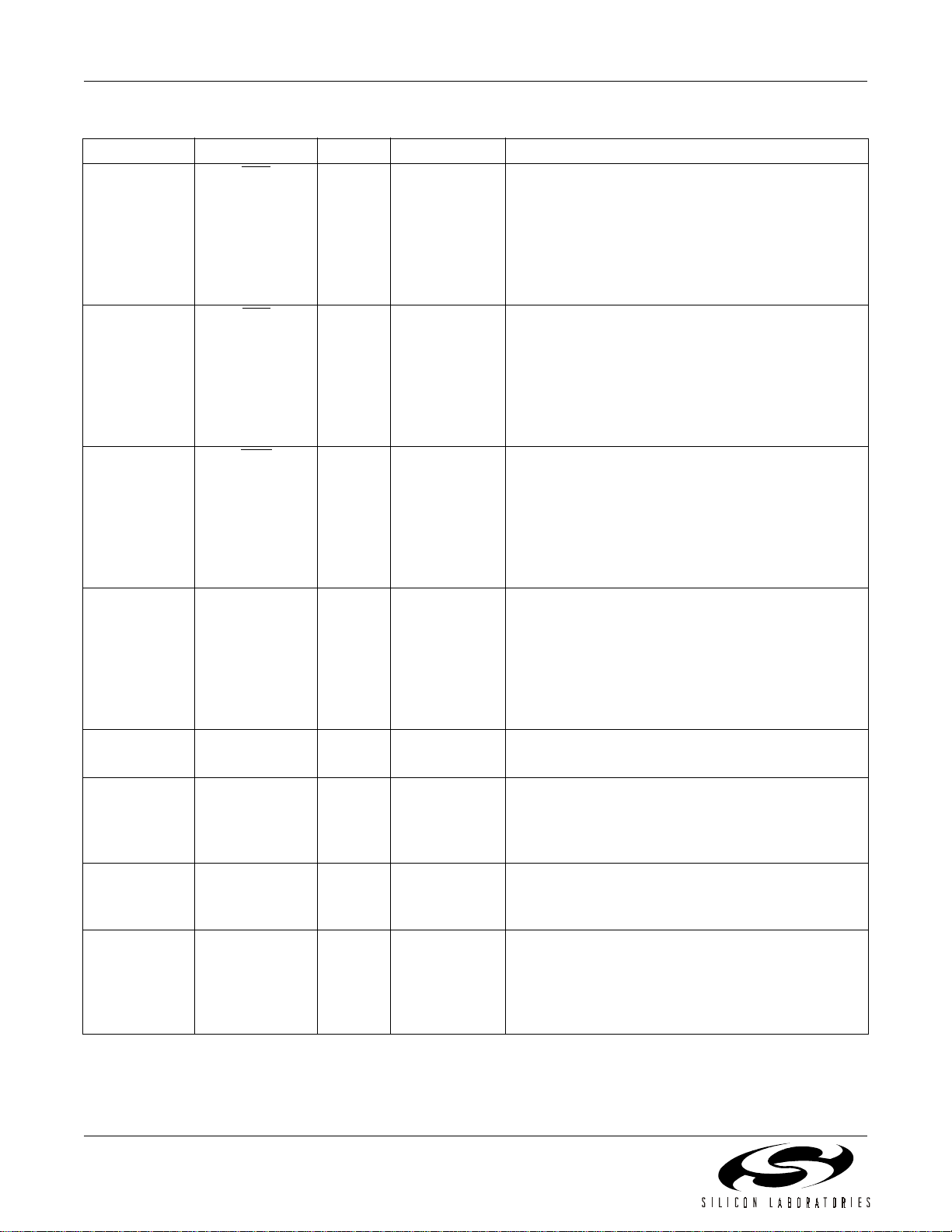
Pin Descriptions: Si5022/23
RATESEL0
RATESEL1
SLICE_LVL
Figure 13. Si5022/23 Pin Configuration
Table 9. Si5022/23 Pin Descriptions
LOS_LVL
REFCLK+
REFCLK-
LOL
NC
1
2
3
4
5
6
7
BER_ALM
BER_LVL
GND
LTR
LOS
DSQLCH
Top View
Pad
VDD
VDD
CLKDSBL
DIN+
CLKOUT+
DIN-
CLKOUT-
22232425262728
141312111098
VDD
VDD
21
REXT
20
RESET/CAL
19
VDD
18
DOUT+
17
DOUT-
16
TDI
15
Si5022/Si5023
Pin # Pin Name I/O Signal Level Description
1,2 RATESEL0,
RATESEL1
ILVTTLData Rate Select.
These pins configure the onboard PLL for clock and
data recovery at one of four user selectable data
rates. See Table 7 for configuration settings.
Note: These inputs have weak internal pull-ups.
3LOS_LVLI LOS Level Control.
The LOS threshold is set by the input voltage level
applied to this pin. Figure 6 on page 12 shows the
input setting to output threshold mapping.
LOS is disabled when the voltage applied is less
than 500 mV.
4SLICE_LVLI Slicing Level Control.
The slicing threshold level is set by applying a voltage to this pin as described in the Slicing Level section of the data sheet. If this pin is tied to GND,
slicing level adjustment is disabled, and the slicing
level is set to the midpoint of the differential input
signal on DIN. Slicing level becomes active when
the voltage applied to the pin is greater than
500 mV.
5,6 REFCLK+,
REFCLK–
I See Table2 Differential Reference Clock (Optional).
When present, the reference clock sets the center
operating frequency of the DSPLL for clock and
data recovery. Tie these pins to ground to configures the DSPLL to operate without an external reference clock.
See Table 8 for typical reference clock frequencies.
Preliminary Rev. 0.46 17
Page 18
Si5022/Si5023
Table 9. Si5022/23 Pin Descriptions (Continued)
Pin # Pin Name I/O Signal Level Description
7
8
9
10 DSQLCH LVTTL Data Squelch.
11,14,18,21,
25
12,13 DIN+,
15 TDI I LVTTL Production Test Input.
16,17 DOUT+,
LOL
LTR
LOS
VDD 2.5 V or
DIN–
DOUT–
OLVTTLLoss-of-Lock.
This output is driven low when the recovered clock
frequency deviates from the reference clock by the
amount specified in Table 4 on page 9. If no external reference is supplied, this signal will be active
when the internal PLL is no longer locked to the
incoming data.
ILVTTLLock-to-Reference.
When this pin is low, the DSPLL will disregard the
data inputs. If an external reference is supplied, the
output clock will be locked to the supplied reference. If no external reference is used, the DSPLL
will lock the control loop until LTR is r eleased.
Note: This input has a weak internal pull-up.
OLVTTLLoss-of-Signal.
This output pin is driven low when the input signal is
below the threshold set via LOS_LVL. The LOS
state will nominally have 3 dB of hysteresis relative
to the level set on LOS_LVL. (LOS operation is
guaranteed only when ac coupling is used on the
clock input.)
When driven high, this pin forces the data present
on DOUT to zero. For normal operation, this pin
should be low. DSQLCH can be used during LOS/
LOL conditions to prevent random data from being
presented to the system.
Note: This input has a weak internal pull-down.
Supply Voltage.
3.3 V
I See Table2 Differential Data Input.
OCMLDi ffer ent ial Data Out put.
Nominally 2.5 V for Si5022 and 3.3 V for Si5023.
Clock and data are recovered from the differential
signal present on these pins. ac coupling is recommended.
This pin is used during production testing and must
be tied to GND for normal operation.
The data output signal is a retimed version of the
data recovered from the signal present on DIN. It is
phase aligned with CLKOUT and is updated on the
rising edge of CLKOUT.
18 Preliminary Rev. 0.46
Page 19

Si5022/Si5023
Table 9. Si5022/23 Pin Descriptions (Continued)
Pin # Pin Name I/O Signal Level Description
19 RESET/CAL I LVTTL Reset/Calibrate.
Driving this input high for at least 1 µS will reset
internal device circuitry. A high to low transition on
this pin will force a DSPLL calibration. For normal
operation, drive this pin low. This pin should be
used to force a DSPLL calibration on power-up to
ensure optimal jitter performance.
Note: This input has a weak internal pull-down.
20 REXT External Bias Resistor.
This resistor is used to establish internal bias currents within the device. This pin must be connected
to GND through a 10 kΩ (1%) resistor.
22,23 CLKOUT–,
CLKOUT+
24 CLKDSBL I LVTTL Clock Disable.
26 BER_LVL I Bit Error Rate Level Control.
27
28 NC No Connect.
GND Pad GND GND Supply Ground.
BER_ALM
OCMLDi ffer en tial Clock Out pu t.
The output clock is recovered from the data signal
present on D IN e xce p t w he n LTR is asserted or t h e
LOL state has been entered.
When this input is high, the CLKOUT output drivers
are disabled. For normal operation, this pin should
be low.
Note: This input has a weak internal pull-down.
The BER threshold level is set by applying a voltage to this pin. The applied voltage is mapped to
one of 64 BER threshold levels. When the BER
exceeds the programmed threshold, BER_ALM is
driven low. If this pin is tied to GND, BER_ALM is
disabled. If it is tied to V
–3
10
BER
OLVTTLBit Error Rate Alarm.
This pin will be driven low to indicate that the BER
threshold set by BER_LVL has been exceeded. The
alarm will clear after the BER rate has improved by
approximately a factor of 2.
Leave this pin unconnected.
Nominally 0.0 V . The GND pad found on the bottom
of the 28-lead micro leaded package (see
Figure 14) must be connected directly to supply
ground. Minimize the ground path inductance for
optimal performance.
DD
, BER_LVL defaults to
Preliminary Rev. 0.46 19
Page 20

Si5022/Si5023
Ordering Guide
Part Number Package Voltage Temperature
Si5022-BM 28-lead MLP 2.5 –40°C to 85°C
Si5023-BM 28-lead MLP 3.3 –40°C to 85°C
Table 10. Ordering Guide
20 Preliminary Rev. 0.46
Page 21

Si5022/Si5023
Package Outline
Figure 14 illustrates the pack age details for the Si 5022 and Si5023. Table 11 lists the values for the dimen sions
shown in the illustration.
A
1
2
3
FOR ODD TERMINAL/SIDE
N
TOP VIEW
C
L
e
D
D/2
D1
D1/2
A
A1
E1/2 E/2
E1 E
L
θ
CC
C
L
e
FOR EV EN TERMINAL/SIDE
bA1
SECTION "C–C"
SCALE: NO NE
BOTTOM VIEW
Figure 14. 28-Lead Micro Leaded Package (MLP)
b
e
(N d–1) Xe
REF.
N
1
2
3
(N d–1) Xe
REF.
Table 11. Package Diagram Dimensions
Controlling Dimension: mm
Symbol Millimeters
Min Nom Max
A — 0.90 1.00
A1 0.00 0.01 0.05
b 0.18 0.23 0.30
D5.00 BSC
D1 4.75 BSC
E5.00 BSC
E1 4.75 BSC
N28
Nd 7
Ne 7
e0.50 BSC
L 0.50 0.60 0.75
θ
12
°
Preliminary Rev. 0.46 21
Page 22

Si5022/Si5023
Contact Information
Silicon Laborato ries Inc.
4635 Boston Lane
Austin, TX 78735
Tel: 1+(512) 416-8500
Fax: 1+(512) 416-9669
Toll Free: 1+(877) 444-3032
Email: productinfo@silabs.com
Internet: www.silabs.com
The information in this document is believed to be accurate in all respects at the time of publication but is subject to change without notice.
Silicon Laboratories assumes no responsibility for errors and omissions, and disclaims responsibility for any consequences resulting from
the use of information included herein. Additionally, Silicon Laboratories assumes no responsibility for the functioning of undescribed features
or parameters. Silicon Laboratories reserves the right to make changes without further notice. Silicon Laboratories makes no warranty, representation or guarantee regarding the suitability of its products for any particular purpose, nor does Silicon Laboratories assume any liability
arising out of the application or use of any product or circuit, and specifically disclaims any and all liability, including without limitation consequential or incidental damages. Silicon Laboratories products are not designed, intended, or authorized for use in applications intended to
support or sustain life, or for any other application in which the failure of the Silicon Laboratories product could create a situation where personal injury or death may occur. Should Buyer purchase or use Silicon Laboratories products for any such unintended or unauthorized application, Buyer shall indemnify and hold Silicon Laboratories harmless against all claims and damages.
Silicon Laboratories, Silicon Labs, and DSPLL are trademarks of Silicon Laboratories Inc.
Other products or brandnames mentioned herein are trademarks or registered trademarks of their respective holders.
22 Preliminary Rev. 0.46
 Loading...