

Page 1
Si5020
SiPHY™ M
ULTI-RATE
SONET/SDH C
LOCK AND DATA RECOVERY
Features
Complete high speed, low power, CDR solution includes the following:
!
Supports OC-48/12/3, STM-16/4/1,
Gigabit Ethernet, and 2.7 Gbps FEC
!
Low Power—270 mW (TYP OC-48)
!
Small Footprint: 4 mm x 4 mm
!
DSPLL™ Eliminates External Loop
Filter Components
!
3.3 V T olerant Control Inputs
!
Exceeds All SONET/SDH
Jitter Specifications
!
Jitter Generation
3.0 mUI
!
Device Power Down
!
Loss-of-Lock Indicator
!
Single 2.5 V Supply
RMS
(TYP)
Applications
!
SONET/SDH/ATM Routers
!
Add/Drop Multiplexers
!
Digital Cross Connects
!
Gigabit Ethernet Interfaces
!
SONET/SDH Test Equipment
!
Optical Transceiver Modules
!
SONET/SDH Regenerators
!
Board Level Serial Links
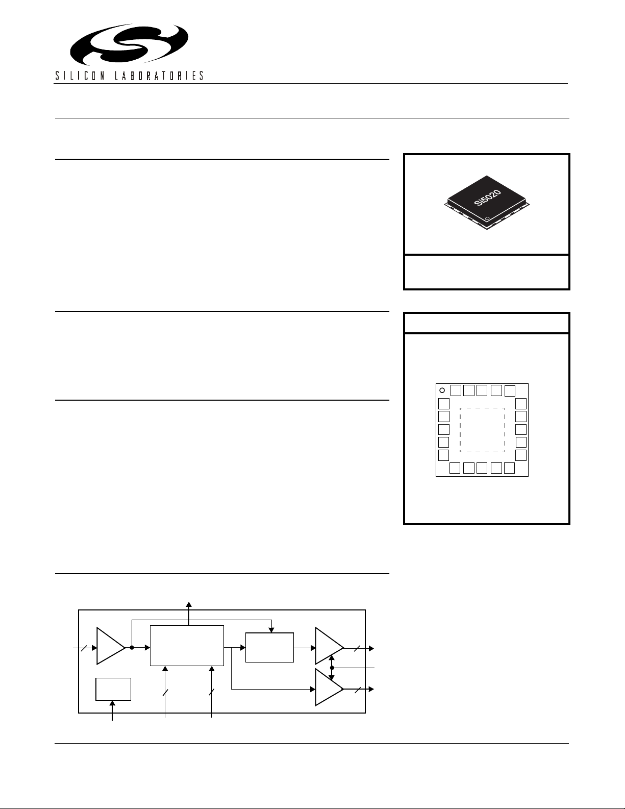
Description
The Si5020 is a fully integrated low-p ower clock and d ata recovery (CDR)
IC designed for high-speed serial communication systems. It extracts
timing information and data from a serial input at OC-48/12/3, STM-16/4/1,
or Gigabit Ethernet (GbE) rates. Support for 2.7 Gbps data streams is also
provided for OC-48/STM-16 applications that employ forward error
correction (FEC). DSPLL™ technology eliminates sensitive noise entry
points thus making the P LL les s susce ptible to board- level inter actio n and
helping to ensure optimal jitter performance.
The Si5020 repres ents a new stan dard in low ji tter, low power, and small
size for high spe ed CDRs. It o perates fr om a singl e 2.5 V supply over the
industrial temperature range (–40°C to 85°C).
Ordering Information:
See page 14.
Pin Assignments
Si5020
RATESEL1
REXT
1
VDD
2
GND
3
REFCLK+
REFCLK–
4
5
6 7 8 9
LOL
Top View
VDD
RATESEL0
GND
Pad
GND
GND
IC
CLKOUT+
CLKOUT–
17181920
16
PWRDN/CAL
15
VDD
14
DOUT+
13
DOUT–
12
11
VDD
10
DIN–
DIN+
Functional Block Diagram
LOL
DIN+
DIN–
BUF
2
Bias
REXT
Preliminary Rev. 0.8 12/00 Copyright © 2000 by Silicon Laboratories Si5020-DS08
This information applies to a product under development. Its characteristics and specifications are subject to change without notice.
DSPLL™
Phase-Locked
Loop
2
RATESEL1–0
2
REFCLK+
REFCLK–
Retimer
BUF
BUF
2
2
DOUT+
DOUT–
PWRDN/CAL
CLKOUT+
CLKOUT–
Page 2

Si5020
2 Preliminary Rev. 0.8
Page 3

Si5020
T
ABLE OF
C
ONTENTS
Section Page
Detailed Block Diagram . . . . . . . . . . . . . . . . . . . . . . . . . . . . . . . . . . . . . . . . . . . . . . . . . . 4
Electrical Specifications . . . . . . . . . . . . . . . . . . . . . . . . . . . . . . . . . . . . . . . . . . . . . . . . . 5
Functional Description . . . . . . . . . . . . . . . . . . . . . . . . . . . . . . . . . . . . . . . . . . . . . . . . . . 9
DSPLL™ . . . . . . . . . . . . . . . . . . . . . . . . . . . . . . . . . . . . . . . . . . . . . . . . . . . . . . . . . . 9
PLL Self-Calibration . . . . . . . . . . . . . . . . . . . . . . . . . . . . . . . . . . . . . . . . . . . . . . . . . . 9
Multi-Rate Operation . . . . . . . . . . . . . . . . . . . . . . . . . . . . . . . . . . . . . . . . . . . . . . . . . 9
Reference Clock Detect . . . . . . . . . . . . . . . . . . . . . . . . . . . . . . . . . . . . . . . . . . . . . . . 9
Forward Error Correction (FEC) . . . . . . . . . . . . . . . . . . . . . . . . . . . . . . . . . . . . . . . . . 9
Lock Detect . . . . . . . . . . . . . . . . . . . . . . . . . . . . . . . . . . . . . . . . . . . . . . . . . . . . . . . . 10
PLL Performance . . . . . . . . . . . . . . . . . . . . . . . . . . . . . . . . . . . . . . . . . . . . . . . . . . . . 10
Power Down . . . . . . . . . . . . . . . . . . . . . . . . . . . . . . . . . . . . . . . . . . . . . . . . . . . . . . . . 11
Device Grounding . . . . . . . . . . . . . . . . . . . . . . . . . . . . . . . . . . . . . . . . . . . . . . . . . . . 11
Bias Generation Circuitry . . . . . . . . . . . . . . . . . . . . . . . . . . . . . . . . . . . . . . . . . . . . . . 11
Differential Input Circuitry . . . . . . . . . . . . . . . . . . . . . . . . . . . . . . . . . . . . . . . . . . . . . . 11
Differential Output Circuitry . . . . . . . . . . . . . . . . . . . . . . . . . . . . . . . . . . . . . . . . . . . . 11
Pin Descriptions: Si5020 . . . . . . . . . . . . . . . . . . . . . . . . . . . . . . . . . . . . . . . . . . . . . . . . . 13
Ordering Guide . . . . . . . . . . . . . . . . . . . . . . . . . . . . . . . . . . . . . . . . . . . . . . . . . . . . . . . . . 15
Package Outline . . . . . . . . . . . . . . . . . . . . . . . . . . . . . . . . . . . . . . . . . . . . . . . . . . . . . . . . 16
Contact Information . . . . . . . . . . . . . . . . . . . . . . . . . . . . . . . . . . . . . . . . . . . . . . . . . . . . . 18
Preliminary Rev. 0.8 3
Page 4
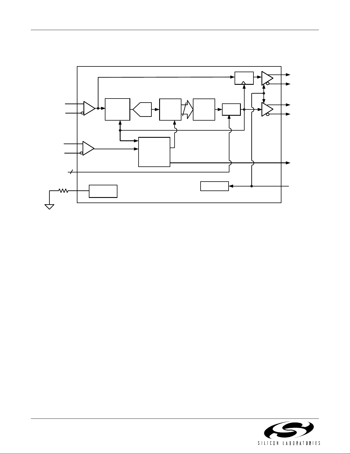
Si5020
Detailed Block Diagram
DIN+
DIN+
DIN–
REFCLK+
REFCLK+
REFCLK–
RATESEL1-0
RATESEL1-0
REXT
Retime
RetimeRetime
DOUT+
DOUT–
c
Phase
Phase
Phase
Detector
Detector
Detector
A/D
DSP
VCO
CLK
Divider
c
CLKOUT+
CLKOUT–
n
Lock
Detector
LOL
2
Bias
Bias
Bias
Generation
Generation
Generation
Ca libra t io n
PWRDN/CAL
Figure 1. Detailed Block Diagram
4 Preliminary Rev. 0.8
Page 5
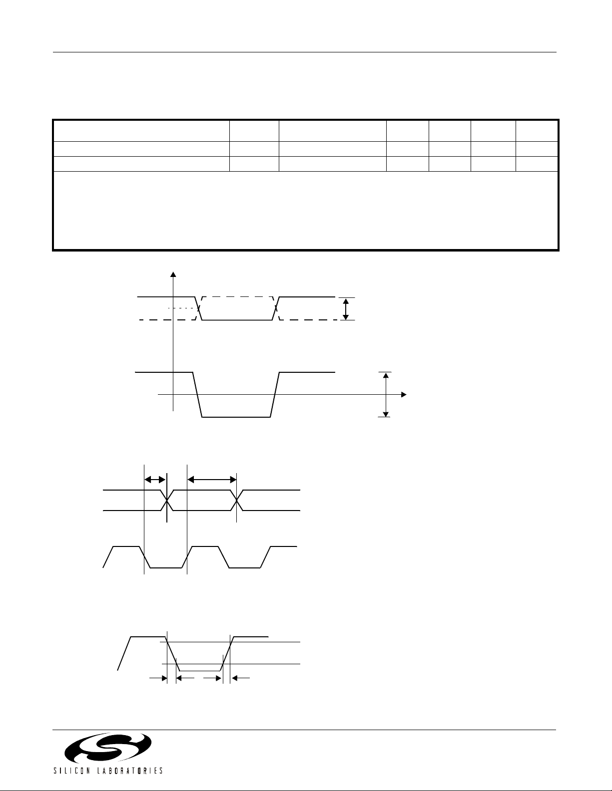
Electrical Specifications
Table 1. Recommended Operating Conditions
Si5020
Parameter
Symbol Test Condition
Ambient Temperature T
Si5020 Supply Voltage
2
V
A
DD
1
Min
Typ
–40 25 85 °C
2.375 2.5 2.625 V
Max
1
Notes:
1. All minimum and maximum specifications are guaranteed and apply across the recommended operating
conditions. Typical values apply at nominal supply voltages and an operating temperature of 25°C unless
otherwise stated.
2. The Si5020 specifications are guaranteed when using the recommended application circuit (including
component tolerance) of Figure 5 on page 9.
V
SIGNAL+
Differential
I/Os
V
ICM,VOCM
SIGNAL–
V
IS
Single-Ended Voltage
(SIGNAL+) – (SIGNAL–)
Differential
Voltage Swing
VID,VOD (V
= 2VIS)
ID
Differential Peak-to-Peak Voltage
t
Unit
DOUT
CLKOUT
DOUT,
CLKOUT
Figure 2. Differential Voltage Measurement (DI N, REFCLK, DOUT, CLKOUT)
t
Cf-D
t
Cr-D
Figure 3. Clock to Data Timing
80%
20%
t
F
t
R
Figure 4. DOUT and CLKOUT Rise/Fall Times
Preliminary Rev. 0.8 5
Page 6
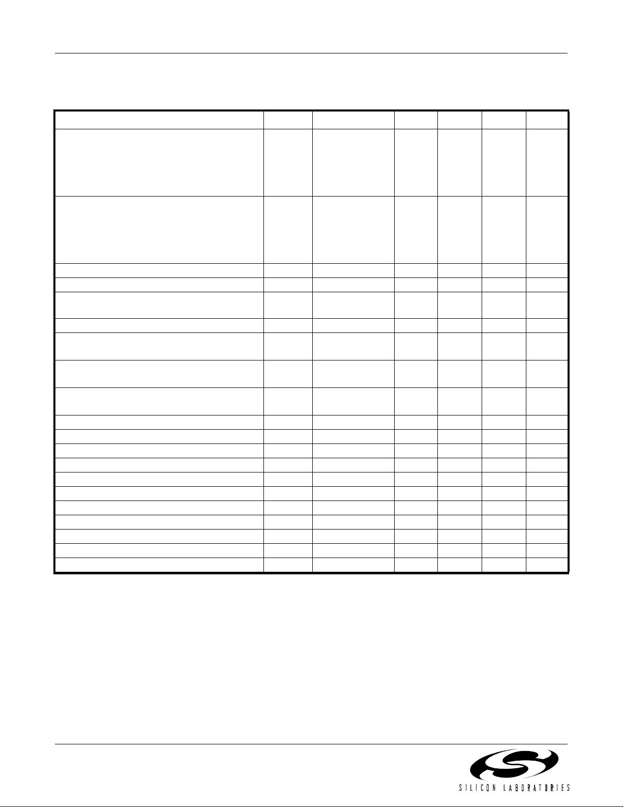
Si5020
Table 2. DC Characteristics
(VDD = 2.5 V ± 5%, TA = –40°C to 85°C)
Parameter Symbol Test Condition Min Typ Max Unit
Supply Current
OC-48 and FEC (2.7 GHz)
GigE
OC-12
OC-3
Power Dissipation
OC-48 and FEC (2.7 GHz)
GigE
OC-12
OC-3
Common Mode Input Voltage (DIN, REFCLK) V
Single Ended Input Voltage (DIN, REFCLK) V
Differential Input Voltage Swing
(DIN, REFCLK)
Input Impedance (DIN, REFCLK) R
Differential Output Voltage Swing
(DOUT)
Differential Output Voltage Swing
(CLKOUT)
Output Common Mode Voltage
(DOUT,CLKOUT)
Output Impedance (DOUT,CLKOUT) R
Output Short to GND (DOUT,CLKOUT) I
Output Short to V
(DOUT,CLKOUT) I
DD
Input Voltage Low (LVTTL Inputs) V
Input Voltage High (LVTTL Inputs) V
Input Low Current (LVTTL Inputs) I
Input High Current (LVTTL Inputs) I
Output Voltage Low (LVTTL Outputs) V
Output Voltage High (LVTTL Outputs) V
Input Impedance (LVTTL Inputs) R
PWRDN/CAL Leakage Current I
I
DD
P
D
varies with V
See Figure 2 100 — 750 mV
See Figure 2 200 — 1500 mV
Line-to-Line 84 100 116 Ω
100 Ω Load
V
ICM
V
IS
ID
IN
OD
Line-to-Line
V
OD
100 Ω Load
Line-to-Line
V
OCM
100 Ω Load
Line-to-Line
OUT
SC(–)
SC(+)
IL
IH
IL
IH
OL
OH
IN
PWRDNVPWRDN
Single-ended 84 100 116 Ω
IO = 2 mA — — 0.4 V
IO = 2 mA 2.0 — — V
DD
—
—
—
—
—
—
—
—
—.80*VDD—V
108
113
117
124
270
283
293
310
118
123
127
134
310
323
333
352
mA
mW
(pk-pk)
TBD 940 TBD mV
(pk-pk)
TBD 900 TBD mV
(pk-pk)
—VDD –
—V
0.20
—25TBDmA
TBD –15 — mA
——.8V
2.0 — — V
——10µA
——10µA
10 — — kΩ
≥ 0.8 V TBD 25 TBD µA
6 Preliminary Rev. 0.8
Page 7

Si5020
Table 3. AC Characteristics (Clock & Data)
(VA 2.5 V ± 5%, TA = –40°C to 85°C)
Parameter Symbol Test Condition Min Typ Max Unit
Output Clock Rate f
Output Rise Time t
Output Fall Time t
Clock to Data Delay
CLK
t
Cr-D
R
F
Figure 4 — 100 TBD ps
Figure 4 — 100 TBD ps
Figure 3
FEC (2.7 GHz)
OC-48
GigE
OC-12
OC-3
Clock to Data Delay
t
Cf-D
Figure 3
FEC (2.7 GHz)
OC-48
Input Return Loss 100 kHz – 2.5 GHz
2.5 GHz – 4.0 GHz
.15 — 2.7 GHz
TBD
TBD
TBD
TBD
TBD
TBD
TBD
18.7
TBD
250
255
500
890
4100
51
50
—
—
TBD
TBD
TBD
TBD
TBD
TBD
TBD
—
—
ps
ps
dB
dB
Preliminary Rev. 0.8 7
Page 8

Si5020
Table 4. AC Characteristics (PLL Characteristics)
(VA 2.5 V ± 5%, TA = –40°C to 85°C)
Parameter Symbol Test Condition Min Typ Max Unit
Jitter Tolerance
(OC-48)*
J
TOL(P–P)
f = 600 Hz 40 TBD — UIp-p
f = 6000 Hz 4 TBD — UIp-p
f = 100 kHz 4 TBD — UIp-p
f = 1 MHz 0.4 TBD — UIp-p
Jitter Tolerance (OC-12 Mode)
*
J
TOL(P–P)
f = 30 Hz 40 TBD — UIp-p
f = 300 Hz 4 TBD — UIp-p
f = 25 kHz 4 TBD — UIp-p
f = 250 kHz 0.4 TBD — UIp-p
Jitter Tolerance (OC-3 Mode)
*
J
TOL(P–P)
f = 30 Hz 60 TBD — UIp-p
f = 300 Hz 6 TBD — UIp-p
f = 6.5 kHz 6 TBD — UIp-p
f = 65 kHz 0.6 TBD — UIp-p
Jitter Tolerance (Gigabit Ethernet)
T
JT(P-P)
IEEE 802.3z Clause 38.68 600 TBD — ps
Receive Data Total Jitter
Tolerance
Jitter Tolerance (Gigabit Ethernet)
D
JT(P-P)
IEEE 802.3z Clause 38.69 370 TBD — ps
Receive Data Deterministic Jitter
Tolerance
RMS Jitter Generation
Peak-to-Peak Jitter Generation
Jitter Transfer Bandwidth
*
*
J
GEN(rms)
*
J
GEN(rms)
J
BW
with no jitter on serial data — 3.0 5.0 mUI
with no jitter on serial data — 25 55 mUI
OC-48 Mode — — 2.0 MHz
OC-12 Mode — — 500 kHz
OC-3 Mode — — 130 kHz
Jitter Transfer Peaking
Acquisition Time T
*
J
AQ
P
After falling edge of
— 0.03 0.1 dB
1.45 1.5 1.7 ms
PWRDN/CAL
From the return of valid
40 60 150 µs
data
Input Reference Clock Duty Cycle C
DUTY
40 50 60 %
Reference Clock Range 19.44 — 168.75 MHz
Input Reference Clock Frequency
C
TOL
–100 — 100 ppm
Tolerance
Frequency Difference at which
LOL TBD 600 TBD ppm
Receive PLL goes out of Lock
(REFCLK compared to the divided
down VCO clock)
Frequency Difference at which
LOCK TBD 300 TBD ppm
Receive PLL goes into Lock (REFCLK compared to the divided
down VCO clock)
*Note: Bellcore specifications: GR-253-CORE, Issue 2, December 1995. Using PRBS 223– 1 data pattern.
8 Preliminary Rev. 0.8
Page 9

Si5020
Table 5. Absolute Maximum Ratings
Parameter Symbol Value Unit
DC Supply Voltage V
LVTTL Input Voltage V
Differential Input Voltages V
DD
DIG
DIF
–0.5 to 2.8 V
–0.3 to 3.6 V
–0.3 to (VDD+ 0.3) V
Maximum Current any output PIN ±50 mA
Operating Junction Temperature T
Storage Temperature Range T
JCT
STG
–55 to 150 °C
–55 to 150 °C
Lead Temperature (soldering 10 seconds) 300 °C
ESD HBM Tolerance (100pf, 1.5 kΩ)1kV
Note: Permanent device damage may occur if the above Absolute Maximum Ratings are exceeded. Functional operation
should be restricted to the conditions as specified in the operational sections of this data sheet. Exposure to absolute
maximum rating conditions for extended periods may affect device reliability.
Table 6. Thermal Characteristics
Parameter Symbol Test Condition Value Unit
Thermal Resistance Junction to Ambient ϕ
LVTTL
Control Inputs
JA
Still Air 38 °C/W
Loss-of-Lock
Indicator
High Speed
Serial Input
System
Reference
Clock
2
LOL
RATESEL1-0
DIN+
DIN–
PWRDN/CAL
DOUT+
DOUT–
Si5020
VDD
0.1
2200pF
20pF
CLKOUT+
CLKOUT–
GND
µµµµ
F
REFCLK+
REFCLK–
ΩΩΩΩ
10k
(1%)
(1%)
(1%)(1%)
REXT
VDD
Figure 5. Si5020 Typical Application Circuit
Recovered
Data
Recovered
Clock
Preliminary Rev. 0.8 9
Page 10

Si5020
Functional Description
The Si5020 utilizes a phase-locked loop (PLL) to
recover a clock s ynchronous to the input data stream .
This clock is used to retime the data, and both the
recovered clock and data are output syn chronously via
current mode logic (CML) drivers. Optimal jitter
performance is obtained by using Silicon Laboratories'
DSPLL™ technology to eliminate the no ise entry poi nts
caused by external PLL loop filter components.
DSPLL
The phase-locked loop structure (shown in Figure 1 o n
page 4) utilizes Silicon Laboratories' DSPLL™
technology to elimin ate the need for external l oop filter
components found in traditional PLL implementations.
This is achieved by using a digital signal processing
(DSP) algorithm to replace the loop filter commonly
found in analog PLL designs . This algorithm pro cesses
the phase detector error term and generates a digital
control value to adjust the frequency of the voltage
controlled oscilla tor (VCO). Bec ause external loo p filter
components are not required, sensitive noise entry
points are eliminated thus making the DSPLL less
susceptible to board-level noise sources that make
SONET/SDH jitter compliance difficult to attain.
™
PLL Self-Calibration
The Si5020 achieves optimal jitter performance by
using self-calibration circuitry to set the loop gain
parameters within the DSPLL. For the self-calibration
circuitry to operate correctly, the power supply voltage
must exceed 2.25 V when calibration occurs. For best
performance, the user should force a self-calibration
once the supply has stabilized on power-up.
A self-calibration can be initiat ed by forcing a high-tolow transition on the power-down control input,
PWRDN/CAL, while a vali d reference clock is supplie d
to the REFCLK input. The PWRDN/CAL input should be
held high at least 1 µS before transitioning low to
guarantee a self-cal ibration. Sev eral applica tion circu its
that could be used to initiate a power- on self-cal ibration
are provided in Silico n Laboratories’ “ AN42: Controlling
the Si5018/20 Self-Calibration.”
Multi-Rate Operation
The Si5020 supports clock and data recovery for OC-48
and STM-16 data streams. In addition, the PLL was
designed to operate at data rates up to 2.7 Gbps to
support OC-48/STM-16 applications that employ
forward error correction (FEC ).
Multi-rate operation is achieved by configuring the
device to divide down the output of the VCO to the
desired data rate. The divide fa ctor is confi gured by the
RATESEL0-1 pins. Th e RATESEL0-1 configuration and
associated data rates are given in Table 7.
Table 7. Multi-Rate Configurati o n
OC-48
RATESEL
[0:1]
00 2.488 Gbps — 2.67 Gbps 1
10 1.244 Gbps 1.25 Gbps — 2
01 622.08 Mbps — — 4
11 155.52 Mbps — — 16
SONET/
SDH
Gigabit
Ethernet
with
15/14
FEC
CLK
Divider
Reference Clock Detect
The Si5020 uses the reference clock to cente r the VCO
output frequency so that clock and data can be
recovered from the input data stream. The device will
self configure for o peration with one of three refe rence
clock frequencies. This eliminates the need to externally
configure the device to operate with a particular
reference clock.
The reference clock centers the VCO for a nominal
output of between 2.5 GHz and 2.7 Ghz. The VCO
frequency is centered at 16, 32, or 128 times the
reference clock frequency. Detection circuitry
continuously monitors the reference clock input to
determine whether the dev ice should be configured for
a reference clock that is 1/16, 1/32, or 1/128 the
nominal VCO output. Approximate reference clock
frequencies for some target applications are given in
Table 8.
Table 8. Typical REFCLK Frequencies
SONET/SDH
19.44 MHz 19.53 MHz 20.83 MHz 128
77.76 MHz 78.125 MHz 83.31 MHz 32
155.52 MHz 156.25 MHz 166.63 MHz 16
Gigabit
Ethernet
SONET/
SDH with
15/14 FEC
Ratio of
VCO to
REFCLK
10 Preliminary Rev. 0.8
Page 11

Si5020
Forward Error Correction (FEC)
The Si5020 supports FEC in SONET OC-48 (SDH
STM-16) application s for data rates up to 2.7 Gbps. In
FEC applications, the appropriate reference clock
frequency is determined by dividing the input data rate
by 16, 32, or 128. For example, if an FEC code is use d
that produces a 2.70 Gbps data rate, the required
reference clock would be 168 .75 MHz, 84.375 MHz, or
21.09 MHz.
Lock Detect
The Si5020 provides lock-detect circuitry that i ndicates
whether the PLL has ac hieved frequency lock with th e
incoming data. The ci rcuit compare s the frequency of a
divided down version of the recovered clock with the
frequency of the supplied refer ence clock (REFCLK). If
the recovered clock frequen cy deviates from that of th e
reference clock by the amount specified in Table 4 on
page 8, the PLL i s decla red ou t of lock , and th e loss -oflock (LOL) pin is asserted “high.” In this state, the
DSPLL will periodically try to reacquire lock with the
incoming data stream. During reacquisition, the
recovered clock, CLKOUT, will drift over a ±600 ppm
range relative to the su pplied re ference clock. Th e LOL
output will remain asserted until the recovered clock
frequency is within the REFCLK frequency by the
amount specified in Table 4.
Note: LOL is not asserted during PWRDN/CAL.
PLL Performance
The PLL implementation used in the Si5020 is fully
compliant with the jitter specifications proposed for
SONET/SDH equipment by Bellcore GR-253-CORE,
Issue 2, December 1995 and ITU-T G.958.
Jitter Tolerance
The Si5020’s tolerance to input jitter exceeds that of the
Bellcore/ITU mask shown in Figure 6. This mask
defines the level of peak-to-peak sinusoid jitter that
must be tolerated when applied to the differential data
input of the device.
Note: There are no entries in the mask table for the data rate
corresponding to OC-24 as that rate is not specified by
either GR-253 or G.958.
Sinusoidal
Input
Jitter (UI p-p)
Slope = 20 dB/Decade
15
1.5
0.15
f0 f1 f2 f3 ft
Frequency
SONET
Data RateF0(Hz)F1(Hz)F2(Hz)F3(kHz)Ft(kHz)
OC-48 10 600 6000 100 1000
OC-12 10 30 300 25 250
OC-3 10 30 300 6.5 65
Figure 6. Jitter Tolerance Specification
Jitter Transfer
The Si5020 is fu lly compl iant w ith the rel evant Bell core /
ITU specifications related to SONET/SD H jitter transfer.
Jitter transfer is defined as the ratio of output signal jitter
to input signal jitter as a functi on of jitte r freq uency ( see
Figure 7). These meas urem ents are made with an input
test signal that is degraded with sinusoidal jitter whose
magnitude is defined by the mask in Figure 6.
Jitter Generation
The Si5020 exceeds all r elevant specifications for jitter
generation proposed for SONET/SDH equipment. The
jitter generation specification defines the amount of jitter
that may be present on the recovered clock and data
outputs when a ji tter free input signal is provi ded. The
Si5020 typically generates less than 3.0 mUI rms of
jitter when presented with jitter-free input data.
Preliminary Rev. 0.8 11
Page 12

Si5020
Jitter
Transfer
0.1 dB
Acceptable
Range
Fc
Frequency
20 dB / Decade
Slope
SONET
Data RateFc(kHz)
OC-48 2000
OC-12 500
OC-3 130
Figure 7. Jitter Transfer Specification
Power Down
The Si5020 provides a power do wn pin, PWRDN/CAL,
that disables the output drivers (DOUT, CLKOUT).
When the PWRDN/CAL pin is driven “high”, the positi ve
and negative terminals of CLKOUT and DOUT are each
tied to VDD through 100 Ω on-chip resistors. This
feature is useful in reducing power consumption in
applications that employ redundant serial channels.
When PWRDN/CAL is released (set to “low”) the d igital
logic resets to a kn own initia l conditi on, reca librate s the
DSPLL, and will begin to lock to the data stream.
Device Grounding
The Si5020 uses the GND pad on the bottom of the 20pin micro leaded package (MLP) for device ground. This
pad should be connected di rectly to the analog supply
ground. See Figures 10 and 11 for the ground (GND)
pad location.
Bias Generation Circuitry
The Si5020 makes use of an external resistor to set
internal bias currents. The external resistor allows
precise generation of bias currents which significantly
reduces power consumption versus traditional
implementations tha t use an internal resistor. The bias
generation circuitry requires a 10 kΩ (1%) resistor
connected between REXT and GND.
Differential Input Circuitry
The Si5020 provides d ifferentia l inputs f or both the hig h
speed data (DIN) and the reference clock (REFCLK)
inputs. An example termination for these inputs is
shown in Figure 8. In applications where direct DC
coupling is possible, the 0.1 µF capacitors may be
omitted. The DIN and REFCLK input amplifiers require
an input signal with a minimum differenti al peak- to -peak
voltage listed in Table 2 on page 6.
DIN+,
DIN–,
Si5020
2.5 kΩΩΩΩ
Differential Driver
0.1 µ
0.1 µ
µF
µ µ
µF
µ µ
Zo = 50 ΩΩΩΩ
Zo = 50 ΩΩΩΩ
REFCLK+
REFCLK–
Figure 8. Input Termination for DIN and REFCLK (AC Coupled)
12 Preliminary Rev. 0.8
VDD
2.5 kΩΩΩΩ10 kΩΩΩΩ
10 kΩΩΩΩ
GND
102 ΩΩΩΩ
Page 13

Si5020
Differential Output Circuitry
The Si5020 utilizes a current mode logic (CML) architecture to output both the recovered clock (CLKOUT) and data
(DOUT). An example of output termination with AC coupling is shown in Figure 9. In applications in which direct DC
coupling is possible, the 0.1 µF capacitors may be omitted. The differential peak-to-peak voltage swing of the CML
architecture is listed in Table 2 on page 6.
Si5020
100 ΩΩΩΩ
100 ΩΩΩΩ
VDD
VDD
DOUT+,
CLKOUT+
DOUT–,
CLKOUT–
0.1 µµµµF
0.1 µµµµF
Zo = 50 ΩΩΩΩ
Zo = 50 ΩΩΩΩ
VDD
50 ΩΩΩΩ
50 ΩΩΩΩ
VDD
Figure 9. Output Termination for DOUT and CLKOUT (AC Coupled)
Preliminary Rev. 0.8 13
Page 14

Si5020
Pin Descriptions: Si5020
RATESEL1
RATESEL0
GND
CLKOUT+
CLKOUT–
17181920
16
10
15
14
13
12
11
DIN–
PWRDN/CAL
VDD
DOUT+
DOUT–
VDD
REXT
VDD
GND
REFCLK+
REFCLK–
1
2
3
4
5
6 7 8 9
LOL
GND
VDD
Pad
GND
DIN+
Top View
Figure 10. Si5020 Pin Configuration
Table 9. Si5020 Pin Descriptions
Pin # Pin Name I/O Signal Level Description
1REXT External Bias Resistor.
This resistor is used by onboard circuitry to establish bias currents within the device. This pin must
be connected to GND through a 10 kΩ (1%) resis-
tor.
4, 5 REFCLK+,
REFCLK–
I See Table 2 Differential Reference Clock.
The reference clock sets the initial operating frequency used by the onboard PLL for clock and data
recovery. Additionally , the reference clock is used to
derive the clock output when no data is present.
6LOLOLVTTLLoss of Lock.
This output is driven high when the recovered clock
frequency deviates from the reference clock by the
amount specified in Table 4 on page 8.
9, 10 DIN+, DIN– I See Table 2 Differential Data Input.
Clock and data are recovered from the differential
signal present on these pins.
12, 13 DOUT–,
DOUT+
OCMLDifferential Data Output.
The data output signal is a retimed version of the
data recovered from the signal present on DIN. It is
phase aligned with CLKOUT and is updated on the
rising edge of CLKOUT.
14 Preliminary Rev. 0.8
Page 15

Table 9. Si5020 Pin Descriptions (Continued)
Pin # Pin Name I/O Signal Level Description
Si5020
15 PWRDN/CAL I LVTTL
16, 17 CLKOUT–,
CLKOUT+
19, 20 RATESEL1,
RATESEL0
2, 7, 11, 14 VDD 2.5 V Supply Voltage.
3, 8, 18, and
GND Pad
GND GND Supply Ground.
OCMLDifferential Clock Output.
ILVTTLData Rate Select.
Power Down.
To shut down the high-speed outputs and reduce
power consumption, hold this pin high. For normal
operation, hold this pin low.
Calibration.
To initiate an internal self-calibration, force a highto-low transition on this pin. (See "PLL Self-Calibration‚" on page 10.)
Note: This input has a weak internal pulldown.
The output clock is recovered from the data signal
present on DIN. In the absence of data, the output
clock is derived from REFCLK.
These pins configure the onboard PLL for clock and
data recovery at one of four user selectable data
rates. See Table 7 for configuration settings.
Note: These inputs have weak internal pulldowns.
Nominally 2.5 V.
Nominally 0.0 V . The GND pad found on the bottom
of the 20-pin micro leaded package (see Figure 11)
must be connected directly to supply ground.
Preliminary Rev. 0.8 15
Page 16

Si5020
Ordering Guide
Table 10. Ordering Guide
Part Number Package Temperature
Si5020-BM 20-pin MLP –40°C to 85°C
16 Preliminary Rev. 0.8
Page 17

Si5020
Package Outline
Figure 11 illustrates the package detail s for the Si5020. Table 11 lists the values for the dimension s shown in the
illustration.
56
0.50 DIA.
TOP VIEW
A
1
2
3
D
D1
N
D1/2
2X
D/2
A
C0.25
E1/2 E/2
E1 E
0.252XB
C
BOTTOM VIEW
10
0.05
A
A2
C
A1
A3
4X P
R
4X P
4X Q
4
0.10 BAMC
b
D2
D2/2
8.
N
1
2
(Ne-1)X e
3
E2
REF.
0.20
C
2X
FOR ODD TERMINAL/SIDE FOR EVEN TERMINAL/SIDE
B
2X
e
AC0.20
C
L
TERMINAL TIP
CC
C
L
4
e
Figure 11. 20-pin Micro Leaded Package (MLP)
Table 11. Package Diagram Dimensions
B
b
SECTION "C-C"
SCALE: NONE
L
0
C
SEATING
11
A1
1.
2.
3.
4.
PLANE
NOTES:
DIE THICKNESS ALLOW ABLE IS 0.305mm MAXIMUM(.012 INCHES MAXIMUM)
DIMENSIONING & TOLERANCES C ON FOR M T O ASME Y14.5M. - 1994.
N IS THE NUMBER OF TERMINALS.
Nd IS THE NUMBER OF TERMINALS IN X-DIRECTION &
Ne IS THE NUMBER OF TERMINALS IN Y-DIRECTION.
DIMENSION b APPLIES TO PLATED TERMINAL AND IS MEASURED
BETWEEN 0.20 AND 0.25mm FROM T ERM INAL TIP.
5.
THE PIN #1 IDENTIFIER MUST BE EXISTED ON THE TOP SURF ACE O F TH E
PACKAGE BY USING INDENTATION MARK O R OT HER FEAT URE O F PAC KAG E BOD Y.
EXACT SHAPE AND SIZE OF THIS FEATURE IS OPTIONAL.
6.
7. ALL DIMENSIONS ARE IN MILLIMETERS.
THE SHAPE SHOWN ON FOU R CO RN ERS AR E NO T AC TUAL I/O.
8.
PACKAGE W AR PAG E MAX 0.05mm.9.
APPLIED FOR EXPOSED PAD AND T ERMINALS.
10.
EXCLUDE EMBEDDING PART O F EXPO SED
PAD FROM MEASURING.
APPLIED ONLY FOR TERM INALS.
11.
e
(Nd-1)Xe
REF.
E2/2
Symbol Millimeters Symbol Millimeters
Min Nom Max Min Nom Max
A — 0.85 1.00 E1 3.75 BSC
A1 0.00 0.01 0.05 E2 1.95 2.10 2.25
A2 — 0.65 0.80 N 20
A3 0.20 REF Nd 5
b 0.23 0.28 0.35 Ne 5
D 4.00 BSC L 0.50 0. 60 0.75
D1 3.75 BSC P 0.24 0.42 0.60
D2 1.95 2.10 2.25 Q 0.30 0.40 0.65
e 0.50 BSC R 0.13 0.17 0.23
E 4.00 BSC θ ——12°
Preliminary Rev. 0.8 17
Page 18

Si5020
Contact Information
Silicon Laborato ries Inc.
4635 Boston Lane
Austin, TX 78735
Tel: 1+(512) 416-8500
Fax: 1+(512) 416-9669
Toll Free: 1+(877) 444-30 32
Email: productinfo@silabs.com
Internet: www.silabs.com
The information in this document is believed to be accurate in all respects at the time of publication but is subject to change without notice.
Silicon Laboratories assumes no responsibility for errors and omissions, and disclaims responsibility for any consequences resulting from
the use of information included herein. Additionally, Silicon Laboratories assumes no responsibility for the functioning of undescribed features
or parameters. Silicon Laboratories reserves the right to make changes without further notice. Silicon Laboratories makes no warranty, representation or guarantee regarding the suitability of its products for any particular purpose, nor does Silicon Laboratories assume any liability
arising out of the application or use of any product or circuit, and specifically disclaims any and all liability, including without limitation consequential or incidental damages. Silicon Laboratories products are not designed, intended, or authorized for use in applications intended to
support or sustain life, or for any other application in which the failure of the Silicon Laboratories product could create a situation where personal injury or death may occur. Should Buyer purchase or use Silicon Laboratories products for any such unintended or unauthorized application, Buyer shall indemnify and hold Silicon Laboratories harmless against all claims and damages.
Silicon Laboratories, Silicon Labs, and DSPLL are trademarks of Silicon Laboratories Inc.
Other products or brandnames mentioned herein are trademarks or registered trademarks of their respective holders.
18 Preliminary Rev. 0.8
 Loading...