

Page 1
C/W
查询72021供应商
Dual N-Channel 30-V (D-S) MOSFET with Schottky Diode
Si4830ADY
Vishay Siliconix
PRODUCT SUMMARY
V
(V) r
DS
30
0.022 @ VGS = 10 V 7.5
0.030 @ VGS = 4.5 V 6.5
(W) I
DS(on)
SCHOTTKY PRODUCT SUMMARY
VSD (V)
V
(V)
DS
30 0.50 V @ 1.0 A 2.0
Ordering Information: Si4830ADY—E3 (Lead Free)
Diode Forward Voltage
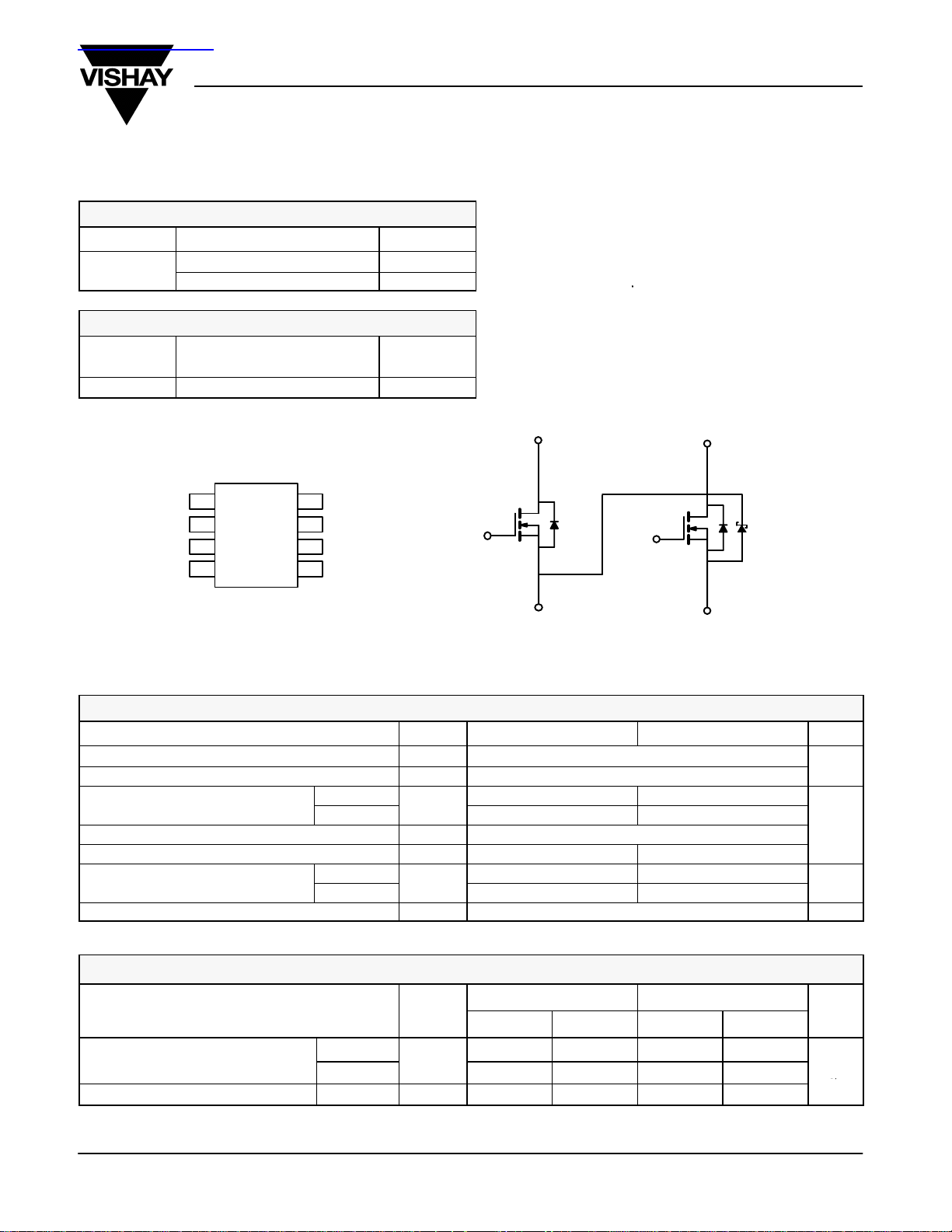
SO-8
S
1
1
G
2
1
S
3
2
G
4
2
Top View
Si4830ADY-T1—E3 (Lead Free with Tape and Reel)
D
8
1
D
7
1
D
6
2
D
5
2
FEATURES
(A)
D
D LITTLE FOOTr Plus Schottky
D Si4830DY Pin Compatible
D PWM Optimized
D 100% R
Tested
g
APPLICATIONS
D Asymmetrical Buck-Boost DC/DC Converter
I
(A)
F
D
G
1
N-Channel MOSFET
1
G
2
S
1
D
2
S
2
N-Channel MOSFET
Schottky Diode
ABSOLUTE MAXIMUM RATINGS (TA = 25_C UNLESS OTHERWISE NOTED)
Parameter Symbol 10 secs Steady State Unit
Drain-Source Voltage V
Gate-Source Voltage V
a
TA = 25_C
TA = 70_C
TA = 25_C
TA = 70_C
P
a
Continuous Drain Current (TJ = 150_C)
Pulsed Drain Current I
Continuous Source Current (Diode Conduction)
Maximum Power Dissipation
Operating Junction and Storage Temperature Range TJ, T
_
a
I
DM
I
DS
GS
D
S
D
stg
7.5 5.7
6.0 4.6
1.7 0.9
2.0 1.1
1.3 0.7
30
"20
30
−55 to 150 _C
THERMAL RESISTANCE RATINGS
MOSFET Schottky
Parameter Symbol
Maximum Junction-to-Ambient
Maximum Junction-to-Foot (Drain) Steady-State R
Notes
a. Surface Mounted on 1” x 1” FR4 Board.
a
t v 10 sec
Steady-State
R
thJA
thJF
Typ Max Typ Max
52 62.5 53 62.5
93 110 93 110
35 40 35 40
V
A
W
Unit
_C/W
Document Number: 72021
S-32621—Rev. D, 29-Dec-03
www.vishay.com
1
Page 2
Si4830ADY
b
b
DS
,
GS
,
D
VDD = 15 V, RL = 15 W
g
rm
Vishay Siliconix
MOSFET SPECIFICATIONS (TJ = 25_C UNLESS OTHERWISE NOTED).
Parameter Symbol Test Condition Min TypaMax Unit
Static
Gate Threshold Voltage V
Gate-Body Leakage I
Zero Gate Voltage Drain Current I
On-State Drain Current
b
Drain-Source On-State Resistance
Forward Transconductance
b
Diode Forward Voltage
Dynamic
a
Total Gate Charge Q
Gate-Source Charge Q
Gate-Drain Charge Q
Gate Resistance R
Turn-On Delay Time t
Rise Time t
Turn-Off Delay Time t
Fall Time t
Source-Drain Reverse Recovery Time t
Notes
a. Guaranteed by design, not subject to production testing.
b. Pulse test; pulse width v
300 ms, duty cycle v 2%.
GS(th)
GSS
DSS
I
D(on)
r
DS(on)
g
V
d(on)
d(off)
fs
SD
g
gs
gd
g
r
f
rr
VDS = 30 V, VGS = 0 V, TJ = 85_C
VDS = VGS, I
VDS = 0 V, V
VDS = 30 V, VGS = 0 V
V
DS
= 250 mA 0.8 3.0 V
D
= "20 V "100 nA
GS
Ch-1
Ch-2 100
_
Ch-1
Ch-2 2000
= 5 V, VGS = 10 V 20 A
VGS = 10 V, ID = 7.5 A 0.017 0.022
VGS = 4.5 V, ID = 6.5 A 0.024 0.030
VDS = 15 V, ID = 7.5 A 19 S
IS = 1 A, VGS = 0 V
V
= 15 V, VGS = 4.5 V, ID = 7.5 A
DS
VDD = 15 V, RL = 15 W
ID ^ 1 A, V
= 10 V, Rg = 6 W
GEN
IF = 1.7 A, di/dt = 100 A/ms
Ch-1
Ch-2 0.47 0.5
Ch-1
Ch-2 32 55
1
15
0.75 1.2
7 11
2.9
2.5
0.5 1.5 2.4 W
9 15
10 17
19 30
9 15
35 55
mA
W
V
nC
ns
SCHOTTKY SPECIFICATIONS (TJ = 25_C UNLESS OTHERWISE NOTED)
Parameter Symbol Test Condition Min Ty p Max Unit
Forward Voltage Drop V
Maximum Reverse Leakage Current I
Junction Capacitance C
F
rm
T
www.vishay.com
2
IF = 1.0 A 0.47 0.50
IF = 1.0 A, TJ = 125_C 0.36 0.42
Vr = 30 V 0.004 0.100
Vr = 30 V, TJ = 100_C 0.7 10
Vr = −30 V, TJ = 125_C 3.0 20
Vr = 10 V
50 pF
Document Number: 72021
S-32621—Rev. D, 29-Dec-03
V
mA
Page 3

Si4830ADY
Vishay Siliconix
TYPICAL CHARACTERISTICS (25_C UNLESS NOTED) MOSFET
− Drain Current (A)I
D
W )
− On-Resistance (r
DS(on)
30
25
20
15
10
VGS = 10 thru 5 V
5
0
0246810
VDS − Drain-to-Source Voltage (V)
4 V
3 V
On-Resistance vs. Drain Current
0.040
0.030
VGS = 4.5 V
Output Characteristics Transfer Characteristics
0.020
0.010
VGS = 10 V
30
25
20
15
10
− Drain Current (A)I
D
5
0
012345
1200
960
720
480
C − Capacitance (pF)
240
TC = 125_C
25_C
VGS − Gate-to-Source Voltage (V)
Capacitance
C
iss
C
oss
C
rss
−55_C
0.000
0 5 10 15 20 25 30
10
VDS = 15 V
I
= 7.5 A
8
6
4
− Gate-to-Source Voltage (V)
GS
2
V
0
Document Number: 72021
S-32621—Rev. D, 29-Dec-03
D
0 3 6 9 12 15
− Drain Current (A)
I
D
Gate Charge
Qg − Total Gate Charge (nC)
− On-Resistance r
(Normalized)
DS(on)
0
0 5 10 15 20 25 30
VDS − Drain-to-Source Voltage (V)
On-Resistance vs. Junction Temperature
1.8
VGS = 10 V
I
= 7.5 A
D
1.6
1.4
1.2
1.0
0.8
0.6
−50 −25 0 25 50 75 100 125 150
T
− Junction Temperature (_C)
J
www.vishay.com
3
Page 4

Si4830ADY
Vishay Siliconix
TYPICAL CHARACTERISTICS (25_C UNLESS NOTED) MOSFET
Source-Drain Diode Forward Voltage On-Resistance vs. Gate-to-Source Voltage
W )
− On-Resistance (r
DS(on)
0.06
0.05
0.04
ID = 7.5 A
0.03
0.02
0.01
20
10
TJ = 150_C
1
− Source Current (A)I
S
TJ = 25_C
0.1
0.0 0.2 0.4 0.6 0.8 1.0 1.2
VSD − Source-to-Drain Voltage (V) VGS − Gate-to-Source Voltage (V)
Threshold Voltage
0.4
0.2
ID = 250 mA
−0.0
−0.2
Variance (V)V
GS(th)
−0.4
−0.6
−0.8
−50 −25 0 25 50 75 100 125 150
TJ − Temperature (_C)
Safe Operating Area, Junction-to-Foot
100
Limited by r
10
DS(on)
0.00
100
80
60
Power (W)
40
20
0246810
Single Pulse Power, Junction-to-Ambient
0
−3
10
1 ms
−2
10
Time (sec)
−1
11010
www.vishay.com
4
1
− Drain Current (A)I
D
0.1
0.01
0.1 1 10 100
TC = 25_C
Single Pulse
VDS − Drain-to-Source Voltage (V)
10 ms
100 ms
1 s
10 s
dc
Document Number: 72021
S-32621—Rev. D, 29-Dec-03
Page 5

Si4830ADY
Vishay Siliconix
TYPICAL CHARACTERISTICS (25_C UNLESS NOTED) MOSFET
Normalized Thermal Transient Impedance, Junction-to-Ambient
2
1
Duty Cycle = 0.5
0.2
Notes:
P
DM
t
1
t
1. Duty Cycle, D =
2. Per Unit Base = R
3. TJM − TA = PDMZ
4. Surface Mounted
2
thJA
t
t
thJA
100
1
2
= 93_C/W
(t)
0.1
Thermal Impedance
Normalized Effective Transient
0.01
10
0.1
0.05
0.02
−4
Single Pulse
−3
10
−2
10
−1
1 10 60010
Square Wave Pulse Duration (sec)
2
1
0.1
Thermal Impedance
Normalized Effective Transient
0.01
10
Duty Cycle = 0.5
0.2
0.1
0.05
0.02
−4
Single Pulse
10
Normalized Thermal Transient Impedance, Junction-to-Foot
−3
−2
10
−1
Square Wave Pulse Duration (sec)
11010
Document Number: 72021
S-32621—Rev. D, 29-Dec-03
www.vishay.com
5
Page 6

Si4830ADY
Vishay Siliconix
TYPICAL CHARACTERISTICS (25_C UNLESS NOTED) SCHOTTKY
− Reverse Current (mA)I
R
Reverse Current vs. Junction Temperature
20
10
1
0.1
0.01
0.001
0.0001
0 25 50 75 100 125 150
30 V
24 V
TJ − Temperature (_C)
Capacitance
200
160
120
Forward Voltage Drop
10
TJ = 150_C
TJ = 25_C
− Forward Current (A)I
F
1
0.0 0.3 0.6 0.9 1.2 1.5
VF − Forward Voltage Drop (V)
80
C − Capacitance (pF)
40
0
0 6 12 18 24 30
C
oss
VDS − Drain-to-Source Voltage (V)
www.vishay.com
6
Document Number: 72021
S-32621—Rev. D, 29-Dec-03
 Loading...