

©1994 Burr-Brown Corporation PDS-1214C Printed in the U.S.A. May, 1995
Wide-Bandwidth,
DC RESTORATION CIRCUIT
APPLICATIONS
● BROADCAST/HDTV EQUIPMENT
● TELECOMMUNICATIONS EQUIPMENT
● HIGH-SPEED DATA ACQUISITION
● CAD MONITORS/CCD IMAGE
PROCESSING
● NANO SECOND PULSE INTEGRATOR/
PEAK DETECTORS
● PULSE CODE MODULATOR/
DEMODULATOR
● COMPLETE VIDEO DC LEVEL
RESTORATION
● SAMPLE/HOLD AMPLIFIER
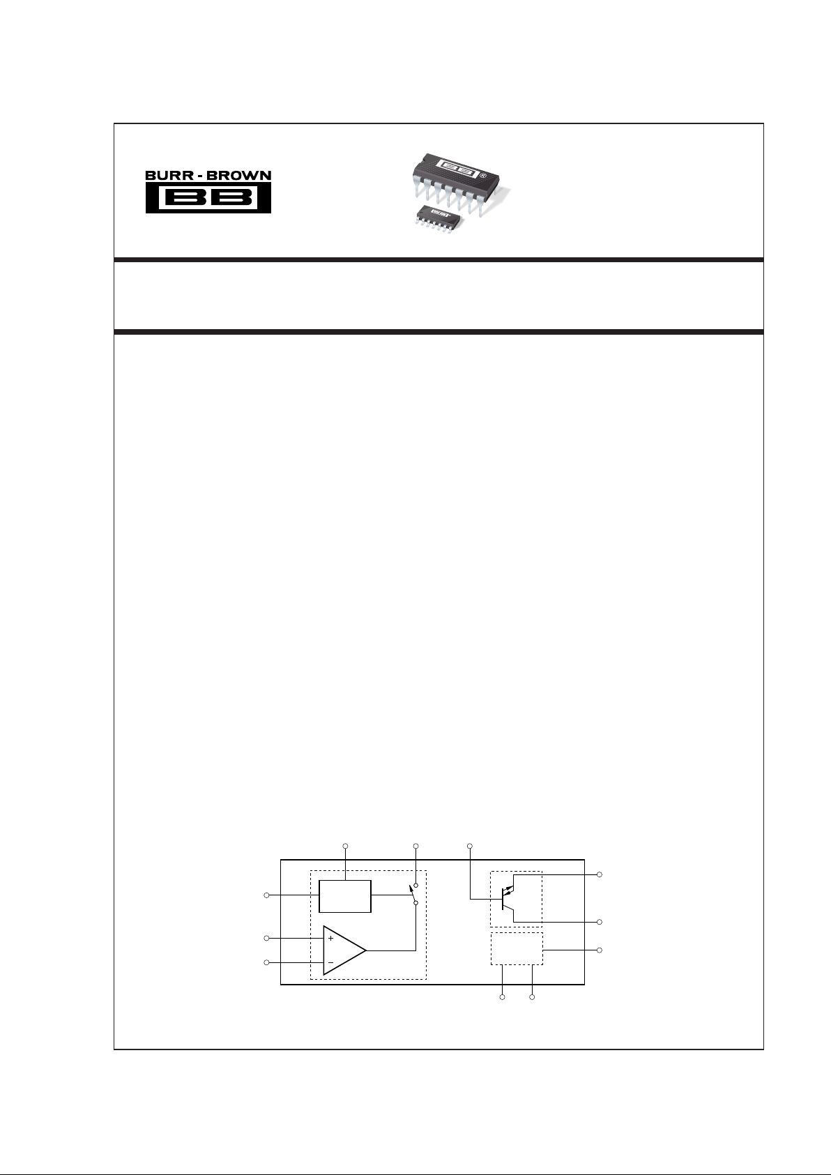
optimized for low input bias current. The sampling
comparator has two identical high-impedance inputs
and a current source output optimized for low output
bias current and offset voltage; it can be controlled by
a TTL-compatible switching stage within a few
nanoseconds. The transconductance of the OTA and
sampling comparator can be adjusted by an external
resistor, allowing bandwidth, quiescent current, and
gain tradeoffs to be optimized.
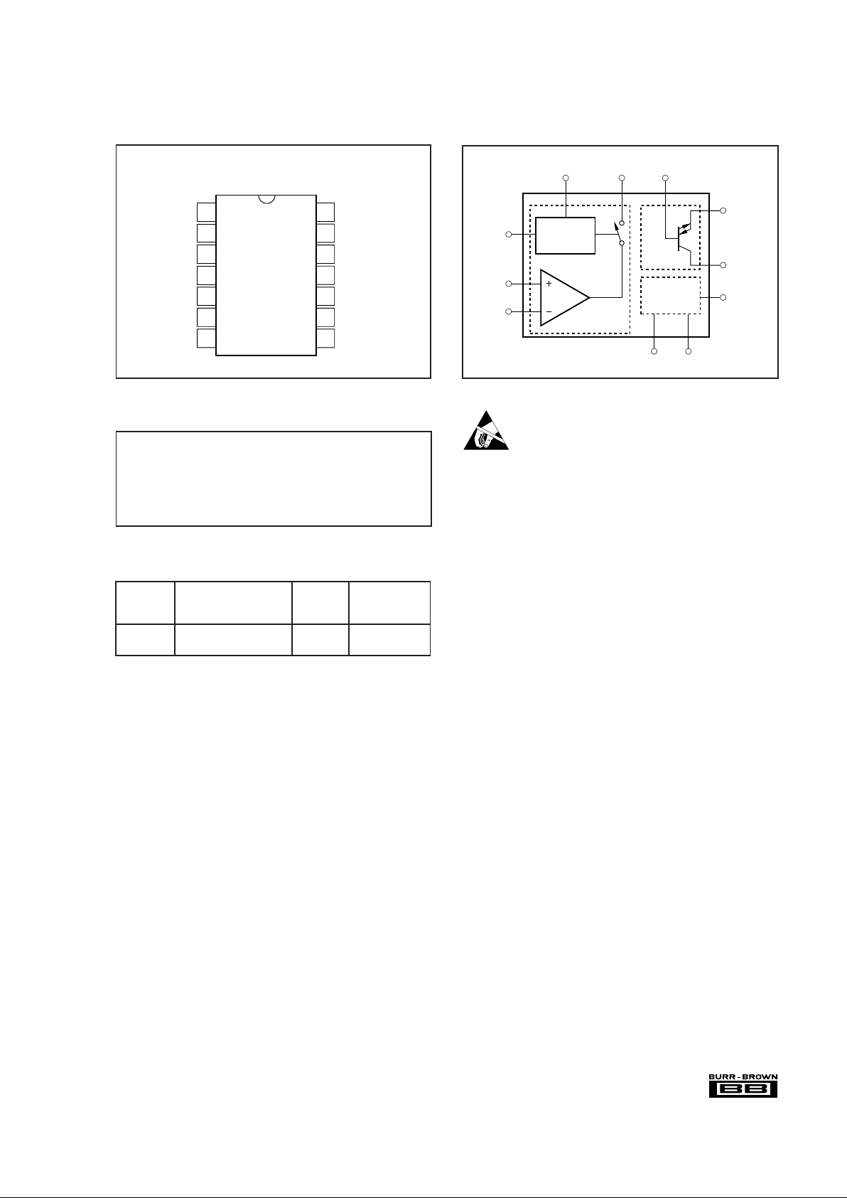
The SHC615 is available in SO-14 surface mount and
14-pin plastic DIPs, and is specified over the extended temperature range of –40°C to +85°C.
FEATURES
● PROPAGATION DELAY: 2.2ns
● BANDWIDTH: OTA: 750MHz
Comparator: 280MHz
● LOW INPUT BIAS CURRENT: –0.3µA
● SAMPLE/HOLD
SWITCHING TRANSIENTS: +1/–7mV
● SAMPLE/HOLD
FEEDTHROUGH REJECTION: 100dB
● CHARGE INJECTION: 40fC
● HOLD COMMAND DELAY TIME: 3.8ns
● TTL/CMOS HOLD CONTROL
DESCRIPTION
The SHC615 is a complete subsystem for very fast
and precise DC restoration, offset clamping, and low
frequency hum suppression of wideband amplifiers or
buffers. Designed to stabilize the performance of
video signals, it can also be used as a sample/hold
amplifier, high-speed integrator, or peak detector for
nanosecond pulses. A wideband Operational
Transconductance Amplifier (OTA) with a high-impedance cascode current source output and fast sampling comparator set a new standard for high-speed
applications. Both can be used as stand-alone circuits
or combined to form a more complex signal processing stage. The self-biased, bipolar OTA can be viewed
as an ideal voltage-controlled current source and is
Switching
Stage
Biasing
SHC615
∞
SOTA
OTA
1
12
2
11
10
7
943
13 5
+V
CC–VCC
IQ Adjust
Collector (I
OUT
)
Emitter
C
HOLD
BaseGround
Hold Control
S/H
In+
S/H
In–
Sampling
Comparator (SC)
®
SHC615
SHC615
SHC615
International Airport Industrial Park • Mailing Address: PO Box 11400, Tucson, AZ 85734 • Street Address: 6730 S. Tucson Blvd., Tucson, AZ 85706 • Tel: (520) 746-1111 • Twx: 910-952-1111
Internet: http://www.burr-brown.com/ • FAXLine: (800) 548-6133 (US/Canada Only) • Cable: BBRCORP • Telex: 066-6491 • FAX: (520) 889-1510 • Immediate Product Info: (800) 548-6132
2
®
SHC615
SHC615AP, AU
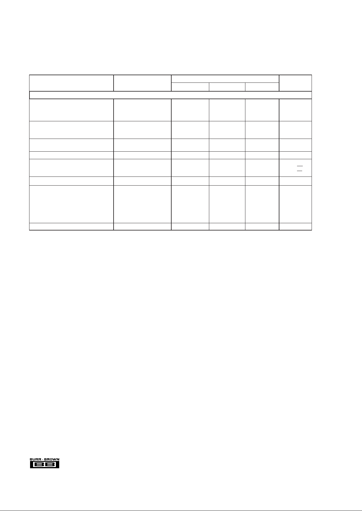
PARAMETER CONDITIONS MIN TYP MAX UNITS
OTA
OFFSET VOLTAGE, V
E
at VB = 0
Initial 8 ±40 mV
vs Temperature 40 µV/°C
vs Supply (tracking) V
CC
= ±4.5V to ±5.5V 50 55 dB
B-INPUT BIAS CURRENT
Initial –0.3 ±0.9 µA
vs Temperature 1 nA/°C
C-OUTPUT BIAS CURRENT, I
C
at VB = 0
Initial –200 –77 +100 µA
B-INPUT IMPEDANCE 4.4 MΩ
INPUT NOISE
Voltage Noise Density, B-to-E f
OUT
= 100kHz to 100MHz 2.2 nV/√Hz
Voltage Noise Density, B-to-C f
OUT
= 100kHz to 100MHz 4.5 nV/√Hz
INPUT VOLTAGE RANGE ±3.4 V
OUTPUT
Output Voltage Compliance ±3.2 V
C-Current Output ±18 ±20 mA
E-Current Output ±18 ±20 mA
C-Output Impedance 0.5 MΩ
E-Output Impedance 12 Ω
Open-Loop Gain 96 dB
TRANSCONDUCTANCE Small Signal, <200mV 70 mA/V
The information provided herein is believed to be reliable; however, BURR-BROWN assumes no responsibility for inaccuracies or omissions. BURR-BROWN
assumes no responsibility for the use of this information, and all use of such information shall be entirely at the user’s own risk. Prices and specifications are
subject to change without notice. No patent rights or licenses to any of the circuits described herein are implied or granted to any third party. BURR-BROWN
does not authorize or warrant any BURR-BROWN product for use in life support devices and/or systems.
DC SPECIFICATIONS
At VCC = ±5V, R
LOAD
= 100Ω, RQ = 300Ω, RIN = 150Ω and TA = +25°C, unless otherwise specified.
3
®
SHC615
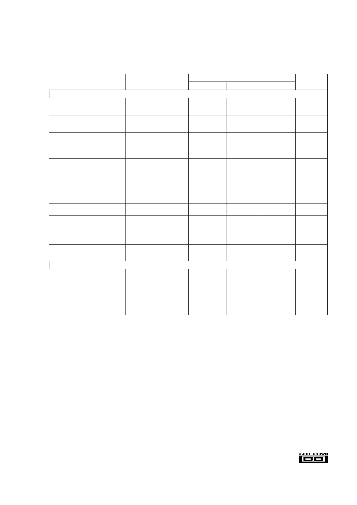
DC SPECIFICATIONS (CONT)
At VCC = ±5V, R
LOAD
= 1kΩ, RQ = 300Ω, and TA = +25°C, unless otherwise specified.
SHC615AP, AU
PARAMETER CONDITIONS MIN TYP MAX UNITS
COMPARATOR
INPUT BIAS CURRENT
Initial 1.0 ±5 µA
vs Temperature –2.3 nA/°C
C-OUTPUT BIAS CURRENT
Initial ±10 ±50 µA
vs Temperature ±13 nA/°C
INPUT IMPEDANCE
Input Impedance 0.2 MΩ
INPUT NOISE
Voltage Noise Density f
OUT
= 100kHz to 100MHz 5 nV/√Hz
INPUT VOLTAGE RANGE
Input Voltage Range ±3.0 V
Common-Mode Input Range ±3.2 V
OUTPUT
Output Voltage Compliance ±3.5 V
C-Current Output ±2.5 ±3.2 mA
C-Output Impedance 620 || 2 kΩ || pF
Open-Loop Gain 83 dB
TRANSCONDUCTANCE
Transconductance 22 mA/V
HOLD CONTROL
Logic 1 Voltage +2 +V
CC
+0.6 V
Logic 0 Voltage 0 0.8 V
Logic 1 Current V Hold Control = 5.0V 1 µA
Logic 0 Current V Hold Control = 0.8V 0.05 µA
TRANSFER CHARACTERISTICS
Charge Injection Track-To-Hold 40 fC
Feedthrough Rejection Hold Mode –100 dB
COMPLETE SHC615
POWER SUPPLY
Rated Voltage ±5V
Derated Performance ±4.5 ±5.5 V
Quiescent Current R
Q
= 300Ω±12 ±15 ±18 mA
Quiescent Current Range Programmable (Useful Range) ±3 to ±36 mA
TEMPERATURE RANGE
Operating –40 +85 °C
Storage –40 +125 °C
4
®
SHC615
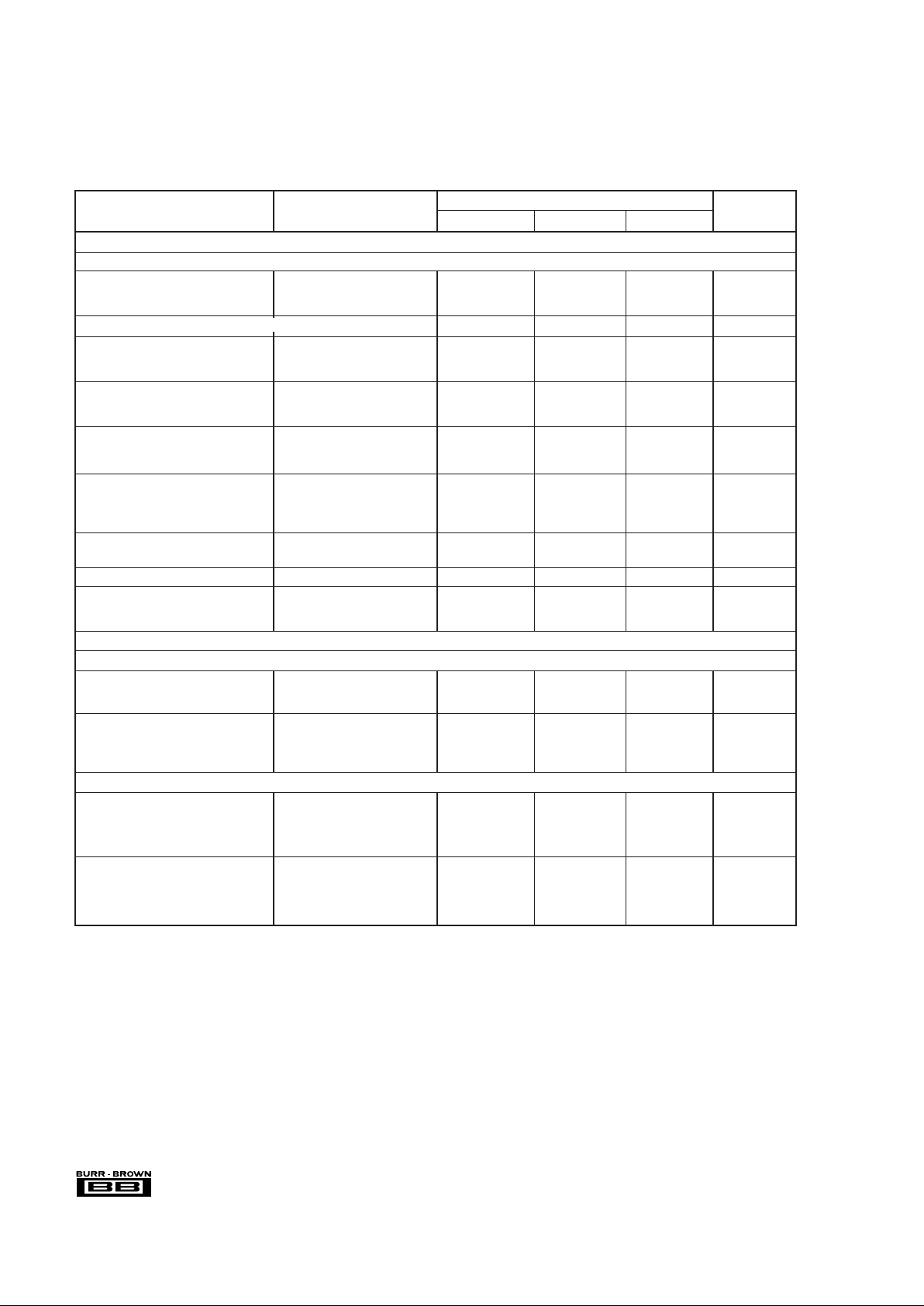
AC SPECIFICATIONS
At VCC = ±5V, R
LOAD
= 100Ω, R
SOURCE
= 50Ω, RQ = 300Ω, and TA = +25°C, unless otherwise specified.
SHC615AP, AU
PARAMETER CONDITIONS MIN TYP MAX UNITS
FREQUENCY DOMAIN
OTA
LARGE-SIGNAL BANDWIDTH V
OUT
= 5.0Vp-p 430 MHz
(–3dB), (B-to-E) V
OUT
= 2.8Vp-p 540 MHz
V
OUT
= 1.4Vp-p 620 MHz
SMALL-SIGNAL BANDWIDTH B-TO-E V
OUT
= 0.2Vp-p 520 MHz
DIFFERENTIAL GAIN (B-TO-E) f = 4.43MHz, V
OUT
= 0.7Vp-p,
R
L
= 150Ω 1.8 %
R
L
= 500Ω 0.1 %
DIFFERENTIAL PHASE f = 4.43MHz, V
OUT
= 0.7Vp-p,
R
L
= 150Ω 0.07 °
(B-to-E) R
L
= 500Ω 0.01 °
HARMONIC DISTORTION (B-TO-E) f = 30MHz, V
OUT
= 1.4Vp-p
Second Harmonic –50 dBc
Third Harmonic –46 dBc
LARGE SIGNAL BANDWIDTH
(–3dB), (B-to-C) V
OUT
= 5.0Vp-p 250 MHz
V
OUT
= 2.8Vp-p 580 MHz
V
OUT
= 1.4Vp-p 750 MHz
SMALL SIGNAL BANDWIDTH
B-to-C V
OUT
= 0.2Vp-p 680 MHz
COMPARATOR Sample Mode
BANDWIDTH I
OUT
= 4mAp-p 240 MHz
(–3dB) I
OUT
= 2mAp-p 270 MHz
I
OUT
= 1mAp-p 280 MHz
TIME DOMAIN
OTA
RISE TIME 2Vp-p Step, 10% to 90%
B-to-E 1.1 ns
B-to-C 1.2 ns
SLEW RATE 2Vp-p,B-to-E 1800 V/µs
B-to-C 1700 V/µs
5Vp-p,B-to-E 3300 V/µs
B-to-C 3000 V/µs
COMPARATOR
RISE TIME
10% to 90%, RL = 50Ω, I
OUT
= ±2mA
(Sample Mode) C
LOAD
= 1pF 2.5 ns
SLEW RATE
10% to 90%, RL = 50Ω, I
OUT
= ±2mA
(Sample Mode) C
LOAD
= 1pF 0.95 mA/ns
DYNAMIC CHARACTERISTICS
Propagation Delay Time t
PDH
, VOD = 200mV 2.2 ns
Propagation Delay Time t
PDL
, VOD = 200mV 2.15 ns
Delay Time Sample-to-Hold 3.8 ns
Hold-to-Sample 3.0 ns
5
®
SHC615
PIN CONFIGURATION
Top View DIP, SO-14
BLOCK DIAGRAM
IQ Adjust
Emitter, E
Base, B
C
HOLD
–V
CC
NC
Hold Control
NC
+V
CC
I
OUT
, Collector, C
S/H In–
S/H In+
Ground
NC
1
2
3
4
5
6
7
•
14
13
12
11
10
9
8
SHC615
Power Supply Voltage (±VCC)..............................................................±6V
Input Voltage
(1)
........................................................................ ±VCC ±0.7V
Operating Temperature ....................................................–40°C to +85°C
Storage Temperature ...................................................... –40°C to +125°C
Junction Temperature .................................................................... +150°C
Lead Temperature (soldering, 10s) ...............................................+300°C
Hold Control..............................................................–0.5V to +V
CC
+0.7V
NOTE: (1) Inputs are internally diode-clamped to ±V
CC
.
ABSOLUTE MAXIMUM RATINGS
ELECTROSTA TIC
DISCHARGE SENSITIVITY
Any integrated circuit can be damaged by ESD. Burr-Brown
recommends that all integrated circuits be handled with appropriate precautions. Failure to observe proper handling and
installation procedures can cause damage.
ESD damage can range from subtle performance degradation
to complete device failure. Precision integrated circuits may
be more susceptible to damage because very small parametric
changes could cause the device not to meet published specifications.
PACKAGE
DRAWING TEMPERATURE
PRODUCT PACKAGE NUMBER
(1)
RANGE
SHC615AP Plastic 14-Pin DIP 010 –40°C to +85°C
SHC615AU
SO 14-Lead Surface-Mount
235 –40°C to +85°C
NOTE: (1) For detailed drawing and dimension table, please see end of data
sheet, or Appendix C of Burr-Brown IC Data Book.
PACKAGE/ORDERING INFORMATION
Switching
Stage
Biasing
SHC615
∞
SOTA
OTA
1
12
2
11
10
7
943
13 5
+V
CC–VCC
IQ Adjust
Collector
(I
OUT
)
Emitter
C
HOLD
BaseGround
Hold
Control
S/H
In+
S/H
In–
Sampling
Comparator (SC)
6
®
SHC615
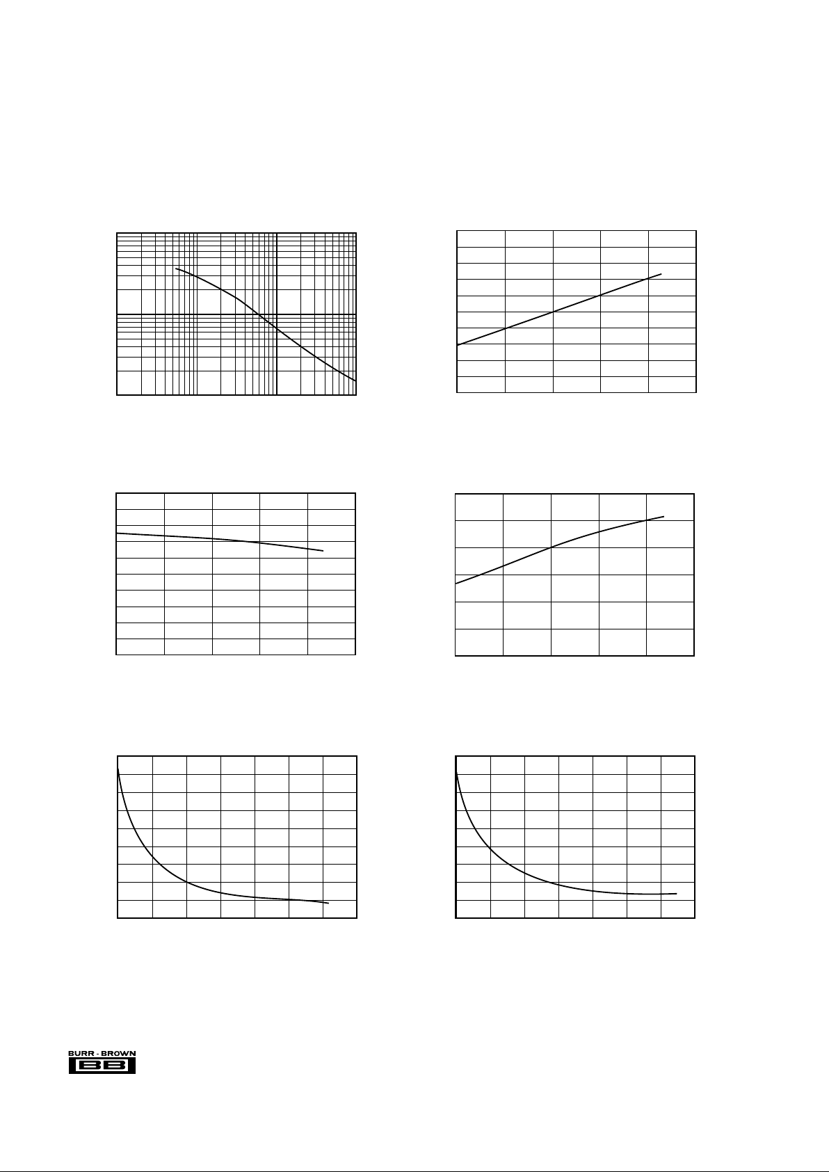
TYPICAL PERFORMANCE CURVES
At RQ = 300Ω, TA = +25°C, VCC = ±5V, unless otherwise noted.
OPERATIONAL TRANSCONDUCTANCE AMPLIFIER
SHC615 TOTAL QUIESCENT CURRENT vs R
Q
100
10
1
10 100 1000 10000
R
Q
(Ω)
Total Quiescent Current, I
Q
(mA)
TOTAL QUIESCENT CURRENT vs TEMPERATURE
1.50
1.40
1.30
1.20
1.10
1.00
0.90
0.80
0.70
0.60
0.50
–25 0 25 50 75 100
Temperature (C°)
Total Quiescent Current, I
Q
(Normalized)
OTA B-INPUT BIAS CURRENT vs TEMPERATURE
0.0
–0.1
–0.2
–0.3
–0.4
–0.5
–0.6
–0.7
–0.8
–0.9
–1.0
–25 0 25 50 75 100
Temperature (C°)
OTA-B Input Bias Current (µA)
OTA-B INPUT OFFSET VOLTAGE vs TEMPERATURE
12
10
8
6
4
2
0
–25 0 25 50 75 100
Temperature (C°)
OTA-B Input Offset Voltage (mV)
RE = 100Ω
OTA-B INPUT RESISTANCE vs
TOTAL QUIESCENT CURRENT
18
16
14
12
10
8
6
4
2
0
5 10152025303540
Total Quiescent Current, I
Q
(mA)
OTA-B Input Resistance (MΩ)
OTA-E OUTPUT RESISTANCE vs
TOTAL QUIESCENT CURRENT
45
40
35
30
25
20
15
10
5
0
4 9 14 19 24 29 34 39
Total Quiescent Current, I
Q
(mA)
OTA-E Output Resistance (Ω)

7
®
SHC615
TYPICAL PERFORMANCE CURVES (CONT)
At RQ = 300Ω, TA = +25°C, VCC = ±5V, unless otherwise noted.
OTA-C OUTPUT RESISTANCE vs
TOTAL QUIESCENT CURRENT
1.8
1.6
1.4
1.2
1
0.8
0.6
0.4
0.2
0
5 10152025303540
Total Quiescent Current, I
Q
(mA)
OTA-C Output Resistance (MΩ)
OTA-C OUTPUT BIAS CURRENT vs TEMPERATURE
–60
–65
–70
–75
–80
–85
–90
–95
–100
Temperature (°C)
–40 –20 0 20 40 60 80 100
OTA-C Output Bias Current (µA)
OTA TRANSFER CHARACTERISTICS
vs INPUT VOLTAGE
25
20
15
10
5
0
–5
–10
–15
–20
–25
–3.5 –3 –2.5 –2 –1.5 –1 –0.5 0 0.5 1 1.5 2 2.5 3 3.5
OTA-B Input Voltage (V)
OTA-C Output Current (mA)
IQ = ±14mA
IQ = ±25mA
IQ = ±5mA
V
IN
150Ω
V
OUT
100Ω
R
C
100Ω
R
E
OTA
OTA TRANSFER CHARACTERISTIC vs INPUT VOLTAGE
25
20
15
10
5
0
–5
–10
–15
–20
–25
–0.2 –0.15 –0.1 –0.05 0 0.05 0.1 0.15 0.2
OTA-B Input Voltage (V)
OTA-C Output Current (mA)
IQ = ±25mA
IQ = ±14mA
IQ = ±5mA
V
IN
150Ω
V
OUT
100Ω
R
C
OTA
OTA TRANSCONDUCTANCE vs
TOTAL QUIESCENT CURRENT
100
90
80
70
60
50
40
30
20
10
0
0 ±5 ±10 ±15 ±20 ±25 ±30
Total Quiescent Current, I
Q
(mA)
Transconductance (mA/V)
Small Signal
(<200mV)
OTA-TRANSCONDUCTANCE vs FREQUENCY
100
80
60
40
20
0
1.0 10k 100k 1M 10M 100M 1G
Frequency (Hz)
Transconductance (mA/V)
IQ = ±25mA
IQ = ±5mA
IQ = ±14mA
Large Signal
(>200mV)

8
®
SHC615
OTA-E VOLTAGE NOISE SPECTRAL DENSITY
45
40
35
30
25
20
15
10
5
0
100 1k 10k 100k
Frequency (Hz)
TYPICAL PERFORMANCE CURVES (CONT)
At RQ = 300Ω, TA = +25°C, VCC = ±5V, unless otherwise noted.
OTA-C Voltage Noise Density (nV/√Hz)
OTA-E Voltage Noise Density (nV/√Hz)
2.2nV/√Hz
OTA-E FREQUENCY RESPONSE
20
10
0
–10
–20
–30
300k 1M 10M 100M 1G
Frequency (Hz)
Gain (dB)
0.6Vp-p
0.2Vp-p
150Ω
V
OUT
50Ω
12
2
3
V
IN
2.8Vp-p
1.4Vp-p
5Vp-p
OTA
OTA-E SMALL SIGNAL PULSE RESPONSE
150
100
50
0
–50
–100
–150
0 20406080100
Time (ns)
OTA-E Output Voltage (mV)
R
IN
= 150Ω, RL = 100Ω, VIN = 200mVp-p,
t
RISE
= t
FALL
= 1.5ns (Generator)
OTA-E LARGE SIGNAL PULSE RESPONSE
3
2
1
0
–1
–2
–3
0 20406080100
Time (ns)
OTA-E Output Voltage (V)
RIN = 150Ω, RL = 100Ω, VIN = 4Vp-p,
t
RISE
= t
FALL
= 1.5ns (Generator)
OTA-C VOLTAGE NOISE SPECTRAL DENSITY
90
80
70
60
50
40
30
20
10
0
100 1k 10k 100k
Frequency (Hz)
4.5nV/√Hz
20
10
0
–10
–20
–30
–40
OTA-C FREQUENCY RESPONSE
300k 1M 10M 100M 1G
Frequency (Hz)
Gain (dB)
150Ω
V
OUT
50Ω
100Ω
100Ω
12
2
3
V
IN
5Vp-p
2.8Vp-p
1.4Vp-p
0.6Vp-p
0.2Vp-p
OTA

9
®
SHC615
TYPICAL PERFORMANCE CURVES (CONT)
At RQ = 300Ω, TA = +25°C, VCC = ±5V, unless otherwise noted.
SAMPLING COMPARATOR
OTA-C SMALL SIGNAL PULSE RESPONSE
150
100
50
0
–50
–100
–150
0 20406080100
Time (ns)
OTA-C Output Voltage (mV)
RIN = 150Ω, RE = 100Ω, RC = 100Ω,
V
IN
= 200mVp-p, t
RISE
= t
FALL
= 1.5ns (Generator)
OTA-C LARGE SIGNAL PULSE RESPONSE
3
2
1
0
–1
–2
–3
0 20406080100
Time (ns)
OTA-C Output Voltage (V)
RIN = 150Ω, RE = 100Ω, RC = 100Ω,
V
IN
= 4Vp-p, t
RISE
= t
FALL
= 1.5ns (Generator)
OTA-E HARMONIC DISTORTION vs FREQUENCY
–45
–46
–47
–48
–49
–50
–51
–52
–53
1M 10M 100M
Frequency (Hz)
OTA-E Harmonic Distortion (dBc)
2f
3f
RE = 100Ω
OTA-C HARMONIC DISTORTION vs FREQUENCY
0
–5
–10
–15
–20
–25
–30
–35
–40
–45
–50
1M 10M 100M
V
OUT
= 1.4Vp
R
E
= RC = 100Ω
Frequency (Hz)
OTA-C Harmonic Distortion (dBc)
2f
3f
INPUT BIAS CURRENT vs TEMPERATURE
1.4
1.2
1.0
0.8
0.6
0.4
0.2
0
–40 –20
Temperature (C°)
Input Bias Current (µA)
S/H In+
S/H In–
0 20406080
100
OUTPUT BIAS CURRENT vs TEMPERATURE
20
15
10
5
0
0
5
–10
–40
Temperature (°C)
Output Bias Current (µA)
–20 0 20 40 60 80 100

10
®
SHC615
TYPICAL PERFORMANCE CURVES (CONT)
At RQ = 300Ω, TA = +25°C, VCC = ±5V, unless otherwise noted.
INPUT RESISTANCE vs TOTAL QUIESCENT CURRENT
0.7
0.6
0.5
0.4
0.3
0.2
0.1
0
5 10152025303540
Total Quiescent Current, I
Q
(mA)
Input Resistance (MΩ)
TRANSCONDUCTANCE vs
TOTAL QUIESCENT CURRENT
40
30
20
10
0
0 5 10 15 20 25
Total Quiescent Current, I
Q
(mA)
Transconductance (mA/V)
TRANSFER CHARACTERISTICS
6
4
2
0
–2
–4
–6
–0.2 –0.15 –0.1 –0.05 0 0.05 0.1 0.15 0.2
Input Voltage (V)
Comparator Output Current (mA)
IQ = ±25mA
IQ = ±14mA
IQ = ±5mA
TRANSCONDUCTANCE vs INPUT VOLTAGE
50
40
30
20
10
0
–10
–0.2 –0.15 –0.1 –0.05 0 0.05 0.1 0.15 0.2
Input Voltage (V)
Comparator Transconductance (mA/V)
IQ = ±25mA
IQ = ±14mA
IQ = ±5mA
PROPAGATION DELAY vs TOTAL QUIESCENT CURRENT
3
4
3.5
3
2.5
2
1.5
1
8 131821283338
Total Quiescent Current, I
Q
(mA)
Delay (ns)
Pos
Neg
COMMON-MODE REJECTION vs FREQUENCY
0
–20
–40
–60
–80
–100
Frequency (Hz)
1M300k 10M 100M 1G
Common-Mode Rejection (dB)

11
®
SHC615
TYPICAL PERFORMANCE CURVES (CONT)
At RQ = 300Ω, TA = +25°C, VCC = ±5V, unless otherwise noted.
PROPAGATION DELAY vs OVERDRIVE
3
2.5
2
1.5
1
0.5
0
0 200 400 600 800 100 1200
∆ Input Voltage (mV)
V
OD
V
OD
V
OD
GND
Pos
Neg
Propogation Delay (ns)
100Ω
100Ω
4
11
SC
10
PROPAGATION DELAY TIME vs TEMPERATURE
3
2.8
2.6
2.4
2.2
2
1.8
1.6
–40 –20 0 20 40 60 80 100 120
Temperature (°C)
Propagation Delay (ns)
Pos
Neg
PROPAGATION DELAY vs LOAD CAPACITANCE
40
35
30
25
20
15
10
5
0
0 100 200 300 400 500 600 700 800 900 1000
Capacitive Load, C
L
(pF)
Propagation Delay (ns)
Pos
Neg
4
10
11
SC
C
LOAD
PROPAGATION DELAY vs SLEW RATE
4
3.5
3
2.5
2
1.5
1
(0)
500
(2)
250
(4)
160
(6)
120
(8)96(10)80(12)68(14)60(16)53(18)48(20)
Slew Rate (V/µs)
(Rise Time (ns))
Propagation Delay (ns)
Pos
Neg
VIN = 1.2Vpp
V
REF
–0.6V
+0.6V
V
OD
= 1.2Vp-p
COMPARATOR RESPONSE TO A
2ns ANALOG INPUT PULSE
150
100
50
0
–50
–100
–150
Output Voltage (mV)
Time (ns)
0 20406080100
I
OUT
= 4mAp-p
R
L
= 50Ω
COMPARATOR RESPONSE TO A
10ns ANALOG INPUT PULSE
150
100
50
0
–50
–100
–150
Output Voltage (mV)
Time (ns)
0 20406080100
I
OUT
= 4mAp-p
R
L
= 50Ω

12
®
SHC615
TYPICAL PERFORMANCE CURVES (CONT)
At RQ = 300Ω, TA = +25°C, VCC = ±5V, unless otherwise noted.
100Ω 150Ω
200Ω
200Ω
50Ω
TTL
50Ω
100Ω
TTL
Comparator
CD74HCT
4
7
11
10
SWITCHING TRANSIENTS TEST CIRCUITS
SC
Switching Transients (mV)
5
0
–5
–10
–15
Time (ns)
0 20 40 60 80 100
On-Off
Off-On
SWITCHING TRANSIENTS
FEEDTHROUGH REJECTION vs FREQUENCY
(Off-Isolation)
0
–20
–40
–60
–80
–100
–120
300k 1M 10M 100M 1G
Frequency (Hz)
Feedthrough Rejection (dB)
BANDWIDTH vs OUTPUT CURRENT SWING
0
–10
–20
–30
–40
100k 1M 10M 100M 1G
Frequency (Hz)
Gain (dB)
±2mA
±1mA
±0.5mA
100Ω
50Ω
100Ω
50Ω
10
11
4
V
IN
SC
7
V
OUT
SLEW RATE vs TOTAL QUIESCENT CURRENT
4
3.5
3
2.5
2
1.5
1
0.5
0
0 5 10 15 20 25 30 35 40
Total Quiescent Current, I
Q
(mA)
Slew Rate (mA/ns)
Pos
Neg
HOLD COMMAND DELAY TIME
100
0
–100
0 1020304050
Time (ns)
Output Voltage (mV)
Hold Command (V)
2
0
I
OUT
= 2mA
I
OUT
= –2mA

13
®
SHC615
DISCUSSION OF
PERFORMANCE
The SHC615, which contains a wideband Operational
Transconductance Amplifier and a fast sampling comparator, represents a complete subsystem for very fast and
precise DC restoration, offset clamping and correction to
GND or to an adjustable reference voltage, and low frequency hum suppression of wideband operational or buffer
amplifiers.
Although the IC was designed to improve or stabilize the
performance of complex, wideband video signals, it can also
be used as a sample and hold amplifier, high-speed integrator, peak detector for nanosecond pulses, or demodulator or
modulator for pulse code transmission systems. A wideband
Operational Transconductance Amplifier (OTA) with a highimpedance cascode current source output and a fast and
precise sampling comparator set a new standard for highspeed sampling applications.
Both can be used as stand-alone circuits or combined to
create more complex signal processing stages like sample
and hold amplifiers. The SHC615 simplifies the design of
input amplifiers with high hum suppression, clamping or
DC-restoration stages in professional broadcast equipment,
high-resolution CAD monitors and information terminals,
signal processing stages for the energy and peak value of
small and fast nanoseconds pulses, and eases the design of
high-speed data acquisition systems behind a CCD sensor or
in front of an analog-to-digital converter.
An external resistor, R
Q
, allows the user to set the quiescent
current. R
Q
is connected from Pin 1 (IQ adjust) to –VCC. It
determines the operating currents of both the OTA and
comparator sections and controls the bandwidth and AC
behavior as well as the transconductance of both sections.
Besides the quiescent current setting feature, the Proportional-to-Absolute-Temperature (PTAT) supply increases the
quiescent current vs temperature and keeps it constant over
a wide range of input voltages. This variation holds the
transconductance gm of the OTA and comparator relatively
constant vs temperature. The circuit parameters listed in the
specification table are measured with RQ set to 300Ω, giving
a nominal quiescent current at ±15mA. The circuit can be
totally switched-off with a current flowing into Pin 1.
OPERATIONAL
TRANSCONDUCTANCE
AMPLIFIER (OTA)
SECTION AND OVERVIEW
The symbol for the OTA section is similar to that of a
bipolar transistor, and the self-based OTA can be viewed as
a quasi-ideal transistor or as a voltage-controlled current
source. Application circuits for the OTA look and operate
much like transistor circuits—the bipolar transistor, also, is
a voltage-controlled current source. Like a transistor, it has
three terminals: a high-impedance input (base) optimized for
a low input bias current of 0.3µA, a low-impedance input/
output (emitter), and the high-impedance current output
(collector).
The OTA consists of a complementary buffer amplifier and
a subsequent complementary current mirror. The buffer
amplifier features a Darlington output stage and the current
mirror has a cascoded output. The addition of this cascode
circuitry increases the current source output resistance to
1MΩ and the open-loop gain to typically 96dB. Both features improve the OTAs linearity and drive capabilities. Any
bipolar input voltage at the high impedance base has the
same polarity and signal level at the low impedance buffer
or emitter output. For the open-loop diagrams the emitter is
connected to GND and then the collector current is determined by the product voltage between base and emitter
times the transconductance. In application circuits (Figure
2b.), a resistor R
E
between emitter and GND is used to set
the OTA transfer characteristics. The following formulas
describe the most important relationships. rE is the output
impedance of the buffer amplifier (emitter) or the reciprocal
of the OTA transconductance. Above ±5mA, collector current, I
C
, will be slightly less than indicated by the formula.
The RE resistor may be bypassed by a relatively large
capacitor to maintain high AC gain. The parallel combination of RE and this large capacitor form a high pass filter
enhancing the high frequency gain. Other cases may require
a RC compensation network parallel to RE to optimize the
high-frequency response. The full power bandwidth measured at the emitter achieves 620MHz. The frequency response of the collector is directly related to the resistor’s
value between collector and GND; it decreases with increasing resistor values, because it forms a low-pass network with
the OTA C-output capacitance.
Figure 1 shows a simplified block and circuit diagram of
the SHC615 OTA. Both the emitter and the collector
outputs offer a drive capability of ±20mA for driving low
impedance lines or inputs. Connecting the collector to the
emitter in a direct-feedback buffer configuration increases
the drive capability to ±40mA. The emitter output is not
current-limited or protected. Momentary shorts to GND
should be avoided, but are unlikely to cause permanent
damage.
While the OTA’s function and labeling looks similar to
that of transistors, it offers essential distinctive differences
and improvements: 1) The collector current flows out of
the C terminal for a positive B-to-E input voltage and into
it for negative voltages; 2) A common emitter amplifier
operates in non-inverting mode while the common base
operates in inverting mode; 3) The OTA is far more linear
than a bipolar transistor; 4) The transconductance can be
adjusted with an external resistor; 5) Due to the PTAT
biasing characteristic the quiescent current increases as
shown in the typical performance curve vs temperature
and keeps the AC performance constant; 6) The OTA is
self-biased and bipolar; and, 7) The output current is zero
for zero differential input voltages. AC inputs centered at
zero produce an output current centered at zero.
IC=
V
IN
rE+ R
E
RE=
V
IN
I
C
–r
E

14
®
SHC615
FIGURE 1. a) Simplified Block; and, b) Circuit Diagram of the OTA Section.
FIGURE 2. a) Common Emitter Amplifier Using a Discrete Transistor; b) Common-E Amplifier Using the OTA Portion of the
SHC615.
Biasing
Biasing
CE
–V
CC
Biasing
+V
CC
Biasing
B
(13)
(3)
(12)
(5)
(2)
+V
CC
(13)
+V
CC
(5)
C
(12)
B
(3)
E
(2)
+1
BASIC APPLICATIONS CIRCUITS
Most application circuits for the OTA section consist of a
few basic types which are best understood by analogy to
discrete transistor circuits. Just as the transistor has three
basic operating modes—common emitter, common base,
and common collector—the OTA has three equivalent operating modes common-E, common-B, and common-C (See
Figures 2, 3 and 4). Figure 2 shows the OTA connected as
a Common-E amplifier which is equivalent to a common
emitter transistor amplifier. Input and output can be ground
referenced without any biasing. Due to the sense of the
output current, the amplifier is non-inverting.
Figure 4 shows the common-B amplifier. This configuration
produces an inverting gain, and the input is low-impedance.
When a high impedance input is needed, it can be created by
inserting a buffer amplifier like BUF600 in series.
(a) (b)
R
B
R
L
R
B
R
E
V–
V+
V
I
V
O
(a) Common Emitter Amplifier
V
O
100Ω
OTA
V
I
B
E
R
L
R
E
Non-InvertingGain
(b) Common-E Amplifier
Inverting Gain
V several volts
OS
≈
3
2
C
12
Transconductance varies over temperature. Transconductance remains constant over temperature.
V
OS
≈ 0

15
®
SHC615
FIGURE 3. a) Common Collector Amplifier Using a Discrete
Transistor; b) Common-C Amplifier Using the
OTA Portion of the SHC615.
FIGURE 4. a) Common Base Amplifier Using a Discrete
Transistor; b) Common-B Amplifier Using the
OTA Portion of the SHC615.
The additional offset voltage or switching transient induced
on a capacitor at the current source output by the switching
charge can be determined by the following formula:
The switching stage input is insensitive to the low slew rate
performance of the hold control command and compatible
with TTL/CMOS logic levels. With a TTL logic high, the
comparator is active, comparing the two input voltages and
varying the output current accordingly. With a TTL logic
low, the comparator output is switched off.
APPLICATION INFORMA TION
The SHC615 operates from ±5V power supplies (±6V maximum). Do not attempt to operate with larger power supply
voltages or permanent damage may occur.
Inputs of the SHC615 are protected with internal diode
clamps as shown in Figure 1. These protection diodes can
safely conduct 10mA continuously (30mA peak). If input
voltages can exceed the power supply voltages by 0.7V, the
input signal current must be limited.
BASIC CONNECTIONS
Figure 6 shows the basic connections required for operation.
These connections are not shown in subsequent circuit
diagrams. Power supply bypass capacitors should be located
as close as possible to the device pins. Solid tantalum
capacitors are generally best. See “Circuit Layout” at the end
of the applications discussion for further suggestions on
layout.
Offset(V) =
Charge(pC)
C
H
Total(pF)
V–
V+
V
I
V
O
(a) Common Collector Amplifier
(Emitter Follower)
V
O
100Ω
OTA
V
I
(b) Common-C Amplifier
(Buffer)
≈
OS
G 1
V 0.7V
≈
≈
OS
G 1
V 0
≈
B3
C
12
R
E
R
E
RO =
1
g
m
G = ≈ 1
1 +
1
g
m
• R
E
1
E
2
Inverting Gain
V
I
V
O
(a) Common-Base
Amplifier
OTA
V
I
(b) Common-B Amplifier
OS
R
L
Non-Inverting Gain
V several volts
R
E
V
O
R
L
R
E
≈
B
E
3
2
C
12
G = – ≈ –
R
L
R
E
+
g
m
1
R
L
RE
VOS ≈ 0
V+
100Ω
SAMPLING COMPARATOR
The SHC615 sampling comparator features a very short
2.2ns propagation delay and utilizes a new switching circuit
architecture to achieve excellent speed and precision.
It provides high impedance inverting and non-inverting
inputs, a high-impedance current source output and a TTLCMOS-compatible Hold Control Input.
The sampling comparator consists of an operational transconductance amplifier (OTA), a buffer amplifier, and a subsequent switching circuit. The OTA and buffer amplifier are
directly tied together at the buffer outputs to provide the two
identical high-impedance inputs and high open-loop transconductance. Even a small differential input voltage multiplied
with the high transconductance results in an output current—positive or negative—depending upon the input polarity. This is similar to the low or high status of a conventional
comparator. The current source output features high output
impedance, output bias compensation, and is optimized for
charging a capacitor in DC restoration, nanosecond integrators, peak detectors and S/H circuits. The typical comparator
output current is ±3.2mA and the output bias current is
minimized to typically ±10µA in the sampling mode.
This innovative circuit achieves the slew rate representatives
of an open-loop design. In addition, the acquisition slew
current for a hold or storage capacitor is higher than standard
diode bridge and switch configurations, removing a main
contributor to the limits of maximum sampling rate and
input frequency.
The switching circuits in the SHC615 use current steering
(versus voltage switching) to provide improved isolation
between the switch and analog sections. This results in low
aperture time sensitivity to the analog input signal, reduced
power supply and analog switching noise. Sample-to-hold
peak switching is 40fC.

16
®
SHC615
plague high-speed components when they are used incorrectly.
• Bypass power supplies very close to the device pins.
Use tantalum chip capacitors (approximately 2.2µF);
parallel 470pF and/or 10nF ceramic chip capacitors
may be added if desired. Surface mount types are
recommended because of their low lead inductance.
Supply bypassing is extremely critical at high frequencies and when driving high current loads.
• PC board traces for power lines should be wide to reduce
impedance.
If the high speed TTL-hold command signal goes negative
due to reflections for AC-coupling, the hold control input
must be protected by an external reverse bias diode to
ground as shown in Figure 6.
CIRCUIT LAYOUT
The high-frequency performance of the SHC615 can be
greatly affected by the physical layout of the printed circuit
board. The following tips are offered as suggestions, not as
absolute requirements. Oscillations, ringing, poor bandwidth,
poor settling, and peaking are all typical problems that
FIGURE 5. a) Simplified Block Diagram; and, b) Circuit Diagram of the Sampling Comparator which Includes the Sampling
Operational Transconductance Amplifier (SOTA) and the Switching Stage.
–V
CC
Biasing
+V
CC
Biasing
–V
CC
Biasing
+V
CC
Biasing
In–
(11)
In+
(10)
Switching
Stage
Hold Control
(7)
GND TTL
(9)
C
HOLD
(4)
(13)
(5)
(13)
(5) (b)
In+
In–
C
HOLD
(4)
Hold Control
(7)
(a)
∞
Switching Stage
Comparator
(10)
(11)
OTA
SOTA
BUFFER
AMPLIFIER

17
®
SHC615
• Make short, low-inductance traces. The entire physical
circuit should be as small as possible.
• Use a low-impedance ground plane on the component side
to ensure that a low-impedance ground is available throughout the layout.
• Do not extend the ground plane under high-impedance
nodes sensitive to stray capacitances such as the amplifier’s
input terminals.
• Sockets are not recommended since they add significant
inductance and parasitic capacitance. If sockets are required, use zero-profile sockets.
• Use low-inductance, surface-mount components. Surfacemount components offer the best AC performance.
• A resistor of 100 to 250Ω in series with the high-imped-
ance inputs is recommended to reduce peaking.
• Plug-in prototype boards and wire-wrap boards will not
function well. A clean layout using RF techniques is
essential—there are no shortcuts.
• Terminate transmission line loads. Unterminated lines,
such as box cables, can appear to the amplifier to be a
capacitive or inductive load. By terminating a transmission
line with its characteristic impedance, the amplifier’s load
then appears purely resistive.
• Protect the hold control input with an external diode if
necessary.
NOTE: (1) ±VCC = ±6V absolute max.
FIGURE 6. Basic Connections
SOTA
OTA
RQR
Q
GND
9
34
Switching Stage
Sampling Comparator
(SC)
7
10
11
S/H In+
S/H In–
Hold
Control
C
HOLD
Base
R
B
(25Ω to 200Ω)
2
12
Biasing
513
–V
CC
+V
CC
–5V
(1)
+5V
(1)
1
2.2µF 10nF 470pF 10nF 2.2µF470pF
Solid Tanatlum
+
+
R
Q
IQ Adjust
Collector
Emitter
R
Q
= 300Ω sets roughly
I
Q
= ±14mA
(20Ω
to
200Ω)

18
®
SHC615
TYPICAL APPLICATIONS
SC
H
CL
V
IN
C
HOLD
V
OUT
OTA
R
1
R
2
R
2
R
1
G = +
SHC615
3
12
2
4
7
10
11
100Ω
100Ω
100Ω
H
CL
V
IN
C
HOLD
V
OUT
OTA
SHC615
10
11
7
4
2
3
12
100Ω
100Ω
SC
100Ω
FIGURE 7. Complete DC Restoration System. FIGURE 8. DC Restoration of a Buffer Amplifier.
FIGURE 9. Clamped Video/RF Amplifier.
FIGURE 10. Sample/Hold Amplifier.
Hold /Track
50Ω
100Ω
150Ω
100Ω
OTA
2
12
3
4
300Ω
50Ω
C
HOLD
V
IN
10
11
7
300Ω
I
OUT
V
OUT
SC
SHC615
OPA623
R
2
300Ω
R
E
OTA
V
IN
V
OUT
H
CL
C
HOLD
• Current Control
• Non-Inverting
• DC Coupling
SHC615
100Ω
2
3
4
7
11
10
12
100Ω
V
REF
100Ω
R
1
300Ω
SC
150Ω

19
®
SHC615
FIGURE 12. Fast Pulse Peak Detector.FIGURE 11. Integrator for ns-Pulses.
FIGURE 13. CCD Analog Front-End. FIGURE 14. Phase Detector For Fast PLL-Systems.
150Ω
50Ω
V
IN
Hold Control
27pF
100Ω
820Ω
1µF
620Ω
50Ω
OTA
V
OUT
I
OUT
12
2
3
4
11
10 7
SC
Hold Control
+V
OUT
50Ω
100Ω
150Ω
100Ω
100Ω
50Ω
+1
OTA
8
4
2
12
3
4
–V
OUT
300Ω
50Ω
27pF
27pF
V
IN
10
11
7
BUF600
SHC615
SC
SC
f
REF
f
IN
C
INT
+5V
V
OUT
f
REF
f
IN
f
OUT
f
OUT
= f
REF
x N
V
OUT
f
IN
f
REF
I
OUT
V
OUT
75Ω
÷N
Phase
VCO
OTA
SHC615
75Ω75Ω
11
10
3
2
12
4
100Ω
7
SC
OPA621
R
1
R
2
R
E
H
CL
CCD
Timing
Control
Video
ADC
Sample
/Hold
Buffer
C
HOLD
• Level Shifting
• Black Level Control
• Gain
SHC615
12
2
3
10
11
7
4
OTA
100Ω
100Ω
25Ω
VIN = 0 to –2V
–1V
100Ω
 Loading...