

®
SHC605
High-Speed Operational
TRACK-AND-HOLD AMPLIFIER
SHC605
DEMO BOARD
AVAILABLE
FEA TURES
● VERY GOOD SPURIOUS FREE DYNAMIC
RANGE:
90dB at 1MHz FIN and 20MSPS
86dB at 2MHz F
77dB at 5MHz F
and 20MSPS
IN
and 20MSPS
IN
● LOW ACQUISITION TIME: 30ns to 0.01%
● LOW DROOP RATE: 8mV/
T
MAX
µs max T
MIN
to
● LOW POWER CONSUMPTION: 335mW
● EXTREMELY VERSATILE ARCHITECTURE:
Noninverting, Inverting, and
Differential Gains
● LOGIC FLEXIBILITY: TTL and ECL
Compatible
● SMALL PACKAGE: SO-16
● EXTENDED TEMPERATURE SPECS:
°C to +85°C
–40
APPLICATIONS
● A/D CONVERTER FRONT ENDS
● MULTIPLE CHANNEL SIMULTANEOUS
SAMPLING
● IMPROVING FLASH ADC PERFORMANCE
● PEAK DETECTORS
● DAC DEGLITCHING
DESCRIPTION
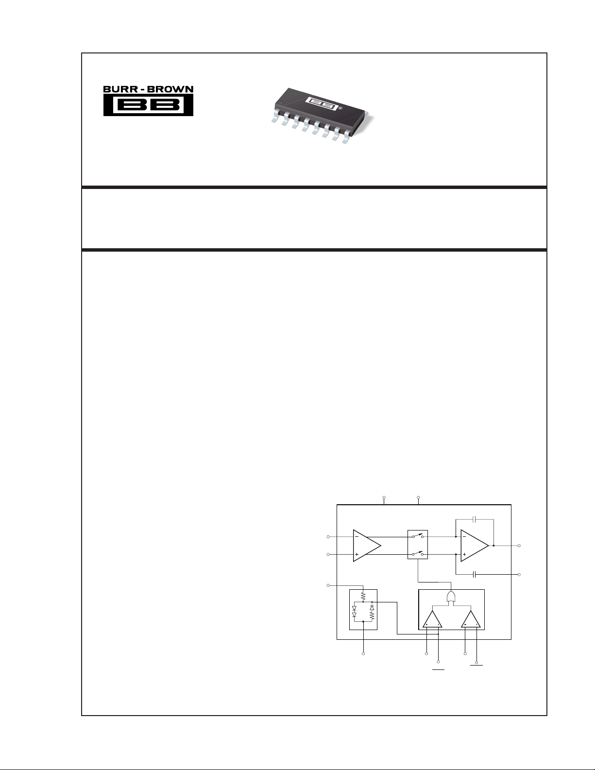
The SHC605 is a monolithic high-speed, high accuracy track-and-hold amplifier. It combines fast acquisition and low distortion to provide a complete solution for a wide range of sampling applications. Its new
proprietary closed-loop architecture provides a singlechip solution to many data acquisition problems formerly requiring more than one device. Noninverting,
inverting, and differential gain configurations are easy
to apply with the SHC605. An on-board logic reference circuit makes the SHC605 compatible with both
single-ended and differential ECL or TTL clock inputs. An internal track-mode lockout circuit allows
edge-triggered operation in data acquisition systems.
The SHC605 is available in a SO-16 surface-mount
package specified for the –40C to +85C industrial
temperature range.
–IN
+IN
Select
+V
2, 3 15, 16
8
1
10
–V
S
S
C
1
C
2
9
5, 6, 7
V
out
AGND
412111413
DGND
International Airport Industrial Park • Mailing Address: PO Box 11400 • Tucson, AZ 85734 • Street Address: 6730 S. Tucson Blvd. • Tucson, AZ 85706
Tel: (520) 746-1111 • Twx: 910-952-1111 • Cable: BBRCORP • Telex: 066-6491 • FAX: (520) 889-1510 • Immediate Product Info: (800) 548-6132
©
1992 Burr-Brown Corporation PDS-1165D Printed in U.S.A. July, 1993
Hold
Thresh/
Hold
Lock
Lock
SPECIFICATIONS
ELECTRICAL
At TA = +25°C, ±VS = ±5V, G = +1V/V, RL = 100Ω, CL = 5pF, and ECL Hold/Hold Inputs, unless otherwise noted.
SHC605AU
PARAMETER CONDITION TEMP RANGE MIN TYP MAX UNITS
DC INPUT PARAMETERS
Offset Voltage Full ±1 ±7.5 mV
Power Supply Rejection V
Input Bias Current V
Input Offset Current V
Common-Mode Input Range Full ±2.0 ±2.5 V
Common-Mode Rejection V
Differential Input Impedance Full 13||1 kΩ||pF
Common-Mode Input Impedance Full 2||1 MΩ||pF
Open-Loop Voltage Gain V
OUTPUT
Voltage Output R
Current Output +25°C ±40 ±80 mA
Short Circuit Current Full ±140 mA
Output Resistance,
Closed-Loop: Track-Mode DC Full 0.0001 Ω
Hold-Mode DC Full 0.01 Ω
DIGITAL INPUTS/OUTPUTS
TTL Input Levels
V
IL
V
IH
Single-Ended ECL Input Levels
V
IL
V
IH
Common-Mode Input Voltages Hold/Hold Full –3 +5 V
(1)
(2)
Differential Input Voltages Hold/Hold and Lock/Lock Inputs Full 0.2 5.0 V
Digital Input Currents
I
, Lock/Lock Inputs Only ECL Logic “LO”, VIL = –1.60V Full 5 µA
IL
I
, Hold/Hold Inputs Only ECL or TTL Logic “LO” Full –100 µA
IL
I
, Lock/Lock Inputs Only Logic “HI”, VIH = –1.0V Full 50 µA
IH
I
, Hold/Hold Inputs Only Full –10 µA
IH
Threshold Voltage Output
(4)
TTL
(5)
ECL
(3)
TRACK-MODE RESPONSE
Closed-Loop Bandwidth Gain = +1V/V +25°C 100 200 MHz
Full Power Response ±1V Input, –3dB Output Full 32 MHz
Slew Rate
Acquisition Time to 1%
(6)
(7)
0.1% 2V Step Full 23 35 ns
0.012% 2V Step Full 30 45 ns
0.012% 4V Step Full 40 60 ns
Input Voltage Noise 1MHz to 100MHz 2.5 nV√Hz
Input Bias Current Noise 1MHz to 100MHz 2.5 pA/√Hz
Differential Gain 3.58MHz, V
Differential Phase 3.58MHz, V
Spurious Free Dynamic Range
(5MHz) V
(10MHz) V
NOTE: (1) Select (Pin 10) connected to +VS for TTL threshold voltage on Pin 11. (2) Select (Pin 10) connected to –VS for ECL threshold voltage on Pin 11. (3) Output
voltage on pin 11. (4) Pin 10 (Select) connected to +V
(7) Acquisition time includes hold-to-track delay switch time. (8) Hold noise is proportional to the time in the hold mode. For example, if the hold time is 25ns, the
accumulated noise is 10µVrms. (9) This is the maximum length of time the SHC605 can remain in the hold mode and still maintain a linear droop rate. (10) Select
(Pin 10) connected to +V
.
S
= ±4.5 to ±5.5V +25°C60 85 dB
S
= 0V Full 15 50 µA
CM
= 0V Full ±0.2 ±5 µA
CM
= ±2VDC Full 80 dB
CM
= ±2V, RL = 100Ω +25°C 100 dB
O
= 50Ω Full ±2.0 ±2.5 V
L
Full ±40 ±60 mA
Hold Input Only
Logic “LO” Full 0 +1.0 V
Logic “HI” Full +2.0 +5.0 V
Hold/Hold and Lock/Lock Inputs
Logic “LO” Full –1.80 –1.45 V
Logic “HI” Full –1.05 –0.80 V
Lock/Lock Full –V
S
+3 V
Full 1.1 1.5 1.9 V
–VS = –5.2V Full –1.40 –1.10 V
Gain = +2V/V +25°C 75 MHz
Gain = +5V/V +25°C 20 MHz
Gain = +10V/V +25°C 10 MHz
G = +1, 2V Step +25°C 140 200 V/µs
Full 120 200 V/µs
2V Step Full 15 25 ns
= 0 to 0.7Vp–p 0.005 %
O
= 0 to 0.7Vp–p 0.005 Degrees
O
= ±1V 83 dBc
O
= ±1V 73 dBc
O
. (5) Pin 10 (Select) connected to –VS. (6) Slew rate is rate of change from 10% to 90% of a 2V output step.
S
The information provided herein is believed to be reliable; however, BURR-BROWN assumes no responsibility for inaccuracies or omissions. BURR-BROWN
assumes no responsibility for the use of this information, and all use of such information shall be entirely at the user’s own risk. Prices and specifications are subject
to change without notice. No patent rights or licenses to any of the circuits described herein are implied or granted to any third party. BURR-BROWN does not authorize
or warrant any BURR-BROWN product for use in life support devices and/or systems.
®
SHC605
2
SPECIFICATIONS (CONT)
ELECTRICAL
At TA = +25°C, ±VS = ±5V, G = +1V/V, RL = 100Ω, CL = 5pF, and ECL Hold/Hold Inputs, unless otherwise noted.
SHC605AU
PARAMETER CONDITION TEMP RANGE MIN TYP MAX UNITS
TRACK-TO-HOLD SWITCHING
V
IN
= 0V
Aperture Delay Full 1.7 ns
Aperture Jitter Full 2.4 ps rms
Pedestal Offset +25°C ±5 ±20 mV
over Temperature Full ±5 ±25 mV
Transient Amplitude Full ±5mV
Settling Time to 1mV Full 8 15 ns
100µV Full 15 ns
HOLD-MODE RESPONSE
Spurious Free Dynamic Range
(1MHz, 20MSPS) V
(2MHz, 20MSPS) V
(5MHz, 20MSPS) V
(10MHz, 20MSPS) V
(10MHz, 20MSPS) V
Hold Noise
Droop Rate Full ±1 ±8 mV/µs
Hold Time
(8)
(9)
= ±1V Full 78 90 dBc
O
= ±1V Full 74 86 dBc
O
= ±1V Full 65 77 dBc
O
= ±1V +25°C 60 dBc
O
= ±0.5 +25°C 72 dBc
O
400xt
H
V/s rms
Full 2 µs
Feedthrough Rejection (20MHz) +25°C85dB
POWER SUPPLY
Specified Operating Voltage Full ±4.50 ± 5 ±5.50 V
Positive Supply Current
Negative Supply Current
(10)
(10)
Full 34 39 mA
Full 33 39 mA
Total Power Dissipation Full 335 390 mW
TEMPERATURE RANGE
Specification Ambient Full –40 +85 °C
Storage –55 +150 °C
Thermal Resistance,
NOTE: (1) Select (Pin 10) connected to +V
Output voltage on pin 11. (4) Pin 10 (Select) connected to +V
output step. (7) Acquisition time includes hold-to-track delay switch time. (8) Hold noise is proportional to the time in the hold mode. For example, if the hold time
θ
JA
for TTL threshold voltage on Pin 11. (2) Select (Pin 10) connected to –VS for ECL threshold voltage on Pin 11. (3)
S
. (5) Pin 10 (Select) connected to –VS. (6) Slew rate is rate of change from 10% to 90% of a 2V
S
Full 100 °C/W
is 25ns, the accumulated noise is 10µVrms. (9) This is the maximum length of time the SHC605 can remain in the hold mode and still maintain a linear droop rate.
(10) Select (Pin 10) connected to +V
.
S
®
3
SHC605
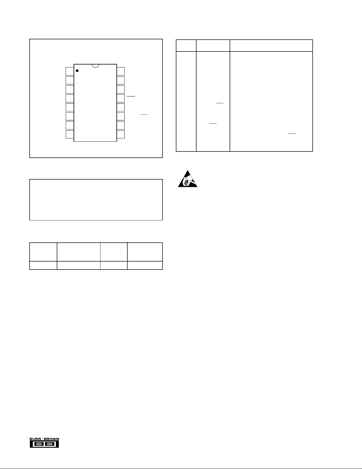
PIN CONFIGURATION PIN DESCRIPTION
PIN # SYMBOL DESCRIPTION
U Package SO-16
1
+In
2
+V
S
3
+V
S
4
DGND
5
AGND
6
AGND
7
AGND
8
–In
16
–V
15
–V
14
Lock
13
Lock
12
Hold
11
Thresh/Hold
10
Select
9
V
S
S
OUT
1 +In Non-Inverting Input
2+V
3+V
4 DGND Digital Ground
5 AGND Analog Ground
6 AGND Analog Ground
7 AGND Analog Ground
8 –In Inverting Input
9V
10 Select +5V Selects TTL; –5V Selects ECL
11 Thresh/Hold Logic threshold for single-ended
12 Hold True Hold input
13 Lock Complement Lock Input
14 Lock True Lock input; Locks SHC605 in
15 –V
16 –V
S
S
OUT
S
S
+5V Supply
+5V Supply
Output Voltage
operation or complement Hold input for
differential operation
Hold-mode regardless of Hold/Hold Inputs
–5V Supply
–5V Supply
ABSOLUTE MAXIMUM RATINGS
Supply ............................................................................................. ±7VDC
Input Voltage Range ............................................................................ ± 5V
Differential Input Voltage .................... ±5.5V (
Storage Temperature Range ..........................................–40°C to +125°C
Lead Temperature (soldering, SOIC 3s) ....................................... +260°C
Output Short Circuit to Ground (+25°C) ................. Continuous to Ground
Junction Temperture (T
) ............................................................... +175°C
j
between +In and –In inputs
PACKAGE/ORDERING INFORMATION
PACKAGE
DRAWING TEMPERATURE
PRODUCT PACKAGE NUMBER
SHC605AU SO-16 Surface-Mount 265 –40°C to +85°C
NOTE: (1) For detailed drawing and dimension table, please see end of data
sheet, or Appendix D of Burr-Brown IC Data Book.
(1)
RANGE
ELECTROSTATIC
DISCHARGE SENSITIVITY
)
This integrated circuit can be damaged by ESD. Burr-Brown
recommends that all integrated circuits be handled with
appropriate precautions. Failure to observe proper handling
and installation procedures can cause damage.
ESD damage can range from subtle performance degradation to complete device failure. Precision integrated circuits
may be more susceptible to damage because very small
parametric changes could cause the device not to meet its
published specifications.
®
SHC605
4
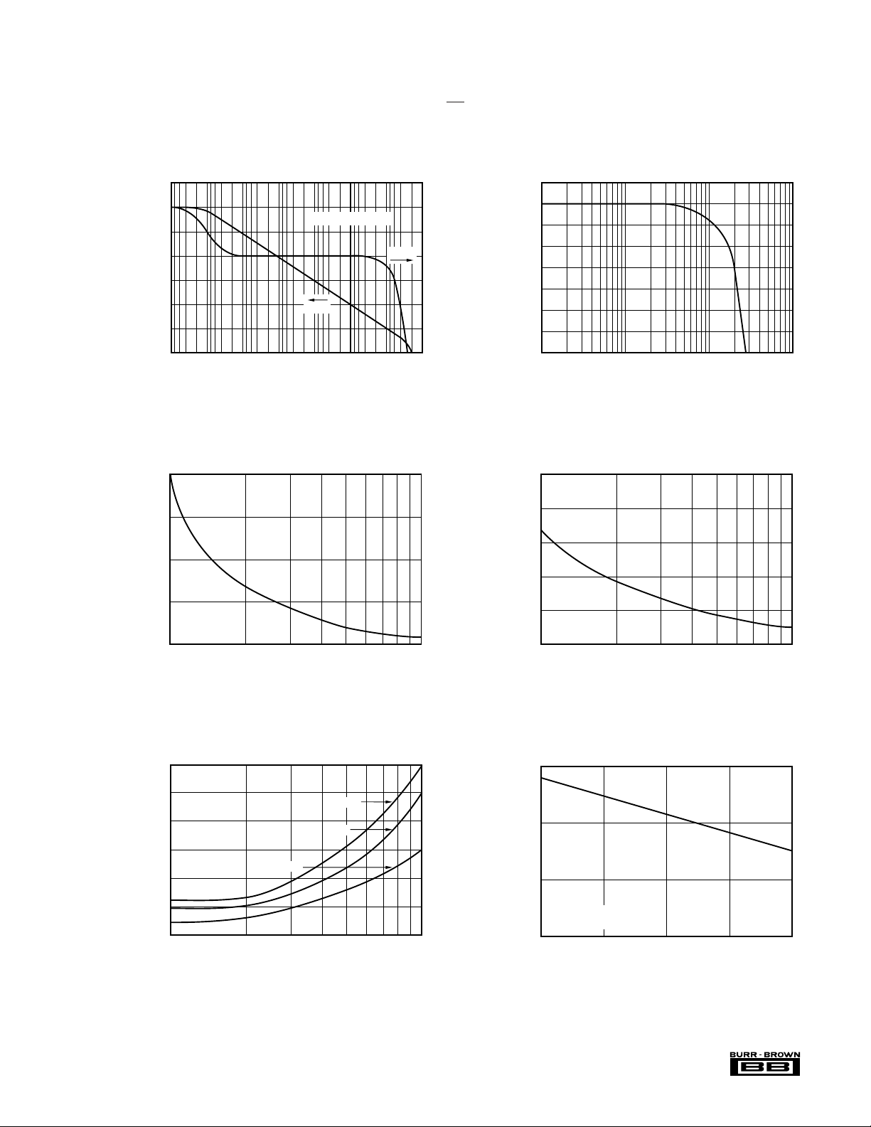
TYPICAL PERFORMANCE CURVES
INVERTING CLOSED-LOOP GAIN
vs SMALL SIGNAL BANDWIDTH
Small Signal Bandwidth (MHz)
Inverting Closed-Loop Gain (V/V)
–1 –2 –5 –10
100
80
60
40
20
0
At TA = +25°C, ±VS = ±5V, G = +1V/V, RL = 100Ω, CL = 5pF, and ECL Hold/Hold Inputs, unless otherwise noted.
OPEN-LOOP FREQUENCY RESPONSE (Track Mode)
120
100
80
60
40
20
Open-Loop Voltage Gain (dB)
0
–20
100 1k 10k 100k 1M 10M 100M 1G
Frequency (Hz)
NON-INVERTING CLOSED-LOOP GAIN
200
150
100
vs SMALL SIGNAL BANDWIDTH
Phase Margin ≈ 65°
Gain
Phase
0
–45
–90
–135
–180
–225
Phase Shift (°)
Gain (dB)
CLOSED-LOOP GAIN = +1V/V
vs FREQUENCY (Track Mode)
0
–1
–2
–3
–4
–5
–6
–7
1 10 100 1000
Frequency (MHz)
50
Small Signal Bandwidth (MHz)
0
+1 +2 +5 +10
Non-Inverting Closed-Loop Gain (V/V)
150
125
100
75
50
Acquisition Time (ns)
25
0
vs NON-INVERTING CLOSED-LOOP GAIN
+1 +2 +5 +10
ACQUISITION TIME
0.01%
0.1%
1%
Inverting Closed-Loop Gain (V/V)
75
70
SNR (dB)
65
V
OUT
60
DC 2.5 5 7.5 10
SNR vs INPUT FREQUENCY
= 2.0Vpp
20MSPS
Input Frequency (MHz)
®
5
SHC605

TYPICAL PERFORMANCE CURVES (CONT)
At TA = +25°C, ±VS = ±5V, G = +1V/V, RL = 100Ω, CL = 5pF, and ECL Hold/Hold Inputs, unless otherwise noted.
LARGEST HARMONIC
100
95
90
85
SFDR (dB)
80
75
70
DC246810
100
90
80
vs INPUT FREQUENCY (Track Mode)
Gain = +1
Gain = +2
Input Frequency (MHz)
FEEDTHROUGH REJECTION
vs INPUT FREQUENCY
V
OUT
= 2.0Vpp
LARGEST HARMONIC
90
85
80
75
SFDR (dB)
70
65
60
DC246810
120
100
80
vs INPUT FREQUENCY (Hold Mode)
V
= 2.0Vpp
O
20MSPS
Input Frequency (MHz)
POWER SUPPLY REJECTION
vs SUPPLY RIPPLE FREQUENCY (Track Mode)
70
60
Feedthrough Rejection (dB)
50
10 20 40 60 100 200
Input Frequency (MHz)
2.5
2.0
|
1.5
1.0
Droop Rate (mV/µs)
|
0.5
0
–50 –25 0 25 50 75 100
DROOP RATE vs TEMPERATURE
Temperature (°C)
60
40
Power Supply Rejection (dB)
20
100 1000 10k 100k 1M 10M 100M
Frequency (Hz)
0
2
4
6
Pedestal (mV)
8
10
–50 –25 0 25 50 75 100
PEDESTAL vs TEMPERATURE
Temperature (°C)
®
SHC605
6

TYPICAL PERFORMANCE CURVES (CONT)
HOLD-MODE DISTORTION
AT 20MSPS, V
IN
= 5MHz
Amplitude (dB)
Frequency (MHz)
0
0
–20
–40
–60
–80
–100
–120
16 32 48 64
V
OUT
= 2Vpp
R
L
= 100Ω
V
IN
= 5MHz
f
T/H
= 20MHz
t
TRACK
= 35ns
HOLD-MODE DISTORTION
AT 20MSPS, V
IN
= 10MHz
Amplitude (dB)
Frequency (MHz)
0
0
–20
–40
–60
–80
–100
–120
16 32 48 64
V
OUT
= 2Vpp
R
L
= 100Ω
V
IN
= 10MHz
f
T/H
= 20MHz
t
TRACK
= 35ns
At TA = +25°C, ±VS = ±5V, G = +1V/V, RL = 100Ω, CL = 5pF, and ECL Hold/Hold Inputs, unless otherwise noted.
0
–20
–40
–60
Amplitude (dB)
–80
–100
–120
0
0
–20
–40
–60
Amplitude (dB)
–80
HOLD-MODE DISTORTION
AT 20MSPS, V
= 2MHz
IN
V
= 2Vpp
OUT
= 100Ω
R
L
= 2MHz
V
IN
= 20MHz
f
T/H
= 35ns
t
TRACK
2nd
51015
Frequency (MHz)
HOLD-MODE DISTORTION
3rd
= 10MHz
IN
V
OUT
= 100Ω
R
L
= 10MHz
V
IN
= 20MHz
f
T/H
t
TRACK
= 1Vpp
= 35ns
AT 20MSPS, V
2nd
2nd
3rd
2nd 3rd
–100
–120
0
16 32 48 64
Frequency (MHz)
®
7
SHC605

TIMING DEFINITIONS
Acquisition Time is the time it takes to reacquire the input
signal when switching from the hold to track mode. This
time interval starts at 50% of the clock transition and ends
when the input signal is reacquired to within a specified
accuracy at the output. This specification does not include
the track-to-hold settling time.
Aperture Delay is a measure of the track-to-hold switch
delay time. It is the difference between the analog input
amplifier’s signal path delay and the digital track-to-hold
switch delay. A positive delay indicates the digital switch
delay is larger than the analog amplifier delay.
Aperture Jitter is random variation in the aperture delay.
This specification is measured in ps-rms and results in phase
noise on the held signal. A large aperture jitter value can
manifest itself by degrading the SNR of a sampling ADC.
Droop Rate is the change of the held output voltage as a
function of time. The measurement starts immediately after
the device switches from the track to hold mode.
Feedthrough Rejection is a measure of the amount of the
input signal that “feeds through” to the output while the
device is in the hold mode. This specification is usually a
function of frequency, with degradation at higher frequencies.
Hold-to-Track Delay is the time from the track command
to the point when the output begins changing to acquire a
new signal. This delay is included in the SHC605’s specified
acquisition time.
Pedestal Offset is the error voltage step incurred at the
output when the device is switched from the track to hold
mode.
Track-to-Hold Settling Time is the time for the track to
hold transient to settle to within a specified accuracy.
Analog
Input
Analog
Output
Hold
Command
+2V
–2V
+2V
–2V
0V
0V
“1”
Aperture
Delay
Voltage
Level Held
Acquisition Time
Hold to
Track
Switch
Delay
Time
“Hold” “Track” “Hold”
Track to
Hold Settling
“0”
FIGURE 1. SHC605 Timing Diagram.
®
SHC605
8

THEORY OF OPERATION
The SHC605 is a monolithic track-and-hold circuit fabricated on an extremely fast complementary bipolar process.
Figure 2 provides a simplified circuit diagram of the SHC605.
A conventional two-stage operational amplifier is shown
with a standard differential phase compensation scheme
sometimes referred to as “doublet compensation.” Capacitors C1 and C2 compensate the amplifier in the track-mode
and hold the analog output signal in the hold-mode. Switching from track to hold is achieved by turning off the
amplifier’s input stage and isolating C
and C2 from the
1
input signal.
The differential two-stage amplifier architecture of the
SHC605 provides many performance advantages over traditional open-loop designs. The use of differential hold capacitors provides a first-order correction for many errors
including distortion, pedestal, and droop. A dominant cause
of distortion in high-speed amplifiers is the nonlinear transistor junction capacitance connected to the hold capacitor(s).
This parasitic capacitance varies as the voltage across it
changes. Most open-loop track-and-hold circuits have a
fixed gain of +1V/V, which means the hold capacitor(s) and
parasitic junction capacitance sees the full output signal
swing. In the SHC605 the second gain stage attenuates the
signal across the capacitors and greatly reduces the nonlinear capacitance. The SHC605’s second stage has a unitygain bandwidth of approximately 250MHz and its open-loop
gain rolls off at –20dB/decade. With a 2.5MHz signal, the
voltage across the hold capacitors is 100 times less than the
output signal, and therefore, the nonlinear capacitance is
greatly reduced.
The SHC605’s patented architecture provides users with an
extremely accurate high-speed operational track-and-hold
amplifier. All common operational amplifier transfer functions can be realized with the SHC605; i.e. unity-gain, noninverting gain, inverting gain, and differential gain. These
configurations are shown in Figures 3 through 6. In many
instances, the SHC605 provides a superior single-chip solution to applications previously requiring two or more devices. As with any conventional voltage feedback op amp, it
is important to consider tradeoffs between noise, bandwidth,
and settling time for these applications. Refer to Discussion
of Performance and Typical Performance Curves for more
details.
+V
S
C
2
C
Track/Hold
+In
–In
FIGURE 2. SHC605 Simplified Circuit Diagram.
C
Comp
1
G = 1 V
OUT
C
1
2
C
3
–V
S
®
9
SHC605

DISCUSSION OF
PERFORMANCE
DISTORTION
Hold-mode distortion is an important specification for a
track-and-hold amplifier. This is a measure of the accuracy
of the amplifier’s held output while sampling a sinusoidal
input signal. It includes errors from both the switching
network and the amplifier’s signal path. Hold-mode distortion depends on the input signal’s amplitude and frequency
as well as the sampling rate. The biggest cause of distortion
in the SHC605 is slew-induced nonlinearity; the higher the
amplitude of a high frequency input, the higher the distortion. Hold-mode distortion can also result from sampling too
fast or not allowing enough acquisition time or track-to-hold
settling time. The SHC605 has a typical 0.01% acquisition
time of 30ns for a 2V step, and a typical 100µV track-tohold settling time of 15ns. Thus, for 12-bit accuracy the
clock rate should not exceed 22MHz (refer to Typical
Performance Curves for details).
NOISE
The SHC605’s noise performance is almost completely
determined by track-mode noise. This is the noise sampled
by the differential hold capacitors during track-mode, which
is greater than the noise measured directly at the output. The
input referred noise of the SHC605 is 2.5nV/√Hz. For unitygain this corresponds to an output noise of approximately
35µVrms; which is much lower than the typical 150µVrms
noise sampled by the hold capacitors. The track-mode noise
sampled by the hold capacitors is independent of closedloop gain, and therefore, the SHC605 can be used with
higher closed-loop gain without degrading the overall noise
performance.
The SHC605’s noise performance is also affected by hold-
mode noise and aperture jitter. Hold-mode noise is the result
of current noise reacting with the hold capacitors. This noise
accumulates on the capacitors at a rate which is proportional
to the square root of the hold time. For sample rates above
1MHz this noise is usually insignificant. Aperture jitter
describes the random variation in track-to-hold aperture
delay, and causes increased hold-mode noise when high
slew rate signals are sampled. A differential ECL clock input
will provide lower aperture jitter than a single-ended ECL or
TTL clock.
CHOOSING THE BEST ARCHITECTURE
The SHC605 is basically a high-speed operational amplifier
which can hold its output on command. Unlike traditional
high-speed track-and-hold amplifiers, which have fixed gains
of +1V/V, the SHC605 can be used with non-inverting,
inverting, or differential gains. In many applications, a
single SHC605 can be used to solve a problem that previously required two or more devices.
Figures 3 through 6 show the SHC605 connected for noninverting, inverting, and differential gains. As with any op
amp, it is important to consider performance tradeoffs for all
of these configurations. For gains less than ±10, the SHC605’s
track-to-hold settling, pedestal offset, droop, and total holdmode noise remains constant. However, small-signal bandwidth and acquisition time will be compromised as the
closed-loop gain is increased (refer to the Typical Performance Curves for details).
+5V
1µF
V
IN
V
IN
.01µF
1
2
3
4
5
6
7
8
+In
+V
S
+V
S
DGND
AGND
AGND
AGND
–In
50Ω
–V
–V
Lock
Lock
Hold
Hold
Select
V
OUT
16
S
15
S
14
13
12
11
10
9
.01µF 1µF
NC
Hold
+5V = TTL
–5V = ECL
V
OUT
–5V
+5V
1µF
.01µF
R
1
+In
2
+V
S
3
+V
S
4
DGND
5
AGND
6
AGND
7
AGND
8
–In
249Ω
2
249Ω
V
OUT
V
IN
R
1
= 1 +
–V
–V
Lock
Lock
Hold
Hold
Select
V
OUT
16
S
15
S
14
13
12
11
10
9
R
1
R
2
.01µF
NC
FIGURE 3. Gain of +1 Track-and-Hold Amplifier. FIGURE 4. Gain of +2 Track-and-Hold Amplifier.
®
SHC605
10
–5V
1µF
Hold
+5V = TTL
–5V = ECL
V
OUT

+5V
+In
+V
S
+V
S
DGND
AGND
AGND
AGND
–In
–V
S
–V
S
Lock
Lock
Hold
Hold
Select
V
OUT
1
2
3
4
5
6
7
8
16
15
14
13
12
11
10
9
1µF
.01µF
.01µF 1µF
–5V
+5V
V
+IN
NC
Hold
+5V = TTL
–5V = ECL
V
OUT
249Ω
249Ω
V
–IN
249Ω
249Ω
V
OUT
R
1
R
2
= (V
+IN
– V
–IN
)
R
1
R
2
R
2
R
1
1µF
125Ω
1
+In
2
+V
S
.01µF
R
V
IN
249Ω
3
+V
S
4
DGND
5
AGND
6
AGND
7
2
AGND
8
–In
R
249Ω
Lock
Lock
Hold
Hold
Select
V
1
–V
–V
OUT
16
S
15
S
14
13
12
11
10
9
.01µF
NC
–5V
1µF
Hold
+5V = TTL
–5V = ECL
V
OUT
V
OUT
V
R
1
= –
R
IN
2
FIGURE 5. Gain of –1 Track-and-Hold Amplifier. FIGURE 6. Differential Gain of 1 Track-and-Hold Amplifier.
APPLICATIONS INFORMATION
LOGIC COMPATIBILITY/TRACK-TO-HOLD
SWITCHING
The SHC605 contains an internal reference circuit which
produces either an ECL or TTL logic threshold voltage for
single-ended track-to-hold switching. Differential ECL
switching is also possible with the SHC605. Table I provides
the proper pin connections for all of the possible switching
options and the Performance Specifications Table gives the
logic levels and input bias currents.
LOCKOUT CIRCUITRY
The SHC605 includes additional logic circuitry which allows edge-triggered operation for sampling ADCs. The
lockout comparator and Track/Hold comparator form a wiredor mode control circuit as shown in the block diagram on
page one. When the Lock input, pin 14, is high with respect
to the Lock input, pin 13, the SHC605 is in the Hold-mode
regardless of the Hold/Hold inputs. This feature provides
more flexibility in the convert command duty cycle and
reduces noise resulting from aperture jitter.
Figure 7 shows how the SHC605 lockout circuit can be used
with an ECL one-shot to provide an edge-triggered sampling
LOGIC TYPE (Pin 4) (Pin 10) (Pin 11) (Pin 12)
Single-ended TTL GND +5V NC Clock
Single-ended ECL GND –5V NC Clock
Differential ECL NC NC Clock Clock
DGND SELECT THRESH/HOLD HOLD
TABLE I. Track-to-Hold Switching Options.
V
IN
+5V
1µF
FIGURE 7. Edge-Triggered ADC.
.01µF
1
+In
2
+V
S
3
+V
S
4
DGND
5
AGND
6
AGND
7
AGND
8
–In
50Ω
Select
–V
–V
Lock
Lock
Hold
Hold
V
OUT
16
S
15
S
14
13
12
11
10
9
.01µF
V
OUT
ADC. An ECL threshold voltage is generated on Thresh/
Hold (Pin 11), which is connected to Lock (Pin 13), to allow
a single-ended lockout input on Lock (Pin 14). The ECL
convert command is applied directly to the SHC605. The
10ns delay on the ADCs convert signal is to allow for
SHC605 track-to-hold settling. The one-shot’s duty cycle
ECL Convert Command
1µF
–5V
(10ns minimum pulsewidth)
ECL
One-Shot
11
10ns
Delay
Line
Convert
ADC
HOLD LOCK MODE
0 0 Track
0 1 Hold
1 0 Hold
1 1 Hold
Digital
Output
SHC605
®

will depend on the ADC conversion time. In this application
the one-shot is used to set the critical ADC timing which
means the user has more freedom in selecting the convert
command duty cycle. Since the convert command is applied
directly to the SHC605—instead of after additional logic
and clock conditioning—aperture jitter noise is minimized.
OFFSET VOLTAGE ADJUSTMENT
The SHC605’s input offset voltage is laser-trimmed and will
require no further adjustment for most applications. However, if additional adjustment is needed, the circuit in Figure
8 can be used without degrading offset drift with temperature. Avoid external adjustment whenever possible since
extraneous noise, such as power supply noise, can be inadvertently coupled into the amplifier’s inverting input. Remember that additional offset errors can be created by the
amplifier’s input bias currents. Whenever possible, match
the impedance seen by both inputs as is shown with R
. This
3
will reduce input offset voltage errors due to the amplifier’s
input offset current, which is typically only 0.2µA.
20kΩ
+V
–V
CC
R
TRIM
47kΩ
CC
R
1
R3 = R1 || R
8
1
R
SHC605
2
2
9
(1)
damage can cause subtle changes in SHC605 input characteristics without necessarily destroying the device. In precision track-and-hold amplifiers, this may cause a noticeable
degradation in performance. Therefore, static protection is
recommended when handling the SHC605.
+V
CC
ESD Protection Diodes Internally
Connected to All Pins
External
Pin
–V
CC
Internal
Circuitry
FIGURE 9. Internal ESD Protection.
LAYOUT AND BYPASSING
For best performance, good high speed design techniques
must be applied. The component (top) side ground plane
should be as large as possible and continuous (not fragmented). Two ounce copper cladding is recommended.
All traces should be as short as possible, especially the
output. As much of the ground plane as possible should be
removed from around the +In, –In, and V
pins to reduce
OUT
parasitic capacitance and minimize coupling onto the analog
signal path.
Power supply decoupling capacitors must be used as shown
in Figures 3 through 6. The 0.01µF capacitors should be low
inductance surface mount devices and should be connected
as close to the SHC605 ±Vs leads as possible (within 30
mils). The 1µF low frequency bypass capacitors should be
tantalum capacitors (preferably surface mount) and should
be located within one inch of the SHC605. Surface mount
resistors are also recommended and should be placed as
close to the SHC605 as possible to minimize inductance.
VIN or Ground
R
Output Trim Range ≈ +VCC to –V
NOTE: (1) R3 is optional and can be used to cancel
offset errors due to input bias currents.
2
R
TRIM
R
2
CC
R
TRIM
FIGURE 8. Offset Voltage Trim.
INPUT PROTECTION
The SHC605 incorporates on-chip ESD protection diodes as
shown in Figure 9. All pins on the SHC605 are internally
protected from ESD by means of a pair of back-to-back
reverse-biased diodes to either power supply as shown.
These diodes will begin to conduct when the input voltage
exceeds either power supply by about 0.7V. This situation
can occur with loss of the amplifier’s power supplies while
a signal source is still present. The diodes can typically
withstand a continuous current of 30mA without destruction. To insure long term reliability diode current should be
externally limited to 10mA or so whenever possible. Static
®
SHC605
CAPACITIVE LOADS
The SHC605’s output stage has been optimized to drive
resistive loads as low as 50Ω. Capacitive loads will decrease
the amplifier’s phase margin which may cause high frequency peaking or oscillations. Capacitive loads greater than
10pF should be buffered by connecting a small resistance,
usually 20Ω to 50Ω, in series with the output as shown in
(R
is typically 20Ω to 50Ω)
8
SHC605
1
S
R
S
9
R
L
FIGURE 10. Driving Capacitance Load.
12
C
L

Figure 10. This is particularly important when driving high
capacitance loads such as flash A/D converters.
The series resistor, R
SHC605 as possible. If R
, should be connected as close to the
S
causes excessive output attenua-
S
tion, add closed-loop gain to the SHC605 as shown in
Figures 4 through 6.
In general, capacitive loads should be minimized for optimum high frequency performance. Coax lines can be driven
if the cable is properly terminated. The capacitance of
coaxial cable (29pF/foot for RG-58) will not load the amplifier when the coaxial cable or transmission line is terminated
in its characteristic impedance.
APPLICATIONS
The SHC605’s combination of high speed and accuracy,
small size, and low price makes it ideally suited for many
data acquisition applications. Its versatile operational amplifier architecture and switching flexibility provides users
with an extremely reliable single-chip solution to problems
that previously required several components. Figures 11
through 16 show many application circuits using the SHC605.
These include high-speed flash and sub-ranging ADC driving, multi-channel simultaneous sampling, DAC deglitching,
and peak detecting.
Analog
Sampling
FIGURE 11. Sampling ADC.
Analog Input
Ch 1
Ch 2
Ch 3
Ch 4
Input
Clock
Analog
MUX
SHC605
Channel
Select
Hold
Timing
Circuit
SHC605
High-speed Sub-ranging
Hold
or Flash
ADC
Convert
ADC
Digital
Output
Digital
Output
Convert
Sampling
Clock
FIGURE 12. Traditional Data Acquisition System.
Timing
Circuit
13
®
SHC605

Analog Inputs
Ch 1
SHC605
Hold
Ch 2
Ch 3
Ch 4
SHC605
SHC605
SHC605
Hold
Hold
Hold
Analog
MUX
Sampling
Clock
FIGURE 13. Multi-Channel Simultaneous Sampling System.
I Channel
Q Channel
SHC605
Hold
SHC605
Hold
Channel
Select
100Ω
100Ω
–
+
+
–
A
OPA678
B
SHC605
Timing
Circuit
Channel
Select
Hold
ADC
ADC
Convert
Digital
Output
Convert
Digital
Output
Sampling
Clock
FIGURE 14. I/Q Channel Simultaneous Sampling.
®
SHC605
Timing
Circuit
14

Analog
Input
Track
FIGURE 15. High-Speed Peak Detector.
SHC605
Hold
Hold
Input
2µs
max
Output
V
OUT
Comparator
with Hysteresis
Digital
Input
Sampling
Clock
DAC
Intput
DAC
Output
Hold
Track
SHC605
Output
DAC
Convert
011...1
Timing
Circuit
100...0
SHC605
Hold
V
OUT
FIGURE 16. DAC Deglitcher.
15
®
SHC605
 Loading...