

Datasheet SG7812AK, SG7812AR, SG7812AT, SG7805K, SG7805R Datasheet (Microsemi Corporation)
...Page 1
SG7800A/SG7800 SERIES
12/91 Rev 1.3 10/97 LINFINITY Microelectronics Inc.
Copyright 1997 11861 Western Avenue
∞ ∞
∞ ∞
∞ Garden Grove, CA 92841
1 (714) 898-8121
∞∞
∞∞
∞ FAX: (714) 893-2570
POSITIVE FIXED VOLTAGE REGULATOR
The SG7800A/SG7800 series of positive regulators offer self contained,
fixed-voltage capability with up to 1.5A of load current and input voltage up
to 50V (SG7800A series only). These units feature a unique on-chip
trimming system to set the output voltages to within ±1.5% of nominal on the
SG7800A series, ±2.0% on the SG7800 series. The SG7800A versions also
offer much improved line and load regulation characteristics. Utilizing an
improved Bandgap reference design, problems have been eliminated that
are normally associated with the Zener diode references, such as drift in
output voltage and large changes in the line and load regulation.
All protective features of thermal shutdown, current limiting, and safe-area
control have been designed into these units and since these regulators
require only a small output capacitor for satisfactory performance, ease of
application is assured.
Although designed as fixed-voltage regulators, the output voltage can be
increased through the use of a simple voltage divider. The low quiescent
drain current of the device insures good regulation when this method is used.
Product is available in hermetically sealed TO-257, TO-3, TO39 and LCC
packages.
DESCRIPTION FEATURES
••
••
•
Output voltage set internally to
±±
±±
±1.5% on SG7800A
••
••
• Input voltage range to 50V max. on SG7800A
••
••
• Two volt input-output differential
••
••
• Excellent line and load regulation
••
••
• Foldback current limiting
••
••
• Thermal overload protection
••
••
• Voltages available: 5V, 12V, 15V
••
••
• Available in surface mount package
HIGH RELIABILITY FEATURES
- SG7800A/7800
♦♦
♦♦
♦ Available to MIL-STD - 883
♦♦
♦♦
♦ MIL-M38510/10702BXA - JAN7805T
♦♦
♦♦
♦ MIL-M38510/10703BXA - JAN7812T
♦♦
♦♦
♦ MIL-M38510/10704BXA - JAN7815T
♦♦
♦♦
♦ MIL-M38510/10706BYA - JAN7805K
♦♦
♦♦
♦ MIL-M38510/10707BYA - JAN7812K
♦♦
♦♦
♦ MIL-M38510/10708BYA - JAN7815K
♦♦
♦♦
♦ Radiation data available
♦♦
♦♦
♦ LMI level "S" processing available
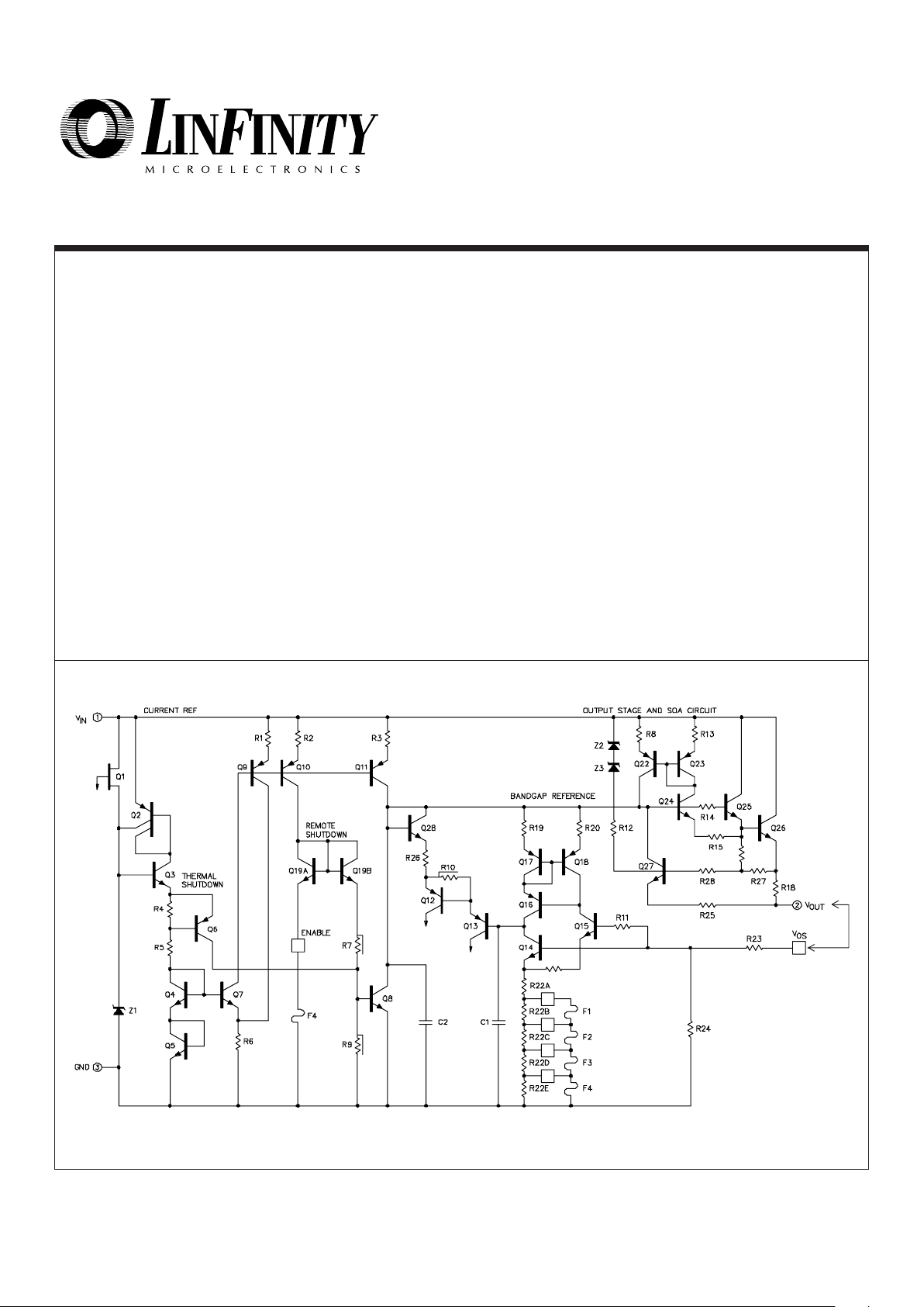
SCHEMATIC DIAGRAM
SG7800A/SG7800
*
* For normal operation the (VOS) sense pin must be externally connected to the load.
Page 2
SG7800A/SG7800 SERIES
12/91 Rev 1.3 10/97 LINFINITY Microelectronics Inc.
Copyright 1997 11861 Western Avenue
∞ ∞
∞ ∞
∞ Garden Grove, CA 92841
2 (714) 898-8121
∞∞
∞∞
∞ FAX: (714) 893-2570
ABSOLUTE MAXIMUM RATINGS (Note 1)
Device Input Voltage Input Voltage Differential
Output Voltage Input Voltage (transient) (Note 3) (Output shorted to ground)
5V 35V 50V 35V
12V 35V 50V 35V
15V 35V 50V 35V
POSITIVE REGULATOR
Operating Junction Temperature
Hermetic (K, T, IG & L - Packages) ......................... 150°C
Storage Temperature Range ..........................
Lead Temperature (Soldering, 10 Seconds) .................
-65°C to 150°C
300°C
Note 1. Values beyond which damage may occur.
THERMAL DATA
K Package:
Thermal Resistance-
Junction to Case, θ
JC
................. 3.0°C/W
Thermal Resistance-
Junction to Ambient, θ
JA
............... 35°C/W
T Package:
Thermal Resistance-
Junction to Case, θ
JC
.................. 15°C/W
Thermal Resistance-
Junction to Ambient, θ
JA
............ 120°C/W
IG Package:
Thermal Resistance-
Junction to Case, θ
JC
................. 3.5°C/W
Thermal Resistance-
Junction to Ambient, θ
JA
.............. 42°C/W
L Package:
Thermal Resistance-
Junction to Case, θ
JC
.................. 35°C/W
Thermal Resistance-
Junction to Ambient, θ
JA
............ 120°C/W
Note A. Junction Temperature Calculation: TJ = TA + (PD x θJA).
Note B. The above numbers for θJC are maximums for the limiting thermal
resistance of the package in a standard mounting configuration.
The θJA numbers are meant to be guidelines for the thermal
performance of the device/pc-board system. All of the above
assume no ambient airflow.
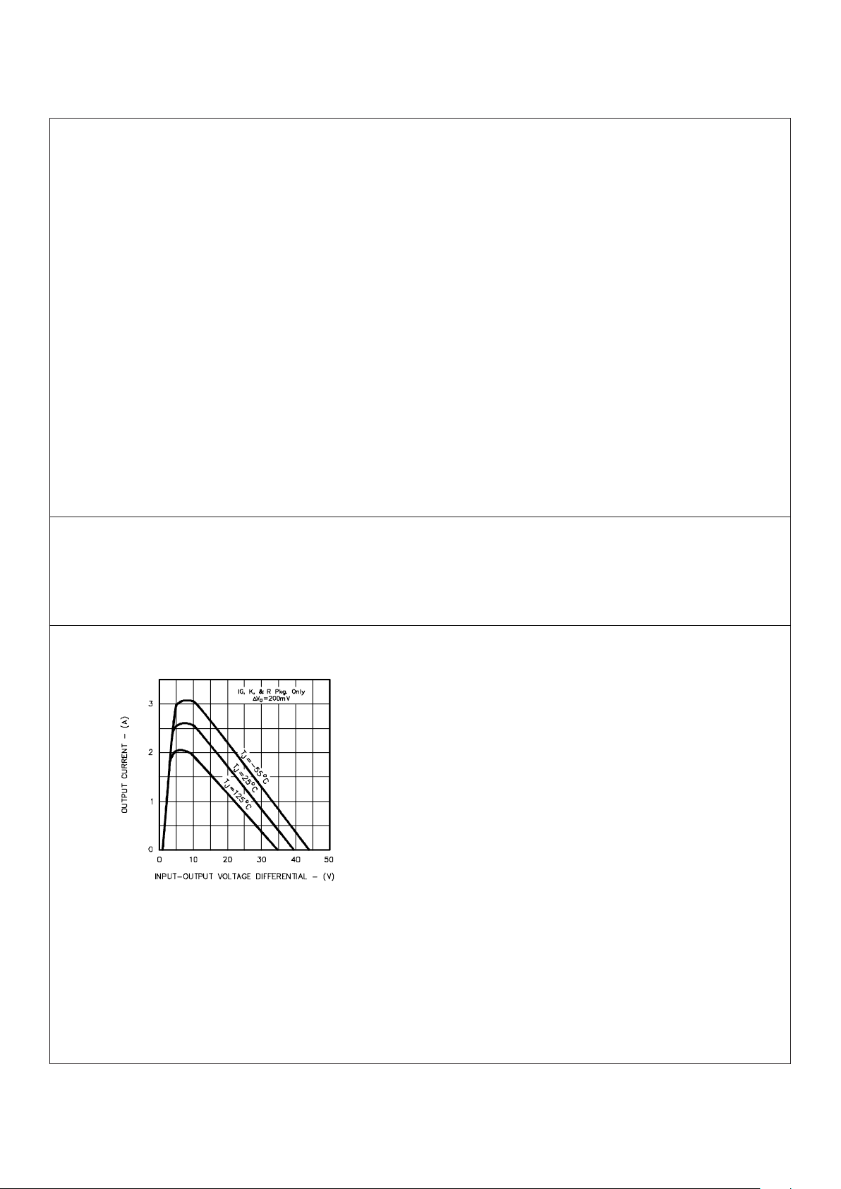
Note 3. Operation at high input voltages is dependent upon load current. When
load current is less than 5mA, output will rise out of regulation as inputoiutput differential icreases beyond 30V. Note also from Figure 1, that
maximum load current is reduced at high voltages. The 50V input rating
of the SG140A series refers to ability to withstnd high line or transient
conditions without damage. Since the regulator's maximum current
capability is reduced, the output may fall out of regulation at high input
voltages under nominal loading.
FIGURE 1.
PEAK OUTPUT CURRENT
VS. INPUT - OUTPUT DIFFERENTIAL
RECOMMENDED OPERATING CONDITIONS (Note 2)
Note 2. Range over which the device is functional.
CHARACTERISTIC CURVES
Operating Junction Temperature Range:
SG7800A/SG7800 ........................................ -55°C to 150°C
Page 3
SG7800A/SG7800 SERIES
12/91 Rev 1.3 10/97 LINFINITY Microelectronics Inc.
Copyright 1997 11861 Western Avenue
∞ ∞
∞ ∞
∞ Garden Grove, CA 92841
3 (714) 898-8121
∞∞
∞∞
∞ FAX: (714) 893-2570
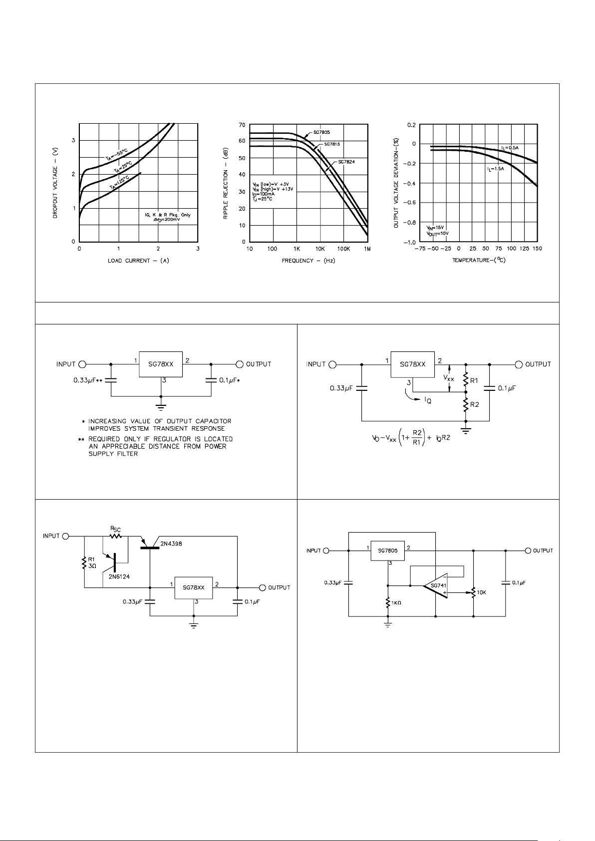
CHARACTERISTIC CURVES (continued)
POSITIVE REGULATOR
FIGURE 2.
MINIMUM INPUT - OUTPUT VOLTAGE
VS. LOAD CURRENT
FIGURE 3.
RIPPLE REJECTION VS. FREQUENCY
FIGURE 4.
TEMPERATURE COEFFICIENT OF OUTPUT VOLTAGE
APPLICATIONS
FIGURE 5 - FIXED OUTPUT REGULATOR FIGURE 6 - CIRCUIT FOR INCREASING OUTPUT VOLTAGE
FIGURE 8 - ADJUSTABLE OUTPUT REGULATOR, 7V to 30V
FIGURE 7 - HIGH OUTPUT CURRENT, SHORT CIRCUIT PROTECTED
Page 4

SG7800A/SG7800 SERIES
12/91 Rev 1.3 10/97 LINFINITY Microelectronics Inc.
Copyright 1997 11861 Western Avenue
∞ ∞
∞ ∞
∞ Garden Grove, CA 92841
4 (714) 898-8121
∞∞
∞∞
∞ FAX: (714) 893-2570
ELECTRICAL SPECIFICATIONS (Note 1)
(Unless otherwise specified, these specifications apply over the operating ambient temperatures for SG7805A/SG7805 with -55°C ≤ TA ≤ 150°C,
VIN = 10V, IO = 500mA for the K and IG -Power Packages-, IO = 100mA for the T and L packages, CIN = 0.33µF, and C
OUT
= 0.1µF. Low duty cycle pulse
testing techniques are used which maintains junction and case temperatures equal to the ambient temperature.)
5.0V POSITIVE REGULATOR
SG7805A/SG7805
Units
SG7805
Min. Typ. Max.Min. Typ. Max.
SG7805A
V
mV
mV
mV
mV
mV
V
V
mA
mA
mA
mA
mA
V
A
A
A
A
dB
µV/V
mV
°C
5.00
5
2
15
5
20
5.00
5.00
4
2
2.0
1.0
20
175
5.20
50
25
50
25
25
5.35
5.35
7
6
0.8
0.5
0.5
2.5
3.3
2.0
1.2
0.7
40
Output Voltage
Line Regulation
(Note 1)
Load Regulation (Note 1)
Total Output Voltage
Tolerance
Quiescent Current
Quiescent Current Change
Dropout Voltage
Peak Output Current
Short Circuit Current
Ripple Rejection
Output Noise Voltage (rms)
Long Term Stability
Thermal Shutdown
4.80
4.65
4.65
1.5
0.5
68
Parameter Test Conditions
TJ = 25°C
V
IN
= 7.5V to 20V, TJ = 25°C
V
IN
= 8V to 12V, TJ = 25°C
Power Pkgs: I
O
= 5mA to 1.5A, TJ = 25°C
I
O
= 250mA to 750mA, TJ = 25°C
T - Pkg: I
O
= 5mA to 500mA, TJ = 25°C
V
IN
=8V to 20V
Power Pkgs: I
O
= 5mA to 1.0A, P ≤ 20W
T - Pkg: I
O
= 5mA to 500mA, P ≤ 2W
Over Temperature Range
T
J
= 25°C
With Line: V
IN
= 8V to 25V
With Load: I
O
= 5mA to 1.0A (Power Pkgs.)
I
O
= 5mA to 500mA (T)
∆V
O
= 100mV, TJ = 25°C
Power Pkgs: I
O
= 1.0A, T - Pkg: IO = 500mA
Power Pkgs: V
IN
= 10V, TJ = 25°C
T - Pkg: V
IN
= 10V, TJ = 25°C
Power Pkgs: V
IN
= 35V, TJ = 25°C
T - Pkg: V
IN
= 35V, TJ = 25°C
∆V
IN
= 10V, f = 120Hz, TJ = 25°C
f = 10Hz to 100KHz
(Note 2)
1000hrs. at TJ = 125°C
I
O
= 5mA
5.00
5
2
15
5
5
5.00
5.00
4
2
2.0
1.0
20
175
5.08
25
12
50
25
25
5.15
5.15
7
6
0.8
0.5
0.5
2.5
3.3
2.0
1.2
0.7
40
4.92
4.85
4.85
1.5
0.5
68
Note 1. All regulation tests are made at constant junction temperature with low duty cycle testing.
2. This test is guaranteed but is not tested in production.
Page 5

SG7800A/SG7800 SERIES
12/91 Rev 1.3 10/97 LINFINITY Microelectronics Inc.
Copyright 1997 11861 Western Avenue
∞ ∞
∞ ∞
∞ Garden Grove, CA 92841
5 (714) 898-8121
∞∞
∞∞
∞ FAX: (714) 893-2570
12V POSITIVE REGULATOR
ELECTRICAL SPECIFICATIONS (Note 1)
(Unless otherwise specified, these specifications apply over the operating ambient temperatures for SG7812A/SG7812 with -55°C ≤ TA ≤ 150°C,
VIN = 19V, IO = 500mA for the K and IG -Power Packages-, IO = 100mA for the T and L packages, CIN = 0.33µF, and C
OUT
= 0.1µF. Low duty cycle pulse
testing techniques are used which maintains junction and case temperatures equal to the ambient temperature.)
SG7812A/SG7812
Units
SG7812
Min. Typ. Max.
Min. Typ. Max.
SG7812A
Test ConditionsParameter
T
J
= 25°C
V
IN
= 14.5V to 30V, TJ = 25°C
V
IN
= 16V to 22V, TJ = 25°C
Power Pkgs: I
O
= 5mA to 1.5A, TJ = 25°C
I
O
= 250mA to 750mA, TJ = 25°C
T - Pkg: I
O
= 5mA to 500mA, TJ = 25°C
V
IN
= 15.5V to 27V
Power Pkgs: I
O
= 5mA to 1.0A, P ≤ 20W
T - Pkg: I
O
= 5mA to 500mA, P ≤ 2W
Over Temperature Range
T
J
= 25°C
With Line: V
IN
= 15V to 30V
With Load:I
O
= 5mA to 1.0A (Power Pkgs.)
I
O
= 5mA to 500mA (T)
∆V
O
= 100mV, TJ = 25°C
Power Pkgs: I
O
= 1.0A, T - Pkg: IO = 500mA
Power Pkgs: T
J
= 25°C
T - Pkg: T
J
= 25°C
Power Pkgs: V
IN
= 35V, TJ = 25°C
T - Pkg: V
IN
= 35V, TJ = 25°C
∆V
IN
= 10V, f = 120Hz, TJ = 25°C
f = 10Hz to 100KHz
(Note 2)
1000hrs. at TJ = 125°C
I
O
= 5mA
Output Voltage
Line Regulation
(Note 1)
Load Regulation (Note 1)
Total Output Voltage
Tolerance
Quiescent Current
Quiescent Current Change
Dropout Voltage
Peak Output Current
Short Circuit Current
Ripple Rejection
Output Noise Voltage (rms)
Long Term Stability
Thermal Shutdown
11.8
11.7
11.7
1.5
0.5
61
12.0
12
6
28
10
10
12.0
12.0
4
2
2.0
1.0
48
175
12.2
60
30
80
40
40
12.3
12.3
7
6
0.8
0.5
0.5
2.5
3.3
1.7
1.2
0.7
40
11.5
11.4
11.4
1.5
0.5
61
12.0
12
6
28
10
10
12.0
12.0
4
2
2.0
1.0
48
175
12.5
120
60
120
60
60
12.6
12.6
7
6
0.8
0.5
0.5
2.5
3.3
1.7
1.2
0.7
40
V
mV
mV
mV
mV
mV
V
V
mA
mA
mA
mA
mA
V
A
A
A
A
dB
µV/V
mV
°C
Note 1. All regulation tests are made at constant junction temperature with low duty cycle testing.
2. This test is guaranteed but is not tested in production.
Page 6

SG7800A/SG7800 SERIES
12/91 Rev 1.3 10/97 LINFINITY Microelectronics Inc.
Copyright 1997 11861 Western Avenue
∞ ∞
∞ ∞
∞ Garden Grove, CA 92841
6 (714) 898-8121
∞∞
∞∞
∞ FAX: (714) 893-2570
15V POSITIVE REGULATOR
ELECTRICAL SPECIFICATIONS (Note 1)
(Unless otherwise specified, these specifications apply over the operating ambient temperatures for SG7815A/SG7815 with -55°C ≤ TA ≤ 150°C,
VIN = 23V, IO = 500mA for the K and IG -Power Packages-, IO = 100mA for the T and L packages, CIN = 0.33µF, and C
OUT
= 0.1µF. Low duty cycle pulse
testing techniques are used which maintains junction and case temperatures equal to the ambient temperature.)
SG7815A/SG7815
Units
SG7815
Min. Typ. Max.
Min. Typ. Max.
SG7815A
Test ConditionsParameter
T
J
= 25°C
V
IN
= 17.5V to 30V, TJ = 25°C
V
IN
= 20V to 26V, TJ = 25°C
Power Pkgs: I
O
= 5mA to 1.5A, TJ = 25°C
I
O
= 250mA to 750mA, TJ = 25°C
T - Pkg: I
O
= 5mA to 500mA, TJ = 25°C
V
IN
= 18.5V to 30V
Power Pkgs: I
O
= 5mA to 1.0A, P ≤ 20W
T - Pkg: I
O
= 5mA to 500mA, P ≤ 2W
Over Temperature Range
T
J
= 25°C
With Line: V
IN
= 18.5V to 30V
With Load:I
O
= 5mA to 1.0A (Power Pkgs.)
I
O
= 5mA to 500mA (T)
∆V
O
= 100mV, TJ = 25°C
Power Pkgs: I
O
= 1.0A, T - Pkg: IO = 500mA
Power Pkgs: T
J
= 25°C
T - Pkg: T
J
= 25°C
Power Pkgs: V
IN
= 35V, TJ = 25°C
T - Pkg: V
IN
= 35V, TJ = 25°C
∆V
IN
= 10V, f = 120Hz, TJ = 25°C
f = 10Hz to 100KHz
(Note 2)
1000hrs. at TJ = 125°C
I
O
= 5mA
Output Voltage
Line Regulation
(Note 1)
Load Regulation (Note 1)
Total Output Voltage
Tolerance
Quiescent Current
Quiescent Current Change
Dropout Voltage
Peak Output Current
Short Circuit Current
Ripple Rejection
Output Noise Voltage (rms)
Long Term Stability
Thermal Shutdown
14.8
14.6
14.6
1.5
0.5
60
15.0
15
8
30
12
12
15.0
15.0
4
2
2.2
0.9
60
175
15.2
75
40
100
50
50
15.4
15.4
7
6
0.8
0.5
0.5
2.5
3.3
1.7
1.2
0.7
40
14.4
14.3
14.3
1.5
0.5
60
15.0
15
8
30
12
12
15.0
15.0
4
2
2.2
0.9
60
175
15.6
150
75
150
75
75
15.7
15.7
7
6
0.8
0.5
0.5
2.5
3.3
1.7
1.2
0.7
40
V
mV
mV
mV
mV
mV
V
V
mA
mA
mA
mA
mA
V
A
A
A
A
dB
µV/V
mV
°C
Note 1. All regulation tests are made at constant junction temperature with low duty cycle testing.
2. This test is guaranteed but is not tested in production.
Page 7

SG7800A/SG7800 SERIES
12/91 Rev 1.3 10/97 LINFINITY Microelectronics Inc.
Copyright 1997 11861 Western Avenue
∞ ∞
∞ ∞
∞ Garden Grove, CA 92841
7 (714) 898-8121
∞∞
∞∞
∞ FAX: (714) 893-2570
CONNECTION DIAGRAMS & ORDERING INFORMATION (See Notes Below)
POSITIVE REGULATOR
Part No.Package
Connection Diagram
3-TERMINAL TO-3
METAL CAN
K-PACKAGE
SG78XXAK/883B -55°C to 125°C
SG7805AK/DESC -55°C to 125°C
SG7812AK/DESC -55°C to 125°C
SG7815AK/DESC -55°C to 125°C
SG78XXAK -55°C to 125°C
SG78XXK/883B -55°C to 125°C
JAN7805K -55°C to 125°C
JAN7812K -55°C to 125°C
JAN7815K -55°C to 125°C
SG78XXK -55°C to 125°C
SG78XXK 0°C to 125°C
Ambient
Temperature Range
Note 1. Contact factory for JAN and DESC product availability.
2. All parts are viewed from the top.
3. "XX" to be replaced by output voltage of specific fixed regulator.
4. Some products will be available in hermetic flat pack (F). Consult factory for price and availability.
5. Both inputs and outputs must be externally connected together at the device terminals.
6. For normal operation, the VO SENSE pin must be externally connected to the load.
3-PIN TO-39 METAL CAN
T-PACKAGE
SG78XXAT/883B -55°C to 125°C
SG7805AT/DESC -55°C to 125°C
SG7812AT/DESC -55°C to 125°C
SG7815AT/DESC -55°C to 125°C
SG78XXAT -55°C to 125°C
SG78XXT/883B -55°C to 125°C
JAN7805T -55°C to 125°C
JAN7812T -55°C to 125°C
JAN7815T -55°C to 125°C
SG78XXT -55°C to 125°C
3-PIN HERMETIC TO-257
IG-PACKAGE (Isolated)
SG78XXAIG/883B -55°C to 125°C
SG7805AIG/DESC -55°C to 125°C
SG7812AIG/DESC -55°C to 125°C
SG7815AIG/DESC -55°C to 125°C
SG78XXAIG -55°C to 125°C
SG78XXIG/883B -55°C to 125°C
SG78XXIG -55°C to 125°C
V
OUT
Tab is GND
GROUND
V
IN
2
1
CASE IS GROUND
V
OUT
V
IN
V
OUT
V
IN
32
GROUND
1
CASE IS GROUND
20-PIN CERAMIC
LEADLESS CHIP CARRIER
L- PACKAGE
SG7805AL/DESC -55°C to 125°C
SG7812AL/DESC -55°C to 125°C
SG7815AL/DESC -55°C to 125°C
SG78XXL/883B -55°C to 125°C
4
5
6
7
8
321
14
15
16
17
18
20 19
11. N.C.
12. V
OUT
13. N.C.
14. N.C.
15. V
O
SENSE
16. N.C.
17. V
IN
18. N.C.
19. N.C.
20. N.C.
1. N.C.
2. V
IN
3. N.C.
4. N.C.
5. N.C.
6. N.C.
7. GND
8. N.C.
9. N.C.
10. V
OUT
9 11121310
(See Notes 5 & 6)
 Loading...