

Page 1
SG6846B
Highly Integrated Green-Mode PWM Controller
SG6846B — Highly Integrated Green-Mode PWM Controller
October 2008
Features
Low Startup Current: 8µA
Low Operating Current: 3.7mA
Peak-Current Mode Operation with Cycle-by-cycle
Current Limiting
PWM Frequency Continuously Decreasing with
Burst Mode at Light Loads
V
Over Voltage Protection (OVP)
DD
AC Input Brownout Protection with Hysteresis
Constant Output Power Limit (Full AC Input Range)
Internal Latch Circuit for OVP, OTP, and OCP
(BLSY, BLSZ)
Two-level OCP Delay with 200ms
Programmable PWM Frequency with Frequency
Hopping
OCP Threshold is 2/3 Peak Current Limit
Soft Startup Time: 5ms
Applications
General-purpose switch-mode power supplies and
flyback power converters, including:
Power Adapters
Open-frame SMPS
SMPS with Surge-current Output, such as for
Printers, Scanners, Motor Drivers
Description
The highly integrated PWM controller, SG6846B,
provides several features to enhance the performance
of fly-back converters. To minimize standby power
consumption, a proprietary green-mode function
provides off-time modulation to continuously decrease
the switching frequency under light-load conditions.
Under zero-load conditions, the power supply enters
burst-mode. This completely shuts off PWM output. If
V
is larger than around 1.6V, PWM pulses out. This
FB
green-mode function enables power supplies to meet
international power conservation requirements.
The SG6846B is designed for SMPS with surge-current
output. It is incorporated with a two-level OCP function.
Besides, the cycle-by-cycle current limiting, if the
switching current is higher than OCP threshold and
lasts for 200ms, SG6846B stops gate immediately and
latches itself (BLSY version) or restarts after V
charges up to 16.5V (BCSY version). SG6846B also
integrates frequency-hopping function internally. The
frequency hopping function helps reduce EMI emission
of a power supply with minimum line filters. It has builtin synchronized slope compensation, proprietary
internal compensation for constant output power limit
over universal AC input range. The gate output is
clamped at 18V to protect the external MOSFET from
over-voltage damage.
Protection include: AC input brownout protection with
hysteresis and V
temperature protection, an external NTC thermistor can
be applied to sense the ambient temperature. When
OCP, V
circuit is used to latch-off the controller. The latch resets
when V
SG6846B is available in 8-pin SOP package.
OVP, or OTP are activated, an internal latch
DD
supply is removed.
DD
over-voltage protection. For over-
DD
DD
Ordering Information
Part
Number
SG6846BLSY -40 to +105°C Yes Green 8-Pin Small Outline Package (SOP) Tape & Reel
SG6846BLSZ -40 to +105°C Yes RoHS 8-Pin Small Outline Package (SOP) Tape & Reel
SG6846BCSY -40 to +105°C No Green 8-Pin Small Outline Package (SOP) Tape & Reel
SG6846BCSZ -40 to +105°C No RoHS 8-Pin Small Outline Package (SOP) Tape & Reel
For Fairchild’s definition of “green” Eco Status, please vis i t : http://www.fairchildsemi.com/company/green/rohs_green.html.
© 2008 Fairchild Semiconductor Corporation www.fairchildsemi.com
SG6846B • Rev. 1.3.4
Operating
Temperature Range
OCP
Latch
Eco
Status
Package
Packing
Method
Page 2
Typical Application
L
AC input
N
EMI
Filter
3
7
VINRIVDD GATE
SG6846B — Highly Integrated Green-Mode PWM Controller
+
+
+
8
+
VO+
VO-
Block Diagram
0.9V/0.7V
VIN
3
7
VDD
4
2
FB
V
DD
-TH-G
UVLO
16.5V/10.5V
6
SENSE
GND
RT
5
1
SG6846B
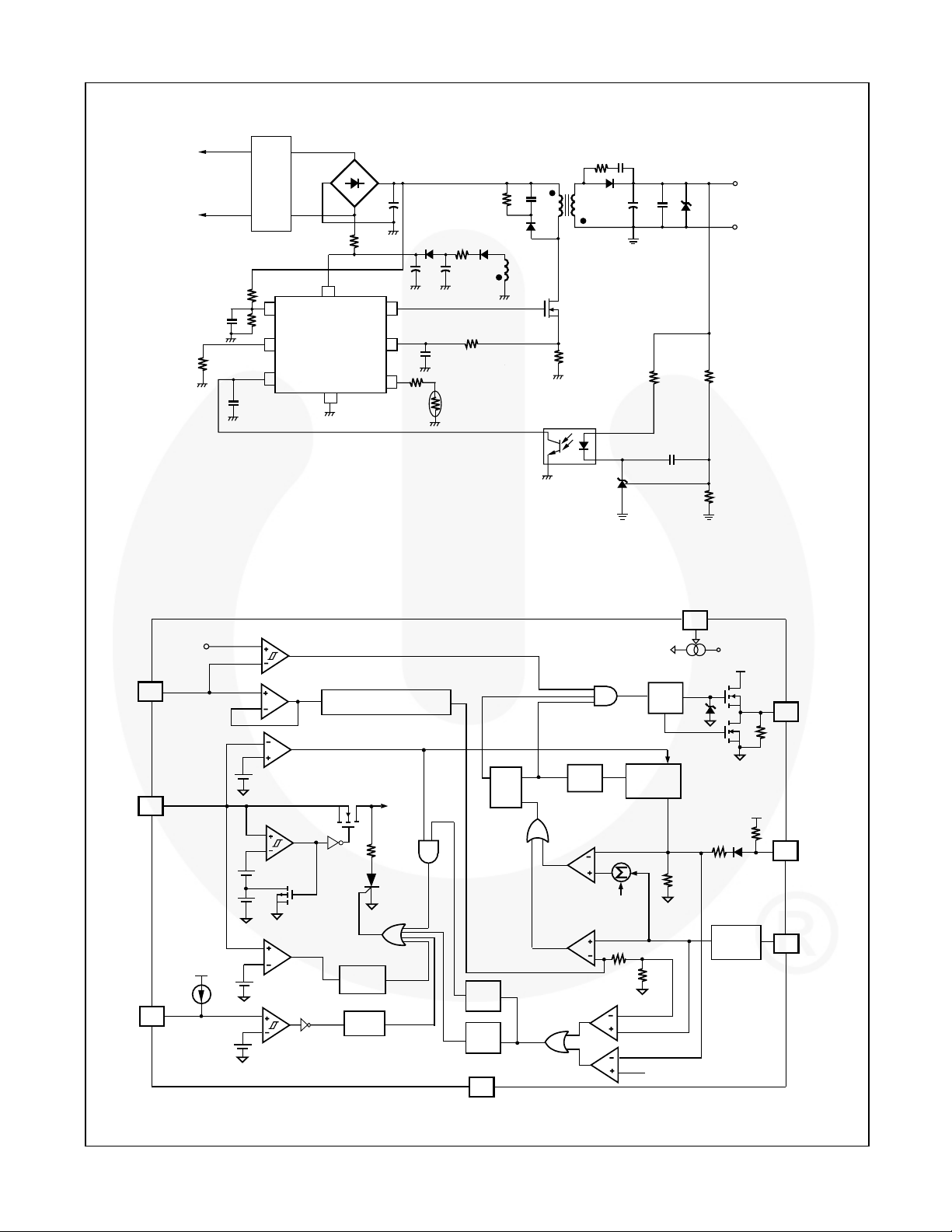
Figure 1. Typical Application
Over Power Compersation
0.895-0.065
Internal
BIAS
Latch
XVIN
4
VDD
Soft
Driver
Slope
1R
Green
Mode
+
3R
1R
Blanking
Circuit
S
Q
R
OSC
Compensation
6.2V
8
2
6
GATE
FB
SENSE
2R
1.15V
RT
23.6V
I
RT
5
1.05V
Debounce
OTP
Delay
SCP
Delay
OCP
Delay
1
GND
Figure 2. Block Diagram
© 2008 Fairchild Semiconductor Corporation www.fairchildsemi.com
SG6846B • Rev. 1.3.4 2
Page 3
Marking Information
SG6846BFTP
XXXXXXXXYWWV
※ Marking for SG6846BLSZ (Pb-free)
SG6846BCSZ (Pb-free)
SG6846B — Highly Integrated Green-Mode PWM Controller
F: L = OCP Latch, C = OCP auto-recovery
T: S = SOP
P: Z = Lead Free + ROHS Compatible
Null = regular package
XXXXXXXX: Wafer Lot
Y: Year; WW: Week
V: Assembly Location
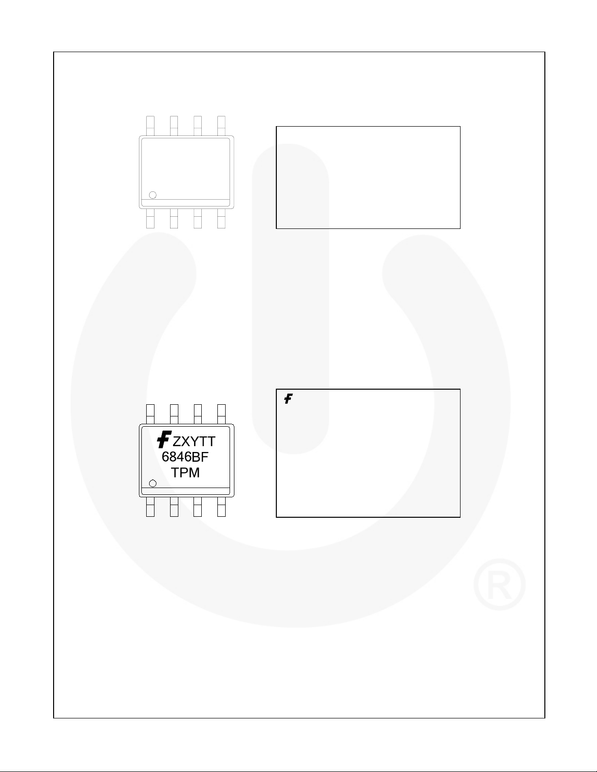
Figure 3. Top Mark 1
: Fairchild logo
Z: Plant Code
X: Year Code
Y: Week Code
TT: Die Run Code
F: L = OCP Latch, C = OCP auto-recovery
T: Package type, S = SOP
Green Package
P: Y =
M: Manufacturing flow code
※ Marking for SG6846BLSY (Green-compound)
SG6846BCSY (Green-compound)
Figure 4. Top Mark 2
© 2008 Fairchild Semiconductor Corporation www.fairchildsemi.com
SG6846B • Rev. 1.3.4 3
Page 4
Pin Configuration
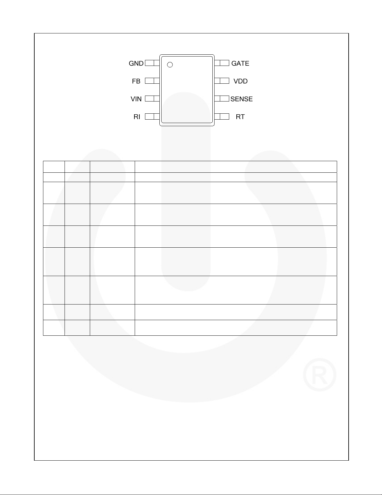
Figure 5. Pin Configuration
Pin Definitions
Pin # Name Function Description
1 GND Ground Ground.
The signal from the external compensation circuit is fed into this pin. The PWM
2 FB Feedback
3 VIN
4 RI
5 RT
6 SENSE Current Sense
7 VDD Power Supply
8 GATE Driver Output
Line-voltage
Detection
Reference
Setting
Temperature
Detection
duty cycle is determined in response to the signal from this pin and the currentsense signal from pin 6.
Line-voltage detection is used for brownout protection with hysteresis. Constant
output power limit over universal AC input range is achieved using this pin. Add
a low-pass filter to filter out line ripple on the bulk capacitor.
A resistor from the RI pin to ground generates a reference current source that
determines the switching frequency. Increasing the resistance reduces the
switching frequency. A 26k resistor results in a 65kHz switching frequency.
For over-temperature protection, an external NTC thermistor is connected from
this pin to the GND pin. The impedance of the NTC decreases at high
temperatures. Once the voltage of the RT pin drops below a threshold, PWM
output is disabled.
The sensed voltage is used for peak-current-mode control and cycle-by-cycle
current limiting. If the switching current is higher than OCP threshold and lasts
for 200ms, SG6846B turns off immediately. This two-level OCP feature is
especially suitable for SMPS with surge current output.
If an open-circuit failure occurs in the feedback loop, the internal protection
circuit disables PWM output as long as V
The totem-pole output driver for the power MOSFET; internally clamped
below 18V.
exceeds a threshold.
DD
SG6846B — Highly Integrated Green-Mode PWM Controller
© 2008 Fairchild Semiconductor Corporation www.fairchildsemi.com
SG6846B • Rev. 1.3.4 4
Page 5
SG6846B — Highly Integrated Green-Mode PWM Controller
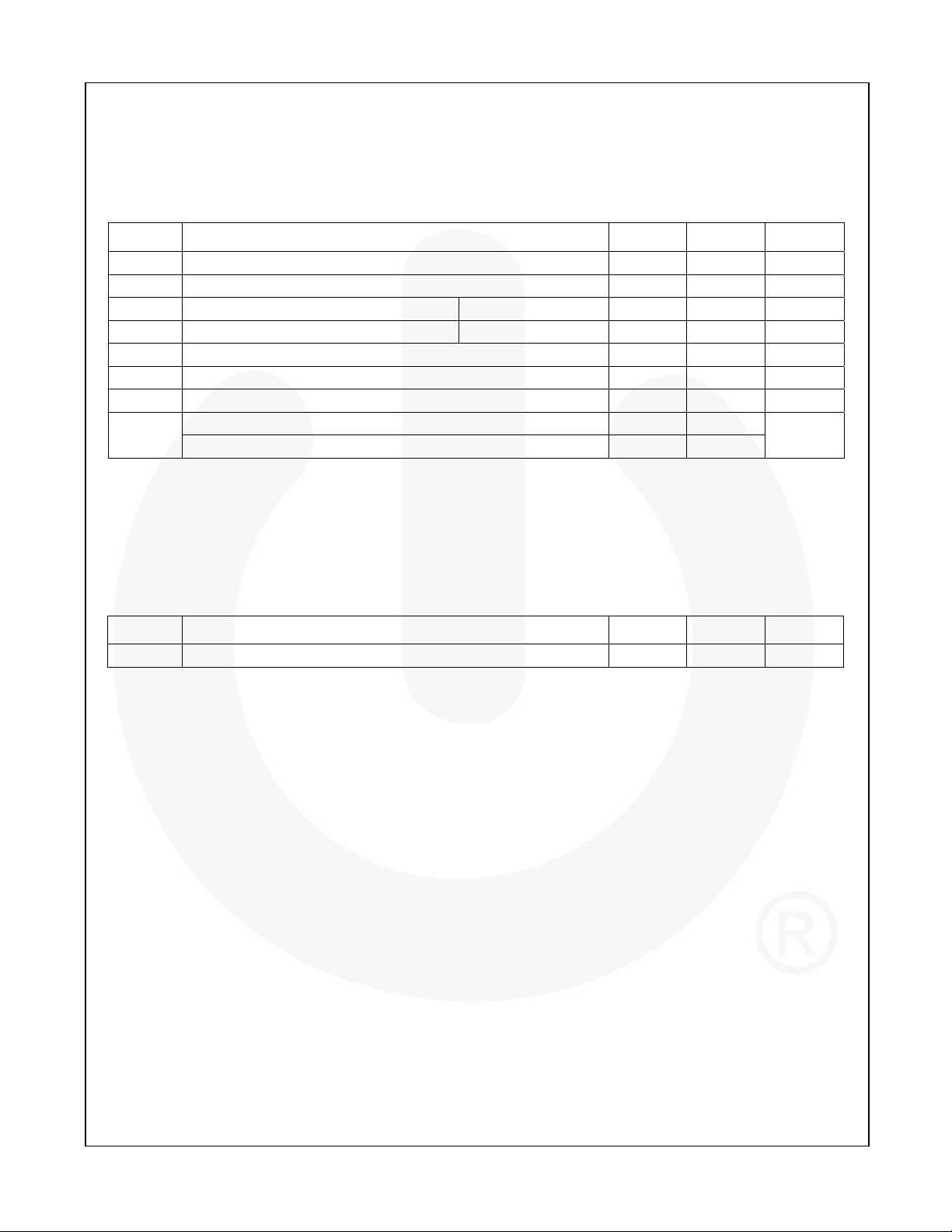
Absolute Maximum Ratings
Stresses exceeding the absolute maximum ratings may damage the device. The device may not function or be
operable above the recommended operating conditions and stressing the parts to these levels is not recommended.
In addition, extended exposure to stresses above the recommended operating conditions may affect device
reliability. The absolute maximum ratings are stress ratings only. All voltage values, except differential voltages, are
given with respect to GND pin.
Symbol Parameter Min. Max. Unit
VDD Supply Voltage 30 V
VL Input Voltage to FB, SENSE, VIN, RT, RI Pins -0.3 7.0 V
PD Power Dissipation at TA<50°C SOP 400 mW
JC Thermal Resistance (Junction-to-Case) SOP 54.4 °C/W
TJ Operating Junction Temperature -40 +150 °C
T
Storage Temperature Range -65 +150 °C
STG
TL Lead Temperature, Wave Soldering, 10 Seconds +260 °C
ESD
Human Body Model, JESD22-A114 5.0
Charge Device Model, JESD22-C101 1.5
kV
Recommended Operating Conditions
The Recommended Operating Conditions table defines the conditions for actual device operation. Recommended
operating conditions are specified to ensure optimal performance to the datasheet specifications. Fairchild does not
recommend exceeding them or designing to Absolute Maximum Ratings.
Symbol Parameter Min. Max. Unit
TA Operating Ambient Temperature -40 +105 °C
© 2008 Fairchild Semiconductor Corporation www.fairchildsemi.com
SG6846B • Rev. 1.3.4 5
Page 6
Electrical Characteristics
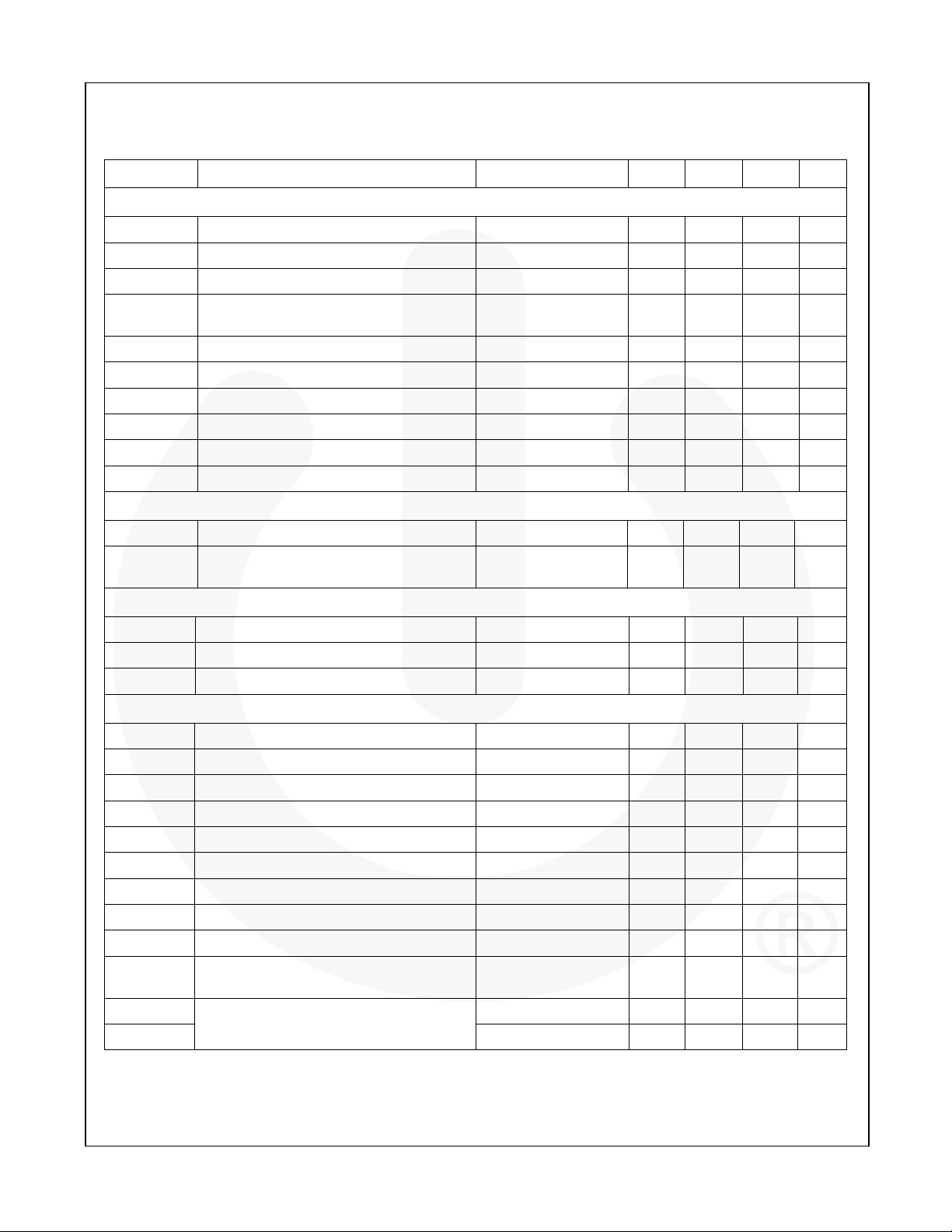
VDD = 15V and TA = 25°C unless otherwise noted.
Symbol Parameter Test Condition Min. Typ. Max. Unit
VDD Section
V
Continuously Operating Voltage 20 V
DD-OP
V
Turn-on Threshold Voltage 15.5 16.5 17.5 V
DD-ON
V
Turn-off Voltage 9.5 10.5 11.5 V
DD-OFF
V
DD-SCP
V
Threshold Voltage for Latch-off Release 3 4 5 V
DD-LH
I
Startup Current V
DD-ST
I
Operating Supply Current GATE Open 3.7 5.0 mA
DD-OP
V
VDD Over-Voltage Protection (Latch off) 23 24 25 V
DD-OVP
t
D-VDDOVP
VDD OVP Debounce Time RI = 26k 150 µs
I
VDD OVP Latch-off Holding Current VDD = 5V 30 50 70 µA
DD-OVP
VIN Section
Threshold Voltage on VDD for Short-Circuit
Protection
– 0.16V 8 30 µA
DD-ON
V
DD-OFF
+0.5V
V
DD-OFF
+1.0V
V
DD-OFF
+1.5V
SG6846B — Highly Integrated Green-Mode PWM Controller
V
V
PWM Turn-off Threshold Voltage 0.65 0.70 0.75 V
IN-OFF
V
PWM Turn-on Threshold Voltage
IN-ON
V
IN-OFF
+0.18
V
IN-OFF
+0.20
V
IN-OFF
+0.22
Feedback Input Section
AV Input-Voltage to Current-Sense Attenuation 1/3.5 1/4.0 1/4.5 V/V
ZFB Input Impedance 4.0 5.5 7.0 k
V
FB Pin Open Voltage 5.2 6.2 6.6 V
FBO
Current Sense Section
Z
Input Impedance 12 k
SENSE
tPD Delay to Output 100 250 ns
t
Leading-edge Blanking Time 270 360 ns
LEB
V
SLOPE
V
STH1V
V
STH3V
V
STH1V-2/3
V
STH3V-2/3
t
D-OCP
t
D-Short
t
SS-65KHz
t
SS-130KHz
Slope Compensation Duty = DCY
Threshold Voltage for Current Limit VIN = 1V 0.80 0.83 0.86 V
Threshold Voltage for Current Limit VIN = 3V 0.67 0.70 0.73 V
OCP Threshold Voltage for Current Limit VIN = 1V 0.58 0.61 0.64 V
OCP Threshold Voltage for Current Limit VIN = 3V 0.48 0.51 0.54 V
Delay Time for Over-Current Protection RI = 26k 175 200 225 ms
V
> V
Output Short Circuit Protection delay time
R
Period During Soft Start Time
CS
V
< V
DD
= 26k 4.5 5.0 5.5 ms
I
RI = 13k 2.25 2.50 2.75 ms
0.30 0.33 0.36 V
MAX
, RI = 26k,
STH
DD-SCP
6 7 8 ms
Continued on following page…
V
© 2008 Fairchild Semiconductor Corporation www.fairchildsemi.com
SG6846B • Rev. 1.3.4 6
Page 7
SG6846B — Highly Integrated Green-Mode PWM Controller
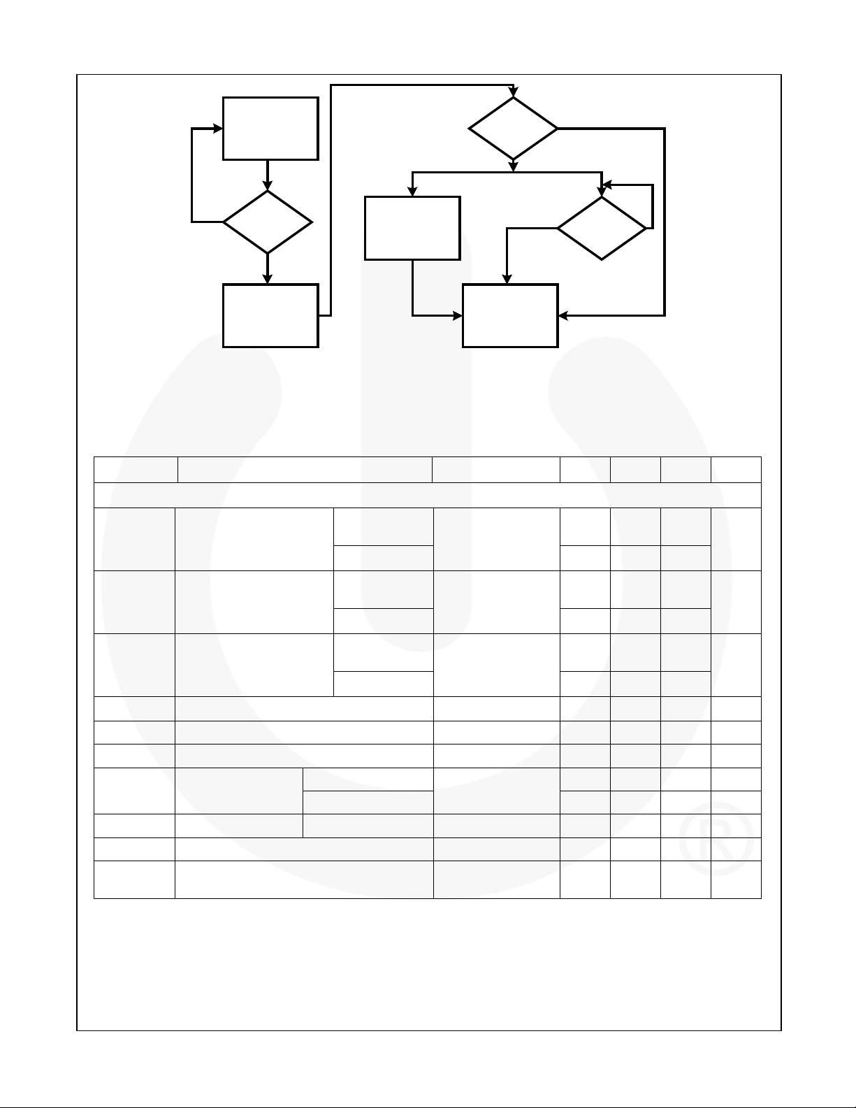
( 1 ) no rm a l
ope r a t i on
N
O
I P > 2 / 3 I
T i m i ng = 8 m s
( 2 )
( 3 )
PK
?
(5 )
Timing= 200 ms
OCP
(4 )
V
< 12 V?
DD
NO
SCP
(7 ) Gate-off
YES
V
YES
DD
SCP
NO
(6 )
<= 12 V ?
Figure 6. SG6846B OCP/SCP Logic Flow Diagram
Electrical Characteristics (Continued)
VDD = 15V and TA = 25°C unless otherwise noted.
Symbol Parameter Test Condition Min. Typ. Max. Unit
Oscillator Section
Center
f
Normal PWM Frequency
OSC
Frequency
RI = 26k, VFB>VN
Jitter Range
Center
f
OSC,MAX
Maximum PWM
Frequency
Frequency
R
= 13k, VFB>VN
I
Jitter Range
Center
f
Minimum PWM Frequency
OSC,MIN
Frequency
RI = 36k, VFB>VN
Jitter Range
t
hop-1
f
OSC-G
Jitter Period
RI = 26k, VFB ≥ VN
Green-Mode Minimum Frequency RI = 26k 18.0 22.5 25.0 kHz
62 65 68
±3.7 ±4.2 ±4.7
124 130 136
±7.4 ±8.4 ±9.4
44.8 47.0 49.2
±2.54 ±2.90 ±3.26
3.9 4.4 4.9 ms
SG Slope for Green-Mode Modulation RI = 26k 85 Hz/mV
V
V
FB-N
FB-G
FB Pin Frequency
Reduction Threshold
FB Voltage at f
OSC-G
Pin, FB voltage 1.9 2.1 2.3 V
RI = 26k, VFB = VN
Jitter Range
3.7 4.2 4.7 KHz
Pin, FB voltage RI = 26k, VFB = VG 1.4 1.6 1.8 V
fDV Frequency Variation vs. VDD Deviation VDD = 11.5V to 20V 5 %
fDT
Frequency Variation vs. Temperature
Deviation
TA = -30 to 85°C 1.5 5.0 %
Continued on following page…
kHz
kHz
kHz
© 2008 Fairchild Semiconductor Corporation www.fairchildsemi.com
SG6846B • Rev. 1.3.4 7
Page 8

SG6846B — Highly Integrated Green-Mode PWM Controller
Electrical Characteristics (Continued)
VDD = 15V and TA = 25°C unless otherwise noted.
Symbol Parameter Test Condition Min. Typ. Max. Unit
PWM Output Section
DCY
Maximum Duty Cycle 80 85 90 %
MAX
VOL Output Voltage Low VDD = 15V, IO = 50mA 1.5 V
VOH Output Voltage High VDD = 12V, IO = 50mA 8 V
tR Rising Time GATE = 1nF 350 ns
tF Falling Time GATE = 1nF 50 ns
V
Gate Output Clamping Voltage VDD = 20V 18 V
CLAMP
Over-Temperature Protection (OTP) Section
(1)
IRT Output Current of RT Pin RI = 26k 64 70 76 µA
V
RTTH
Threshold Voltage for OTP 1.00 1.05 1.10 V
SG6846BLSY or
t
DOTP-LATCH
R
RT-OFF
Over-Temperature Latch-off Debounce
Equivalent Impedance of RT for OTP
(1)
SG6846BCSY,
R
= 26k, VFB>VN
I
SG6846BLSZ or
SG6846BCSZ,
R
= 26k, VFB>VN
I
R
= 26k 14 15 16 k
I
100 ms
100 µs
RI Section
RI
NOR
RI
MAX
RI
MIN
Note:
1. The relationship between R
RI Operating Range 13 36 k
Maximum RI Value for Protection 10 M
Minimum RI Value for Protection 6 k
RT-OFF
and RI is: ))(K R / 26 A (70 / V I / VR
μ
Ω×==
IRTRTOFF-LATCH-OTPOFF-RT
(1)
© 2008 Fairchild Semiconductor Corporation www.fairchildsemi.com
SG6846B • Rev. 1.3.4 8
Page 9
Typical Performance Characteristics
SG6846B — Highly Integrated Green-Mode PWM Controller
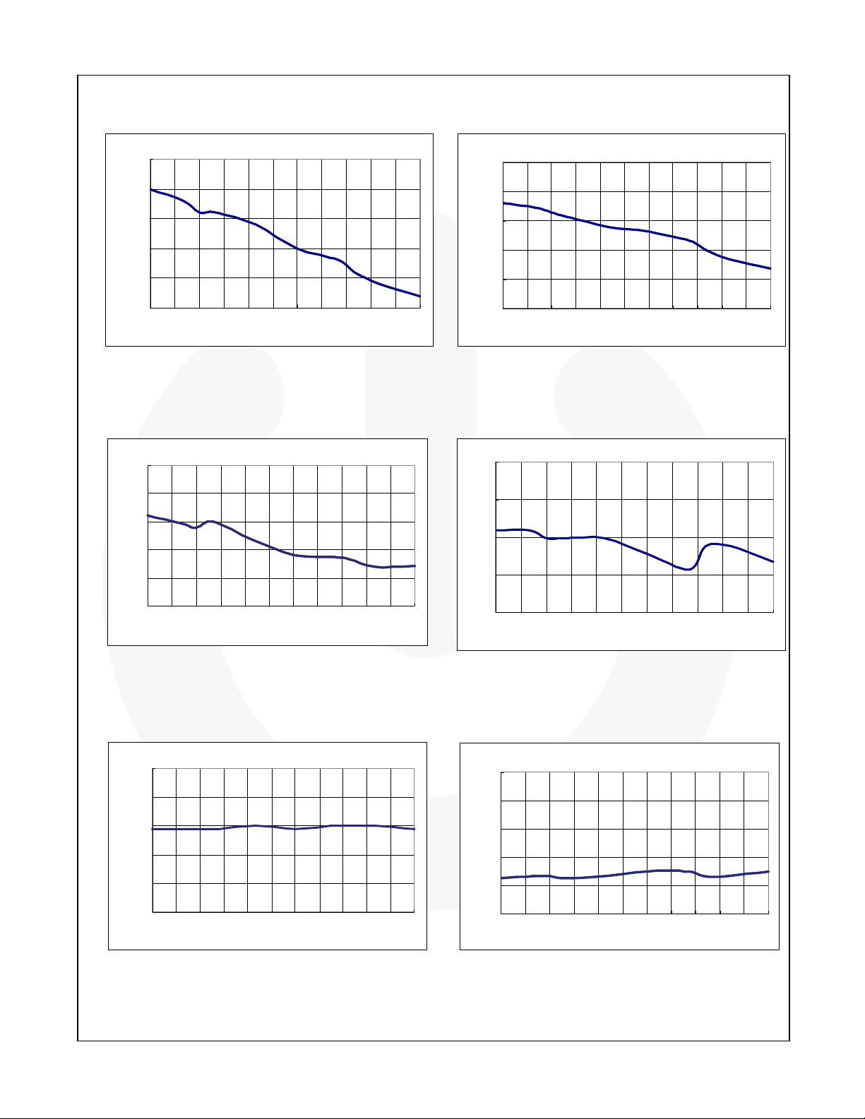
17.0
16.8
16.6
(V)
16.4
DD-ON
V
16.2
16.0
Turn-on Th r esho ld Voltage (V
-40 -25 -10 5 20 35 50 65 80 95 110 125
Temperature (℃)
Figure 7. Turn-on Threshold Voltage (V
vs. Temperature
) vs Temperature
DD-ON
DD-ON
)
Turn-off Voltage (V
11.5
11.0
10.5
(V)
10.0
DD-OFF
V
9.5
9.0
-40 -25 -10 5 20 35 50 65 80 95 1 10 125
Temperature (℃)
) vs Temperature
DD-OFF
Figure 8. Turn-off Threshold Voltage (V
vs. Temperature
DD-OFF
)
Operating Supply Current (IDD-op) vs Temperature
(µA)
DD- ST
I
26.0
22.0
18.0
14.0
10.0
Startup Current (I
) vs Temperature
DD-ST
6.0
5.5
5.0
IDD-o p ( mA)
4.5
6.0
-40 -25 -10 5 20 35 50 65 80 95 110 125
Temperature (℃)
Figure 9. Startup Current (I
) vs. Temperature Figure 10. Operating Supply Current (I
DD-ST
4.0
-40 -25 -10 5 20 35 50 65 8 0 95 110 125
Temperature (℃)
DD-op
) vs.
Temperature
OCP Thre s hold Voltage for C urrent Limit (V
0.66
0.64
0.62
(V)
0.60
STH1V-2/3
V
0.58
0.56
-40 -25 -10 5 20 35 50 65 80 95 110 1 25
Temperature
Temperature (℃)
Figure 11. OCP Threshold Voltage for Current Limit
(V
) vs. Temperature
STH1V-2/3
STH1V-2/3
)vs
OC P ThresholdVoltagefor Cu rrent Lim it(V
0.60
0.58
0.56
(V)
0.54
STH3V-2/3
V
0.52
0.50
-40 -25 -10 5 20 3 5 50 65 80 95 110 125
Temperature
STH3V-2/3
Temperature (℃)
Figure 12. OCP Threshold Voltage for Current Limit
(V
) vs. Temperature
STH3V-2/3
)vs
© 2008 Fairchild Semiconductor Corporation www.fairchildsemi.com
SG6846B • Rev. 1.3.4 9
Page 10
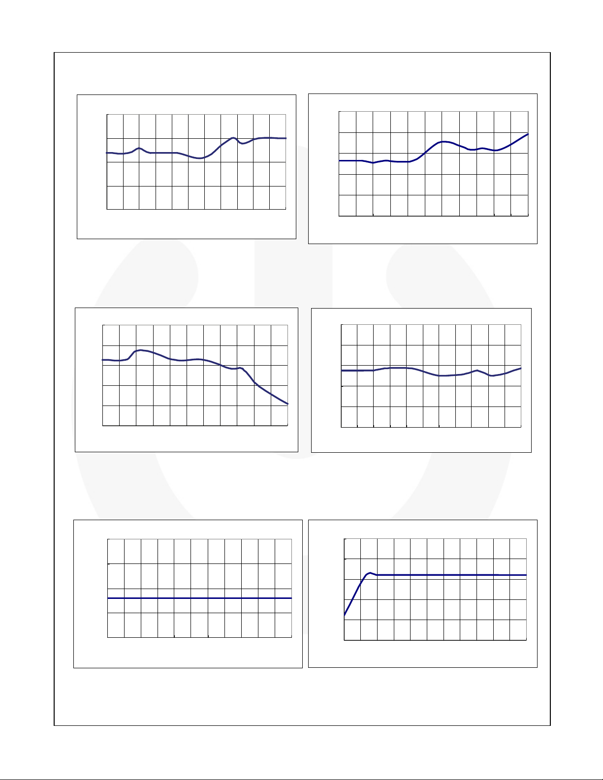
Typical Performance Characteristics (Continued)
SG6846B — Highly Integrated Green-Mode PWM Controller
NormalPWM Frequency (f
64.0
63.5
63.0
(kHz)
OSC
f
62.5
62.0
-40 -25 -10 5 20 35 50 65 80 95 110 12 5
Temperature (℃)
)vs Temper ature
OSC
Figure 13. Normal PWM Frequency (f
vs. Temperature
OSC
87.2
87.0
86.8
86.6
DCYmax (%)
86.4
86.2
)
Maximum Duty C ycle (DCYmax) vs Temp er ature
-40 -25 -10 5 20 35 50 65 80 95 110 125
Temperatu r e (℃)
Figure 14. Maximum Duty Cycle (D
CYmax
)
vs. Temperature
(µA)
RT
I
70.8
70.6
70.4
70.2
70.0
Ou tp ut Current o fRTPin (IRT)vs Tempe rature
(V)
RTTH
V
1.10
1.08
1.06
1.04
1.02
Trigger Voltage of OTP (V
)vs Temper atur e
RTTH
69.8
-40 -25 -10 5 20 35 50 65 80 95 110 125
Temperature (℃)
Figure 15. Output Current of RT pin (IRT)
vs. Temperature
1.00
-40 -25 -10 5 20 35 50 65 80 95 110 125
Temperature (℃)
Figure 16. Trigger Voltage of OTP(V
RTTH
vs. Temperature
)
PWM Turn-on Threshold Voltage (V
0.925
0.920
(V)
0.915
IN-ON
V
0.910
0.905
-40 -25 -10 5 20 35 50 65 80 95 110 125
Temperatur e (℃)
) vs Temperature
IN-ON
Figure 17. PWM Turn-on Threshold Voltage (V
vs. Temperature
IN-ON
PWM Turn-off Threshold Voltage (V
0.715
0.710
0.705
(V)
0.700
IN-OFF
V
0.695
0.690
-40 -25 -10 5 20 35 50 65 80 95 110 125
Temperature (℃)
)
Figure 18. PWM Turn-off Threshold Voltage (V
vs. Temperature
) vs Temperature
IN-O FF
IN-OFF
)
© 2008 Fairchild Semiconductor Corporation www.fairchildsemi.com
SG6846B • Rev. 1.3.4 10
Page 11
Operation Description
SG6846B — Highly Integrated Green-Mode PWM Controller
Startup Operation
The turn-on/turn-off thresholds are fixed internally at
16.5V and 10.5V. To enable the SG6846B during
startup, the hold-up capacitor must first be charged to
16.5V through the startup resistor.
If an open-circuit or short-circuit to ground occurs at the
RI pin, the internal protection circuit immediately shuts
down the controller.
The hold-up capacitor continues to supply V
before
DD
energy can be delivered from the auxiliary winding of
the main transformer. The V
must not drop below
DD
10.5V during this startup process. This UVLO hysteresis
window ensures that the hold-up capacitor can
adequately supply V
during startup.
DD
The typical startup current is only 8µA, which allows a
high-resistance, low-wattage startup resistor to be used.
For constant output power limit over a universal inputvoltage range, the peak-current threshold is adjusted by
the voltage of the VIN pin. Since the VIN pin is
connected to the rectified AC input line voltage through
the resistive divider, a higher line voltage generates a
higher V
the V
voltage. The threshold voltage decreases as
IN
increases, making the maximum output power at
IN
high line input voltage equal to that at low line input.
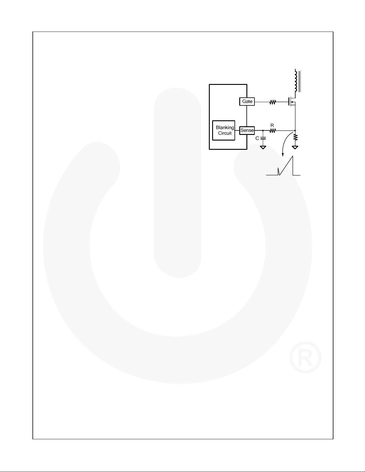
The value of R-C network should not be so large it
affects the power limit (shown in Figure 19). R and C
should put on less than 300 and 1000pF, respectively,
to minimize power loss. A 1.5M/0.25W startup resistor
and a 10µF/25V V
hold-up capacitor are sufficient for
DD
a universal input range.
The required operating current has been reduced to
3.7mA, which enables higher efficiency and reduces the
V
hold-up capacitance requirement.
DD
Green-Mode Operation
The proprietary green-mode function provides off-time
modulation to continuously decrease the switching
frequency under light-load conditions. Maximum on-time
is limited to provide protection against abnormal
conditions. To further reduce power consumption under
zero-load condition, the PWM oscillator is completely
turned off and the power supply enters burst-mode.
Green mode dramatically reduces power consumption
under light-load and zero-load conditions. Power
supplies using SG6846B can meet restrictive
international regulations regarding standby power
consumption.
Oscillator Operation
A resistor connected from the RI pin to GND generates
a internal reference current source used to determine
the PWM frequency. Increasing the resistance
decreases the amplitude of the current source and
reduces the PWM frequency. Using a 26kΩ resistor
results in a corresponding 65kHz switching frequency.
The relationship between R
frequency is:
and the switching
I
1690
f
(kHz)
PWM
=
)(kR
Ω
I
(2)
If an open-circuit or short-circuit to ground occurs at the
RI pin, the internal protection circuit immediately shuts
down the controller.
Two-level Over-current Protection (OCP)
The cycle-by-cycle current limiting shuts down the PWM
immediately when the switching current is over the
peak-current threshold. Additionally, when the switching
current is higher than over-current threshold, the internal
counter counts down. When the total accumulated
counting time is more than ~200ms (R
= 26k), the
I
controller is latched off and the internal counter counts
up. When the switching current is lower than overcurrent threshold, the internal counter counts down.
When the total accumulated counting time is more than
~200ms (R
= 26k), the controller is latched off.
I
This two-level OCP protection and up/down counter are
especially designed for SMPS with surge current output,
such as those for printers, scanners, and motor drivers.
Constant Output Power Limit
For constant output power limit over universal inputvoltage range, the peak-current threshold is adjusted by
the voltage of the VIN pin. Since the VIN pin is
connected to the rectified AC input line voltage through
the resistive divider, a higher line voltage generates a
higher V
V
IN
voltage. The threshold voltage decreases as
IN
increases, making the maximum output power at
high-line input voltage equal to that at low-line input.
Brownout Protection
Since the VIN pin is connected through a resistive
divider to the rectified AC input line voltage, it can also
be used for brownout protection. If the V
less than 0.7V, the PWM output is shut off. If the V
voltage is
IN
is
IN
over 0.9V, the PWM output is turned on again. The
hysteresis window for on/off is ~0.2V.
VDD Over-voltage Protection (OVP)
VDD over-voltage protection is built in to prevent
damage. If V
is over 24V, SG6846B is latched off.
DD
Over-Temperature Protection (OTP)
An external NTC thermistor can be connected from the
RT pin to GND. The impedance of the NTC decreases
at high temperatures. When the voltage of the RT pin
drops below 1.05V, the SG6846B is turned off. For
protection-mode options, see Ordering Information.
© 2008 Fairchild Semiconductor Corporation www.fairchildsemi.com
SG6846B • Rev. 1.3.4 11
Page 12
Operation Description (Continued)
Noise Immunity
Noise from the current sense or the control signal may
cause significant pulse-width jitter, particularly in
continuous-conduction mode. Slope compensation
helps alleviate this problem. Good placement and
layout practices should be followed. Avoid long PCB
traces and component leads. Compensation and filter
components should be located near the SG6846B.
SG6846B — Highly Integrated Green-Mode PWM Controller
Figure 19. Current Sense R-C Filter
© 2008 Fairchild Semiconductor Corporation www.fairchildsemi.com
SG6846B • Rev. 1.3.4 12
Page 13
P1
Reference Circuit
RT1
F1
P2
P7
t
VZ1
1 2
LF1
CY2
3 4
CY1
CX1
34
LF2
SG6846B — Highly Integrated Green-Mode PWM Controller
2
12
CX2
R2
R1
R3
R4
BD1
4
1
21
+
R8
3
R9
21
+
C3
D1
C2
R12
21
1 2
21
+
C5
C4
D2
21
D3
L4
21
R11
TX1
5
6
7 9
1
3
13
10
11
R16
D4
2
R17
2
C16
C17
21
21
P32V
P32V
+
P16V
P16V
+
L1
21
C12
+
L2
21
C14
+
32V
32V
21
C13
+
16V
16V
21
C15
+
1
3
C11
1
3
D5
U1
1
FB
2
21
C1
3
+
R5
4
R7
8
GND
GATE
7
FB
VDD
6
VIN
SENSE
R10
5
RI
RT
R13
C6
NTC1
23
Q1
1
L3
R6
1 2
R14
P16V
P16V
R15
FB
FB
C7
12
43
C9
U2
A K
P16V P32V
R19
R21
P32VP16V
R20
R18
R
U3
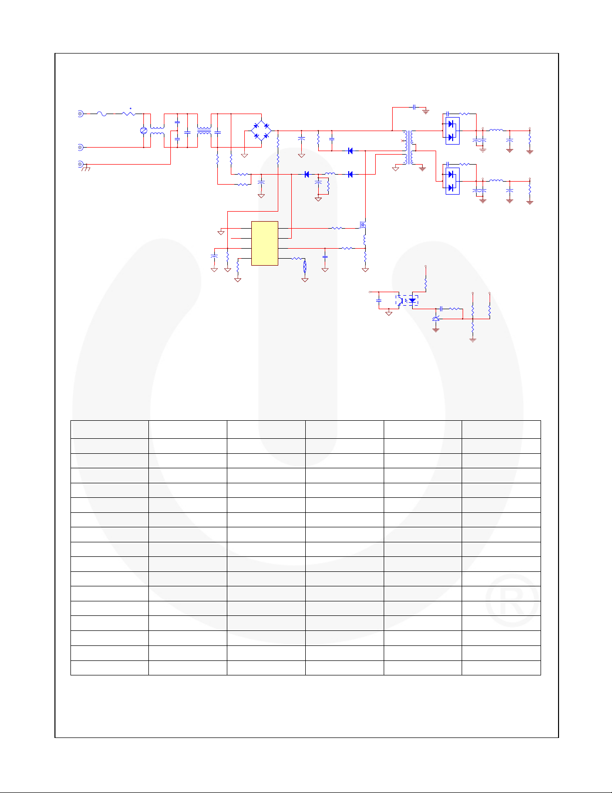
Figure 20. Application Circuit for 32V / 16V Output
BOM
Part No. Value Part No. Value Part No. Value
R1, R2, R3, R4 470K +/-5% C4 103P 630V D3 FR103 1.0A 200V
R8, R9 S1M +/-1% C10,C11 102P 1KV BD1 DBL406G
R5 16K2 +/-1% C6,C7 102P 50V D4 BYT28-300
R15 1K5 +/-5% C9 222P 50V D5 BYV32-150
R13 10 +/-5% C14,C17 470µ 25V F1 250V4A QUICK
R18 4K7 +/-5% C15 220µ 25V L1,L2 1.8µH
R21 15K +/-1% C13,C16 220µ 50V L4 10µH
R7 27K +/-5% C2 150µ 400V U3 TL431 +/-1%
R6 330 +/-1% C1 4.7µ 50V U1 SG6846
R19 102K +/-1% C3 10µ 50V U2 PC817
R14 022 +/-5% CX1 X1 0.47µ 275V Q1 7NB60
R16, R17 1W 20 +/-5% C8 Y2 222P 250V TX1 EI-33
R11 20K +/-5% C5 100µ 50V RT1 SCK053
R12 100K +/-5% CX2 X2 0.1µF 275V VZ1 14 470V
R20 887K +/-1% D1 1N4148
R22 10K +/-1% D2 BYV95C
© 2008 Fairchild Semiconductor Corporation www.fairchildsemi.com
SG6846B • Rev. 1.3.4 13
Page 14
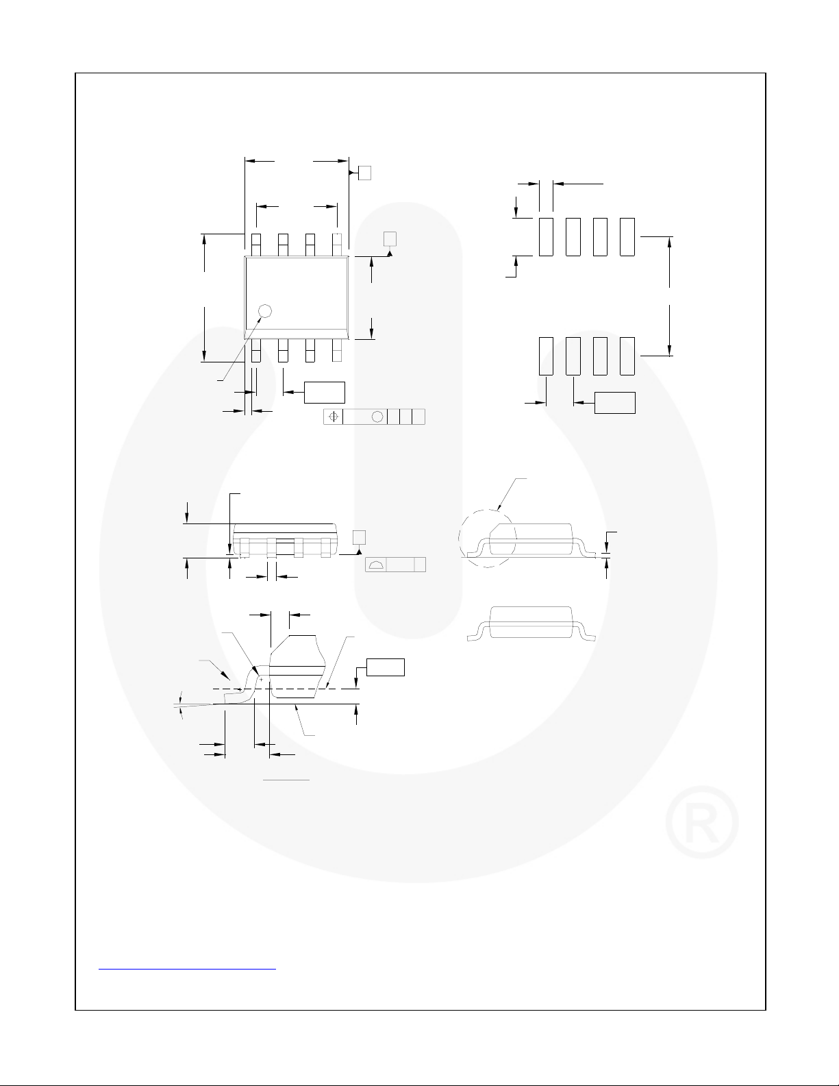
Physical Dimensions
8
5.00
4.80
3.81
SG6846B — Highly Integrated Green-Mode PWM Controller
A
0.65
5
B
6.20
5.80
PIN ONE
INDICATOR
(0.33)
1.75 MAX
R0.10
R0.10
8°
0°
0.90
0.406
1
0.25
0.10
DETAIL A
SCALE: 2:1
4
1.27
0.51
0.33
0.50
0.25
SEATING PLANE
(1.04)
4.00
3.80
CMBA0.25
C
0.10 C
x 45°
GAGE PLANE
0.36
1.75
5.60
1.27
LAND PATTERN RECOMMENDATION
SEE DETAIL A
0.25
0.19
OPTION A - BEVEL EDGE
OPTION B - NO BEVEL EDGE
NOTES: UNLESS OTHERWISE SPECIFIED
A) THIS PACKAGE CONFORMS TO JEDEC
MS-012, VARIATION AA, ISSUE C,
B) ALL DIMENSIONS ARE IN MILLIMETERS.
C) DIMENSIONS DO NOT INCLUDE MOLD
FLASH OR BURRS.
D) LANDPATTERN STANDARD: SOIC127P600X175-8M.
E) DRAWING FILENAME: M08AREV13
Figure 21. 8-Pin Small Outline Package (SOP)
Package drawings are provided as a service to cust omers considering Fairchild components. Drawings may change in any manner
without notice. Pl ease note the revision and/or date on t he drawing and contact a Fairchild S emic onductor representative to ver ify
or obtain the most recent revision. Package specifications do not expand the terms of Fairchild’s worldwide terms and conditions, specifically
the warranty therein, which covers Fairchild products.
Always visit Fairchild Semiconductor’s online packaging area for the most recent package drawings:
http://www.fairchildsem i.com/p ackagi ng/
© 2008 Fairchild Semiconductor Corporation www.fairchildsemi.com
SG6846B • Rev. 1.3.4 14
.
Page 15
SG6846B — Highly Integrated Green-Mode PWM Controller
© 2008 Fairchild Semiconductor Corporation www.fairchildsemi.com
SG6846B • Rev. 1.3.4 15
 Loading...