

Page 1
Product Specification
High-integrated Green-mode PWM Controller SG6841
FEATURES
Green-mode PWM to support “Blue Angel” Norm
Low start up current 30uA
Low operation current 3mA
Leading-edge blanking
Built-in synchronized slope compensation
Constant output power limit for universal AC input
Current mode operation
Cycle-by-cycle current limiting
Under voltage lockout (UVLO)
Programmable PWM frequency
GATE output maximum voltage clamped at 18V
Totem pole output includes soft driving for better
EMI
Build-in limited-power-control to meet safety
requirement
Programmable over-temperature protection
Few external components & low cost solution
APPLICATIONS
General-purpose switching mode power supplies
and flyback power converters, and
Power Adapter
Open-frame SMPS
Battery Charger Adapter
DESCRIPTION
This highly integrated PWM controllers, SG6841 series,
provides several features to enhance the performance of
low power flyback converters. To minimize standby
power consumption, the proprietary green-mode
function provides off-time modulation to linearly
decrease the switching frequency under light-load
conditions. This green-mode function assists the power
supply to easily meet the power conservation
requirement. Due to BiCMOS process, the start-up
current and operation current is reduced to 30uA and
3mA, respectively, to improve power conversion
efficiency. Large start-up resistance can be used for
further power saving. Built-in synchronized slope
compensation ensures the stability of peak current mode
control. A proprietary internal compensation ensures
constant output power limit for universal AC input
voltage from 90VAC to 264VAC.
SG6841 provides many protection functions.
Pulse by pulse current limit ensures a constant output
current under short circuit. If a short circuit failure or
over load happens, the SG6841 will shut off after a
continuous high voltage detection on FB pin. The gate
output is clamped at 18V to protect the power MOS
from over voltage damage. An external NTC
thermistor can be applied to sense the ambient
temperature for over-temperature protection. The
SG6841 series are available in 8-pin DIP and SO
packages.
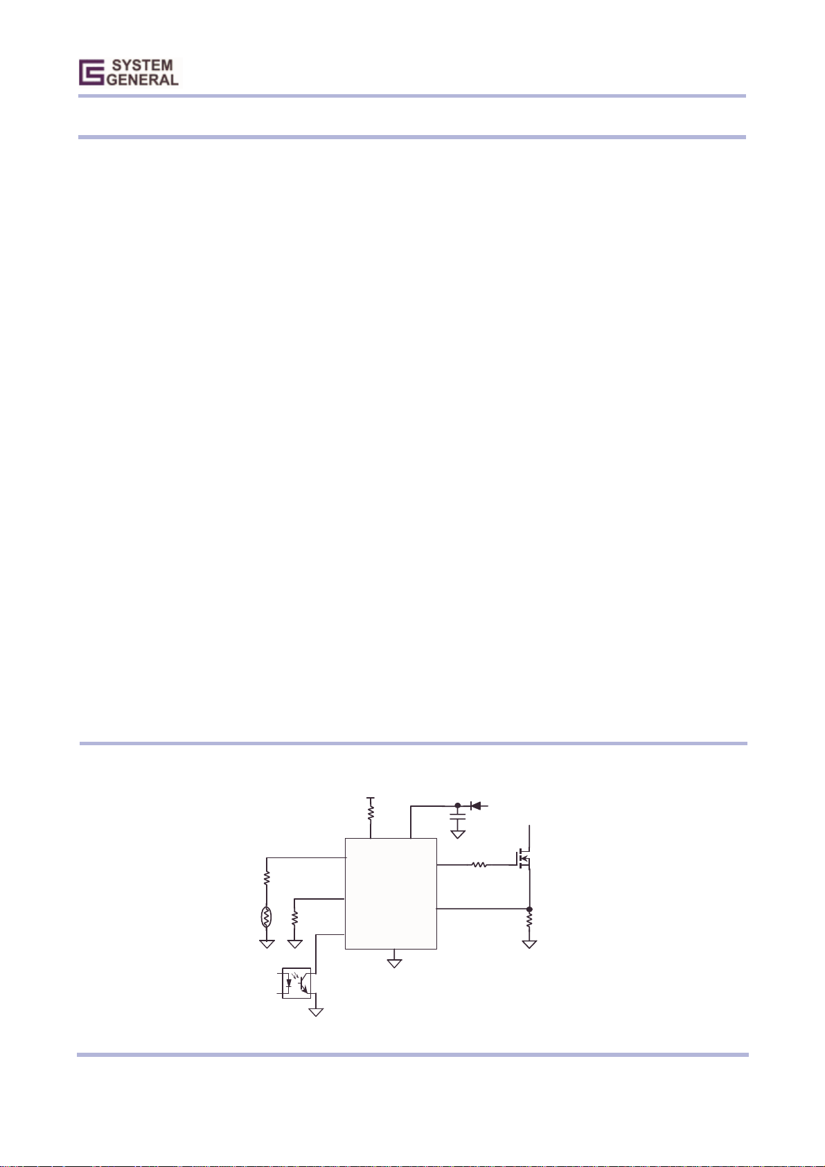
TYPICAL APPLICAT ION
From bridge re ctifie r
127~ 373VDC
RT
RA
RIN
VIN
RT
SG6842
RI
RI
FB
GND
VDD
GATE
SENSE
C
IN
©System General Corp. - 1 - www.sg.com.tw
Version 1.7 (IRO33.0001.B1) JUL.25,2003
D1
Rg
From auxiliary
winding
Q1
R
S
Page 2
Product Specification
High-integrated Green-mode PWM Controller SG6841
MARKING DIAGRAMS
8
T: D = DIP, S = SOP
XXXXXXX: Wafer Lot
SG6841T
XXXXXXXYYWWV
YY: Year; WW: Week
V: Assembly Location
1
ORDERING INFORMATION
Part Number Package
SG6841S 8-Pin SOP
SG6841D 8-Pin DI P
PIN DESCRIPT IONS
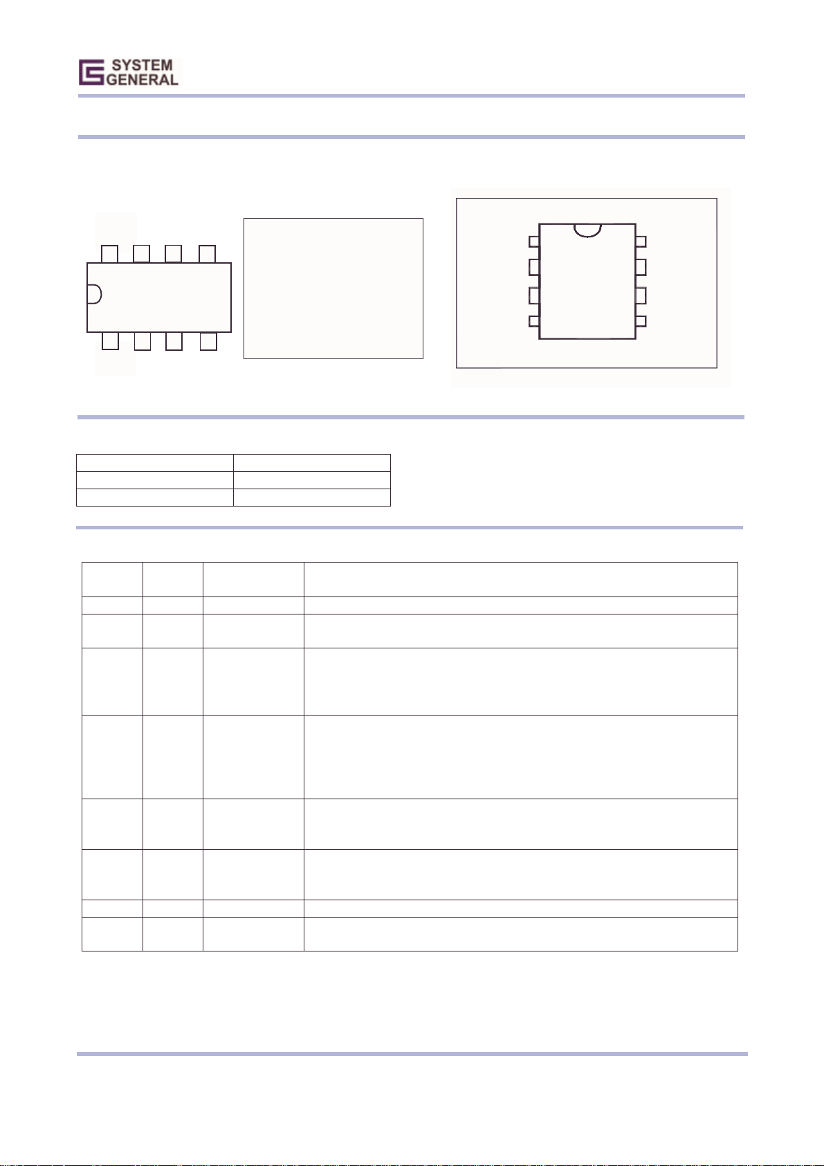
PIN CONFIGURATION
GND
FB
VIN
Ri
1
2
3
4
Gate
8
VDD
7
Sense
6
5
RT
Pin No. Symbol Function Description
1 GND Ground Ground.
2 FB Feedback
3 VIN Start-Up Input
4 Ri Referenc e Setting
5 RT
6 SENSE Current S ense
7 VDD Power supply
8 GATE Driver Output
Temperature
Protec tion
The signal from external compensation circuit is feed into this pin. The PW M duty cycle is
determined by this FB pin and current sens e signal from Pin 6.
This pin is pulled high to the rectified line input through a resistor for start-up. Since the
start-up current requir ement f or SG6841 is very small, a large start-up resistance can be
used to minimize power loss. Under normal operation, this pin is also used to detect lin e
voltage to compensate for c onstant output power limit f or universal AC input.
A resistor from R I pin to ground will generate a const ant current source forSG6841. This
current is used to charge an internal capacitor and hence the switching fr equency are
determined. Increasing the resistance will decrease the current sourc e and reduce the
switching frequency. A 26kΩ resistor R
65kHz switching frequency.
For over-temperature protection. An external NTC thermistor is connected from this pin
to ground. The impedance of the NTC will decrease under high temperature. Once the
voltage on RT pin drops below a fixed limit, the PWM output will be disabled.
Current s ense. The s ensed voltage is used for current mode c ontrol and puls e-by-pulse
current limiting. If a short circuit failure happens on current sense resistor, the SG6841
will shut off after a continuous low voltage detection on SENSE pin.
Power Supply.
The totem-pole output driver for the power MOSFET. A soft driving waveform is
implemented to improve EMI.
creates a 50uA constant current Ii and generates
i
©System General Corp. - 2 - www.sg.com.tw
Version 1.7 (IRO33.0001.B1) JUL.25,2003
Page 3
Product Specification
High-integrated Green-mode PWM Controller SG6841
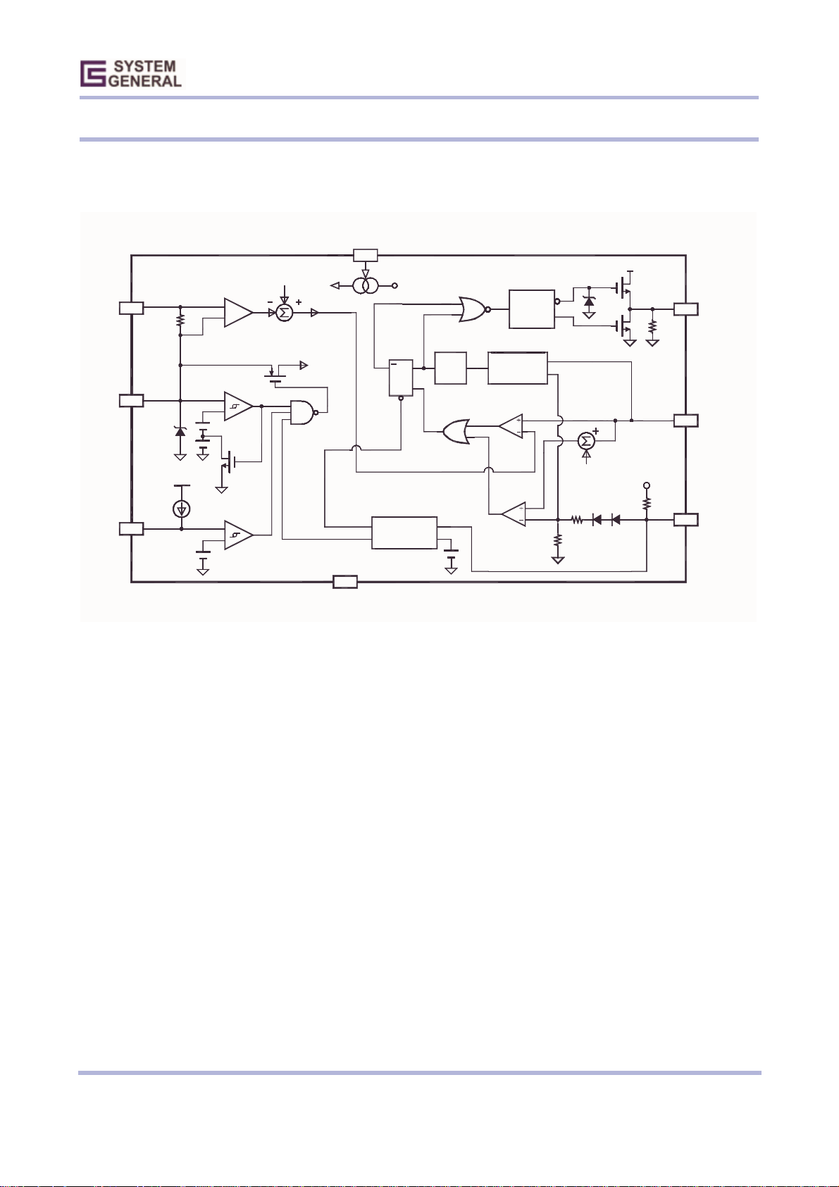
BLOCK DIAGRAM
1
GND
RI
4
QS
Limited Power
Controller
VDD
ON/OFF
Driver
OSC
R
4.2V
Green Mode
Controll er
Comp
Comp
Slope
Compensation
2R
R
8
GATE
6
SENSE
6V
2
FB
VIN
VDD
RT
0.85V
IRT
+
_
+
_
16V/10V
+
_
0.65V
UVLO
Internal
BIAS
3
7
5
©System General Corp. - 3 - www.sg.com.tw
Version 1.7 (IRO33.0001.B1) JUL.25,2003
Page 4
Product Specification
High-integrated Green-mode PWM Controller SG6841
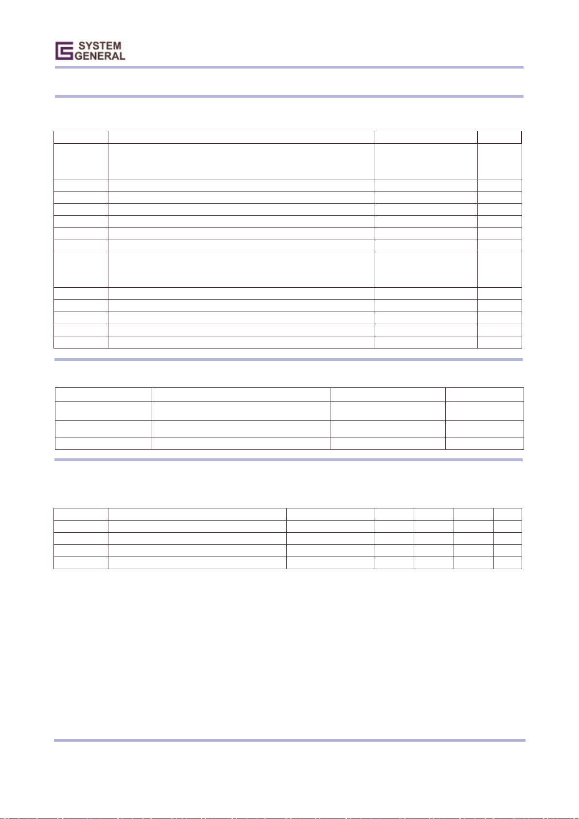
ABSOLUTE MAXIMUM RATINGS
Symbol Parameter Value Unit
VDD
I
Gate Out put Current 500 mA
OUT
VFB Input Voltage to FB Pin -0.3 to 7V V
V
Input Voltage to SENSE Pin -0.3 to 7V V
Sense
V
RT
VRI Input Voltage to Ri Pin -0.3 to 7V V
PD Power Dissipation 1 W
RΘ j-a
TJ Operating Junction T emperature 150 ℃
TA Operating Ambient T emperature -30 to 85 ℃
Tstg Storage Temperature Range -55 to +150 ℃
ESD Capability, HBM model 3.0 kV
ESD Capability, Machine model 250 V
DC Supply Voltage
Zener clamp
Zener current
Input Voltage to RT Pin -0.3 to 7V V
Thermal Resistance Junction-air
DIP
SOP
30
32
10
82.5
141
V
V
mA
℃/W
RECOMMENDED OPERATING CONDITIONS
Symbol Parameter Value Unit
VDD DC Supply Voltage <20 V
TA Operating Ambient Temperature -20 to +85
RI Current s ource Setting 26 kohms
℃
ELE CTRICAL CHARACTERISTICS
Feedback Input Section
Symbol Parameter Test Condition Min. Typ. Max. Unit
AV Input-voltage to current-sense attenuation 1/3.25 1/3 1/2.75 V/V
ZFB Input impedance 2 4.5 8 kΩ
IFB Bias current 2 mA
VOZ Input voltage for zer o duty cycle 1.2 V
©System General Corp. - 4 - www.sg.com.tw
Version 1.7 (IRO33.0001.B1) JUL.25,2003
Page 5
Product Specification
High-integrated Green-mode PWM Controller SG6841
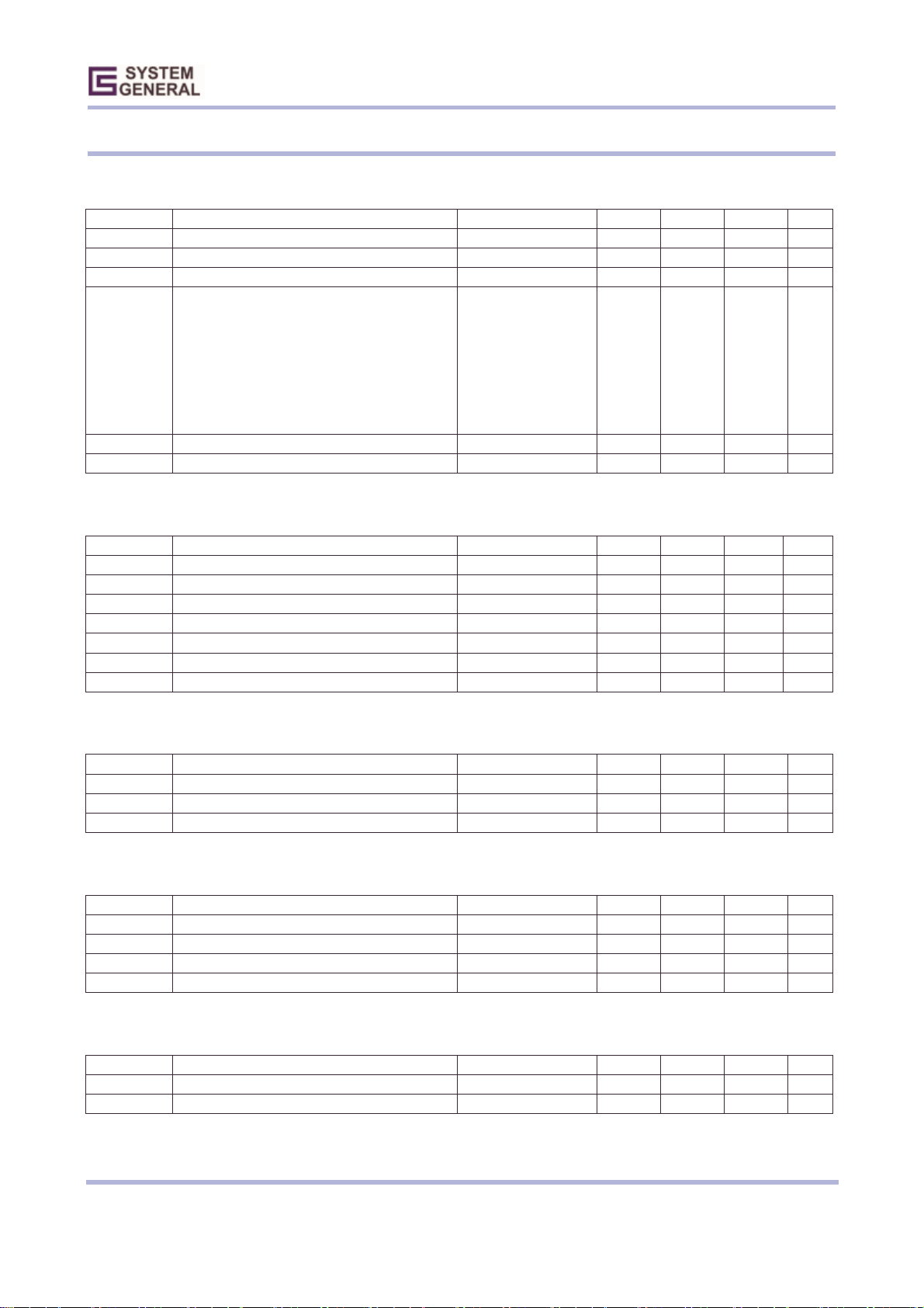
Current Sense Section
Symbol Parameter Test Condition Min. Typ. Max. Unit
ZCS Input impedance 8 12 16 KΩ
TPD Delay to Output 150 200 ns ec
VTH Threshold voltage for current limit I
= 0 uA 0.8 0.85 0.9 V
VIN
∆VTH @ I
V
Threshold voltage for I
SENSE0
Tdelay-lps The delay time of limited-power-control RI=26KOhms 31 msec
The change of threshold voltage versus the input
VIN
current of th e Vin
= 80uA I
VIN
I
= 220 uA -0.09 -0.15 -0.21 V
VIN
= 80 uA 0.73 0.81 0.89 V
VIN
Oscillator Section
Symbol Parameter Test Condition Min. Typ. Max. Unit
F
Frequency in nominal mode RI=26KOhms 60 65 70 KHz
OSC
Fosc-green Frequenc y in green mode RI=26KOhms 10 16 KHz
VG End of green mode volt age at FB pin 1.9 V
VN Beginning of frequency reducing at FB pin 2.6 V
SG Slope for green mode modulation RI=26KOhms 50 80 120 Hz/mV
FDV Frequenc y variation versus VDD deviation VDD=10 to 20V 5 %
FDT Frequency variation versus Temp. deviation TA=-30 to 85 ℃ 5 %
PWM Section
Symbol Parameter Test Condition Min. Typ. Max. Unit
DC
Maximum Duty Cycle 75 80 90 %
(MAX)
DC
Minimum Duty Cycle - - 0 %
(MIN)
Bnk Leading edge blanking time 200 270 350 nsec
Output Section
Symbol Parameter Test Condition Min. Typ. Max. Unit
VOL Output Voltage Low VDD = 12V, Io = 150mA 1.5 V
VOH Output Voltage High VDD = 12V, Io = 50mA 8V V
tr Rising Time VDD =13V, CL=1nF 150 250 350 nsec
tf Falling Time VDD =13V, CL=1nF 30 50 90 nsec
Under-voltage Lockout Section
Symbol Parameter Test Condition Min. Typ. Max. Unit
V
Start Threshold Voltage 15 16 17 V
TH(ON)
V
Min. Operating Voltage 9 10 11 V
DD(min)
©System General Corp. - 5 - www.sg.com.tw
Version 1.7 (IRO33.0001.B1) JUL.25,2003
Page 6
Product Specification
High-integrated Green-mode PWM Controller SG6841
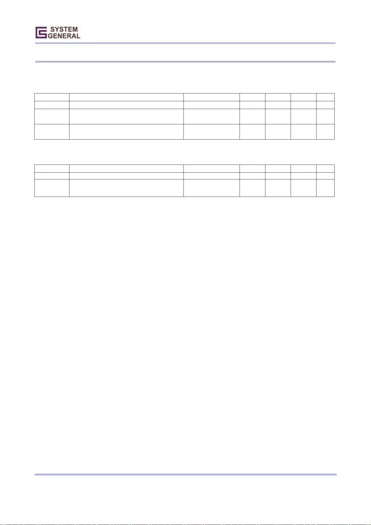
Over-Temperature Protection Section
Symbol Parameter Test Condition Min. Typ. Max. Unit
IRT Output current of pin RT RI=26KOhms 92 100 108 uA
V
OTP,STOP
V
OTP,START
Threshold voltage for over-temperature protection.
Turn-off point. Duty cycle is reduced to 0%.
Threshold voltage for over-temperature protection.
Starting point. Duty cycle starts to decrease.
0.585 0.62 0.655 V
0.65 V
Total Standby Current Section
Symbol Parameter Test Condition Min. Typ. Max. Unit
I
DD ST
I
DD OP
Start-up Current VDD=14.5V 30 40 uA
Operating Supply Curr ent FB=SENSE=0V
GATE=1000pF
VDD=15.5V
- 3 5 mA
©System General Corp. - 6 - www.sg.com.tw
Version 1.7 (IRO33.0001.B1) JUL.25,2003
Page 7
Product Specification
High-integrated Green-mode PWM Controller SG6841
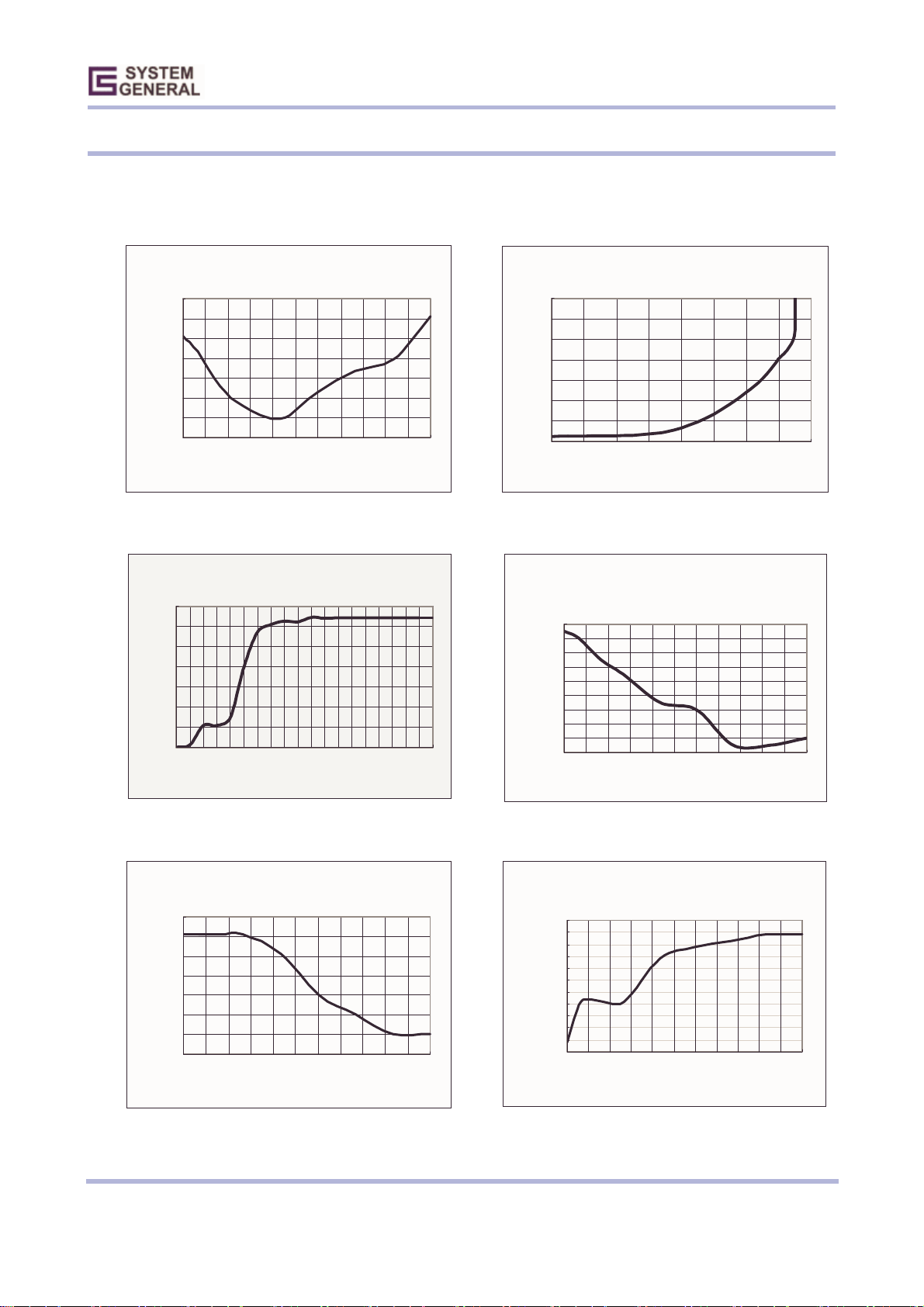
TYPICAL CHARACTERISTICS
S ta rt-up Current (I
25.5
25.0
24.5
24.0
23.5
23.0
22.5
Start-up Current (uA)
22.0
-40 -25 -10 5 20 35 50 65 80 95 110 125
TEMPERATURE (
) vs Temperature
DD ST
℃℃℃℃
)
Frequency vs. FB Voltage
70
60
50
40
30
20
Frequency (KHz)
10
0
1.1 1.4 1.7 2 2.3 2.6 2.9
FB VOLTAGE (V)
Start-up Current (I
35
30
25
20
15
10
5
Start-up Current (uA)
0
0 2 4 6 8 10 12 14 16
) vs VDD Voltage
DD ST
VDD VOLTAGE (V)
Frequency in green mode (Fosc-green) vs
Temperature
10.52
10.50
10.48
10.46
10.44
10.42
10.40
10.38
Fosc-green (KHz)
10.36
10.34
-40 -25 - 10 5 20 35 50 65 80 95 110 125
TEMPERATURE (℃℃℃℃)
PWM O sci l lat or Frequency (Fosc) vs
Tempe r ature
64.4
64.3
64.2
64.1
64.0
Fosc (KHz)
63.9
63.8
63.7
-40 -25 -10 5 20 35 50 65 80 95 110 125
TEMPERATURE (
)
℃℃℃℃
Max. Duty Cycle (%)
Maximum Duty Cycle DC(
MAX.
Tempe r ature
84.75
84.70
84.65
84.60
84.55
84.50
84.45
84.40
84.35
84.30
84.25
84.20
-40 -25 -10 5 20 35 50 65 80 95 110 125
TEMPERATURE (
)
℃℃℃℃
)vs
©System General Corp. - 7 - www.sg.com.tw
Version 1.7 (IRO33.0001.B1) JUL.25,2003
Page 8
Product Specification
High-integrated Green-mode PWM Controller SG6841
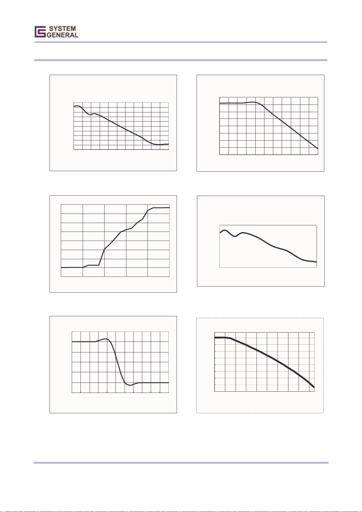
Min. Operating Voltage (V
DD(min)
) vs
Tempe r ature
10.20
10.15
10.10
10.05
(V)
10.00
9.95
9.90
DD(min)
V
9.85
9.80
9.75
9.70
-40 -25 -10 5 20 35 50 65 8 0 95 110 125
TEMPERATURE (
14
12
10
8
6
Ton (uS)
4
2
0
-2
0.620 0.628 0.636 0.644 0.652 0.660
RT Voltage vs Ton
RT VOLTAGE (V)
)
℃℃℃℃
Start Threshold Volta ge (V
TH(ON)
Temperature
16.6 0
16.5 5
16.5 0
16.4 5
(V)
16.4 0
TH(ON)
16.3 5
V
16.3 0
16.2 5
16.2 0
-40 -25 -10 5 2035 5065 80 95110 125
TEMPERATURE (
)
℃℃℃℃
Output Curre nt of pin R T (IRT) vs
Temperature
101.5
101.0
100.5
100.0
(uA)
RT
I
99.5
99.0
98.5
-40 -25 -10 5 20 35 50 65 80 95 110 125
TEMPERATURE (℃℃℃℃)
) vs
V
0.63
0.62
0.62
(V)
0.61
OTP, STOP
0.61
V
0.60
0.60
-40 -25 -10 5 20 35 50 65 80 95 110 125
vs Temperature
OTP, STOP
TEMPERATURE (
)
℃℃℃℃
0.84
0.79
0.74
0.69
SENSE
0.64
V
0.59
0.54
0.49
0.44
04080120 16 0 200 240 280 32 0 3 60
V
SENSE
I
VIN
vs I
(uA)
VIN
©System General Corp. - 8 - www.sg.com.tw
Version 1.7 (IRO33.0001.B1) JUL.25,2003
Page 9

Product Specification
High-integrated Green-mode PWM Controller SG6841
OPERATION DESCRIPTION
Start-up current
Typical start-up current is only 30uA so that a high
resistance, and low-wattage, start-up resistor can be used
to minimize power loss. For an AC/DC adapter with
universal input range, a 1.5 MΩ, 0.25W, start-up resistor
and a 10uF/25V VDD hold-up capacitor are enough for
this application.
Operating current
Operating current has been reduced to 3mA. The low
operating current enables a better efficiency and reduces
the requirement of VDD hold-up capacitance.
Green Mode Operation
The patented green-mode function provides an
off-time modulation to reduce the switching frequency in
the light load and no load conditions. The on time is
limited for better abnormal or brownout protection. V
,
FB
which is derived from the voltage feedback loop, is taken
as the reference. Once V
is lower than the threshold
FB
voltage, switching frequency will be linearly decreased to
the minimum green mode frequency around 10kHz (R
i
=26kΩ).
Oscillator Operation
A resistor from RI pin to ground will generate a
constant current source for SG6841. This current is used
to charge an internal capacitor and hence the internal
clock and switching frequency are determined. Increase
the resistance will decrease the current source and reduce
the switching frequency. A 26kΩ resistor R
50uA constant current I
and generates 65kHz switching
i
creates a
i
frequency. The relation between Ri and switching
freauency is:
1690
=
f
PWM
I
Ω
The range of the PWM oscillation frequency is
designed as 50kHz ~ 90kHz.
)(kHz
---------------------------- (1)
)(kR
Current sensing and PWM current
limiting
Peak current mode control is utilized in SG6841 to
regulate output voltage and provide pulse by pulse current
limiting. The switch current is detected by a sense resistor
into the sense pin of SG6841. The PWM duty cycle is
determined by this current sense signal and V
, the
FB
feedback voltage. When the voltage on sense pin reaches
V
= (VFB–1.0)/3, a switch cycle will be terminated
COMP
immediately. V
is internally clamped to a variable
COMP
voltage around 0.85v for output power limit.
Leading Edge Blanking
Each time when the power MOSFET is switched on,
a turn-on spike will inevitably occur on the sense-resistor.
To avoid premature termination of the switching pulse, a
270 nsec leading-edge blanking time is built in.
Conventional RC filtering can therefore be omitted.
During this blanking period, the current-limit comparator
is disabled and it cannot switch off the gate driver.
Under-voltage lockout (UVLO)
The turn-on and turn-off threshold of SG6841 are
fixed internally at 16V/10V. During start-up, the hold-up
capacitor must be charged to 16V through the start-up
resistor so that SG6841 will be enabled. The hold-up
capacitor will continue to supply V
before the energy
DD
can be delivered from auxiliary winding of the main
transformer. V
must not drop below 10V during this
DD
start-up process. This UVLO hysteresis window insures
that hold-up capacitor is adequate to supply V
during
DD
start-up.
Gate Output / Soft Driving
The SG6841 BiCMOS output stage is a fast totem
pole gate driver. Cross conduction has been avoided to
minimize heat dissipation, increases efficiency and
enhances reliability. The output driver is clamped by an
internal 18V Zener diode in order to protect power
MOSFET transistors against undesirable gate over
voltage. A soft driving waveform is implemented to
minimize EMI.
©System General Corp. - 9 - www.sg.com.tw
Version 1.7 (IRO33.0001.B1) JUL.25,2003
Page 10

Product Specification
High-integrated Green-mode PWM Controller SG6841
Built-in Slope Compensation
The sensed voltage across the current sense resistor
is used for current mode control and pulse-by-pulse
current limiting. Built-in slope compensation will
improve stability or prevent sub-harmonic oscillation of
peak current mode control. SG6841 inserts a
At high ambient temperature, Rntc will be smaller
such that V
(V
OTP,START
will decrease. When VRT is less than 0.65V
RT
), the PWM duty cycle will be decreased to
lower the internal temperature of power supply. If the
over heating situation still exists such that V
further to 0.62V (V
), the PWM will be completely
OTP,STOP
decreases
RT
turned off.
synchronized positive-going ramp at every switching
cycle. Vs-comp = 0.33V.
Limited Power Control
Const ant Output Power Limit
When the SENSE voltage, across the sense resistor
Rs, reaches the threshold voltage, around 1.0V, the output
GATE drive will be turned off after a small propagation
delay t
additional current proportional to t
propagation delay is nearly constant regardless of the
input line voltage V
in a larger additional current and hence the output power
limit is also higher than that under low input line voltage.
To compensate this variation for wide AC input range, the
threshold voltage is adjusted by the V
VIN pin is connected to the rectified input line voltage
through the start-up resistor, a higher line voltage will
generate higher V
threshold voltage is decreased if the V
increased. Smaller threshold voltage, forces the output
GATE drive to terminate earlier, thus reduce the total
PWM turn-on time and make the output power equal to
that of low line input. This proprietary internal
compensation ensures a constant output power limit for
wide AC input voltage from 90VAC to 264VAC.
. This propagation delay will introduce an
D
*Vin/Lp. Since the
D
Higher input line voltage will result
IN.
current. Since
IN
current into the VIN pin. The
IN
current is
IN
Every time when the output of power supply is
shorted or over loaded, the FB voltage will increase. If the
FB voltage is higher than a designed threshold, 4.2V, for
longer than 31msec, the PWM output will then be turned
off eternally. V
decrease due to the supply current for SG6841. When V
, the supply voltage for SG6841, will
DD
DD
is lower than the turn-off threshold such as 10V, SG6841
will be totally shut down. Due to the start up resistor, V
DD
will be charged up to the turn-on threshold voltage 16V
until SG6841 is enabled again. If the over loading
condition still exists, above protection will take place
repeatedly. This will prevent the power supply from being
overheated under over loading condition.
Noise immunity
Noise on the current sense or control signal may
cause significant pulse width jitter, particularly in the
continuous conduction mode. Slope compensation helps
alleviate this problem. Good placement and layout
practices should be followed. Avoiding long PCB traces
and component leads, locating compensation and filter
components near to the SG6841, and increasing the power
MOS gate resistance will always help.
Thermal Protection
An NTC thermistor Rntc in series with a resistor Ra
can be connected from pin RT to ground. A constant
current I
can be expressed as V
2 x (1.3V / Ri).
©System General Corp. - 10 - www.sg.com.tw
Version 1.7 (IRO33.0001.B1) JUL.25,2003
is output from pin RT. The voltage on RT pin
RT
= IRT × (Rntc + Ra) in which IRT =
RT
Page 11
Product Specification
High-integrated Green-mode PWM Controller SG6841
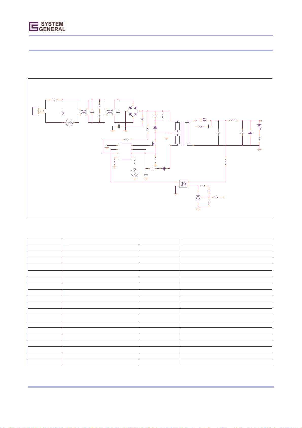
REFERENCE CIRCUIT
Circuit
F1
2
C2
SG6841
4
R7
GATE
VDD
SENSE
THER2
BD1
1
R3
3
C4
R5
8
7
6
1
R10
R12
+
C9
1 2
D2
2 1
23
Q2
R8
D4
1,2
1,2
3
3
4
4
5 6,7
5 6,7
21
U2
4
C3
+
Q1
1
8,9
3 2
8,9
R4
C6
C7
1
23
R13
3
C10
R14
1
U3
R15
2
L3
1 2
+
R11
Vo+
+
C8
Vo+
21
D1
D3
2 1
R6
CN1
1
2
3
12
VZ1
THER1
1 2
3 4
L1
1 2
R1
3 4
L2
C1
1 2
R2
C5
U1
1
GND
2
FB
3
VIN
4 5
RI RT
R9
BOM
Reference Component Reference Component
BD1 BD 4A/600V R1,R2 R 1Mohm 1/4W
C1 XC 0.1uF/275V R3 R 100Kohm 1/2W
C2 XC 0.22uF/275V R4 R 47ohm 1/4W
C3 CC 0.01uF/500V R5,R7 R 750Kohm 1/4W
C4 EC 120u/400V R6 R 20Kohm 1/8W
C5 YC 222p/Y1 R8 R 0.3ohm 2W
C6 CC 1000pF/100V R9 R 33Kohm 1/ 8W
C7 CC 1000pF/50V R9 R 20Kohm 1/8W 1%
C8 EC 1000uF/35V R11 R 220ohm 1/8W
C9 EC 220uF/35V R12 R 4.7ohm 1/8W
D1 LED R13 R 6.8Kohm 1/8W
D2 Diode FR157 R14 R 154Kohm 1/8W
D3 ZD 18V R15 R 390Kohm 1/8W
D4 Diode FR102 THER1 Thermist or SCK054
F1 FUSE 4A/250V T1 Transformer
L1 900uH U1 IC SG6841
L2 15mH U2 IC PC817
Q1 Diode 20A100V U3 IC TL431
Q2 MOS 7A/600V VZ1 VZ 9G
©System General Corp. - 11 - www.sg.com.tw
Version 1.7 (IRO33.0001.B1) JUL.25,2003
Page 12
Product Specification
High-integrated Green-mode PWM Controller SG6841
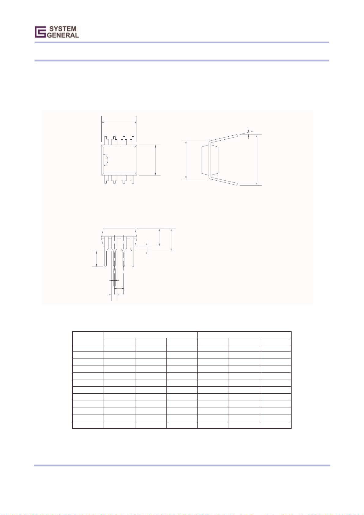
PACKAGE INFORMATION
8 PINS– DIP (D)
D
°
85
Θ
Dimension
E1
41
A2
A1
L
b1
e
b
E
A
eB
Symbol
A 5.334 0.210
A1 0.381 0.015
A2 3.175 3.302 3.429 0.125 0.130 0.135
b 1.524 0.060
b1 0.457 0.018
D 9.017 9.271 10.160 0.355 0.365 0.400
E 7.620 0.300
E1 6.223 6.350 6.477 0.245 0.250 0.255
e 2.540 0.100
L 2.921 3.302 3.810 0.115 0.130 0.150
eB 8.509 9.017 9.525 0.335 0.355 0.375
θ˚˚˚˚ 0˚˚˚˚ 7˚˚˚˚ 15˚˚˚˚ 0˚˚˚˚ 7˚˚˚˚ 15˚˚˚˚
Min. Typ. Max. Min. Typ. Max.
©System General Corp. - 12 - www.sg.com.tw
Version 1.7 (IRO33.0001.B1) JUL.25,2003
Page 13
Product Specification
High-integrated Green-mode PWM Controller SG6841
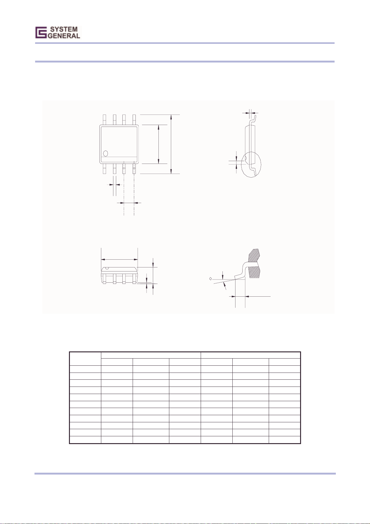
8 PINS– SOP (S)
85
E
1
4
b
e
D
A
A1
C
H
F
Θ
L
Dimension
Symbol
A 1.346 1.752 0.053 0.069
A1 0.101 0.254 0.004 0.010
b 0.406 0.016
c 0.203 0.008
D 4.648 4.978 0.183 0.196
E 0.381 3.987 0.150 0.157
e 1.270 0.050
F
H 5.791 6.197 0.228 0.244
L 0.406 1.270 0.016 0.050
θ˚˚˚˚ 0˚˚˚˚ 8˚˚˚˚ 0˚˚˚˚ 8˚˚˚˚
©System General Corp. - 13 - www.sg.com.tw
Version 1.7 (IRO33.0001.B1) JUL.25,2003
Min. Typ. Max. Min. Typ. Max.
Page 14

Product Specification
High-integrated Green-mode PWM Controller SG6841
DISCLAIMERS
LIFE SUPPORT
System General’s products are not designed to be used as components in devices intended to support or sustain
human life. Use of System General’s products in components intended for surgical implant into the body, or other
applications in which failure of the System General’s products could create a situation where personal death or injury may
occur, is not authorized without the express written approval of System General’s Chief Executive Officer. System
General will not be held liable for any damages or claims resulting from the use of its products in medical applications.
MILITARY
System General's products are not designed for use in military applications. Use of System General’s products in
military applications is not authorized without the express written approval of System General’s Chief Executive Officer.
System General will not be held liable for any damages or claims resulting from the use of its products in military
applications.
RIGHT TO MAKE CHANGES
System General reserves the right to change this document and/or this product without notice. Customers are advised
to consult their System General sales representative before ordering.
©System General Corp. - 14 - www.sg.com.tw
Version 1.7 (IRO33.0001.B1) JUL.25,2003
 Loading...