

Page 1
Order this document by SG3525A/D
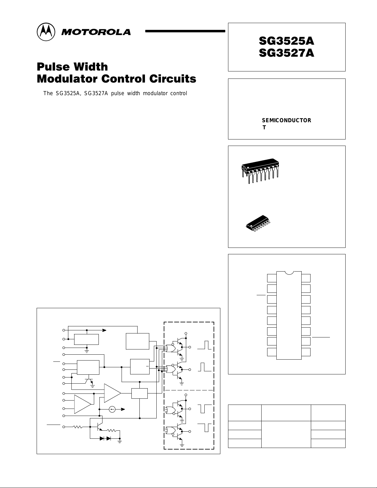
The SG3525A, SG3527A pulse width modulator control circuits offer
improved performance and lower external parts count when implemented for
controlling all types of switching power supplies. The on–chip +5.1 V
reference is trimmed to ±1% and the error amplifier has an input
common–mode voltage range that includes the reference voltage, thus
eliminating the need for external divider resistors. A sync input to the
oscillator enables multiple units to be slaved or a single unit to be
synchronized to an external system clock. A wide range of deadtime can be
programmed by a single resistor connected between the CT and Discharge
pins. These devices also feature built–in soft–start circuitry , requiring only an
external timing capacitor. A shutdown pin controls both the soft–start circuitry
and the output stages, providing instantaneous turn off through the PWM
latch with pulsed shutdown, as well as soft–start recycle with longer
shutdown commands. The under voltage lockout inhibits the outputs and the
changing of the soft–start capacitor when VCC is below nominal. The output
stages are totem–pole design capable of sinking and sourcing in excess of
200 mA. The output stage of the SG3525A features NOR logic resulting in a
low output for an off–state while the SG3527A utilized OR logic which gives a
high output when off.
• 8.0 V to 35 V Operation
• 5.1 V ± 1.0% Trimmed Reference
• 100 Hz to 400 kHz Oscillator Range
• Separate Oscillator Sync Pin
• Adjustable Deadtime Control
• Input Undervoltage Lockout
• Latching PWM to Prevent Multiple Pulses
• Pulse–by–Pulse Shutdown
• Dual Source/Sink Outputs: ±400 mA Peak
Representative Block Diagram
V
ref
V
CC
Ground
OSC Output
Sync
RT
CT
Discharge
Compensation
INV. Input
Noninv. Input
C
Soft–Start
Shutdown
16
15
12
Reference
Regulator
4
3
6
Oscillator
5
7
9
1
–
Error
2
Amp
+
8
5.0k
10
T o Internal
Circuitry
+
– PWM
–
50
µ
5.0k
Under–
Voltage
Lockout
Q
F/F
Q
R
S
Latch
V
S
REF
A
VC
13
Output A
NOR
NOR
SG3525A Output Stage
OR
OR
11
14
Output B
13
VC
Output A
11
Output B
14
SG3527A
Output Stage
PULSE WIDTH MODULATOR
CONTROL CIRCUITS
SEMICONDUCTOR
TECHNICAL DATA
N SUFFIX
16
1
16
1
Inv. Input
Noninv. Input
OSC. Output
Discharge
Soft–Start
ORDERING INFORMATION
Device
SG3525AN
SG3525ADW
SG3527AN
PIN CONNECTIONS
1
2
Sync
3
4
C
5
T
R
6
T
7
89
Temperature Range
TA = 0° to +70°C
PLASTIC PACKAGE
DW SUFFIX
PLASTIC PACKAGE
CASE 751B
(Top View)
Operating
CASE 648
(SO–16L)
V
16
ref
V
15
CC
Output B
14
V
13
C
Ground
12
Output A
11
Shutdown
10
Compensation
Package
Plastic DIP
SO–16L
Plastic DIP
MOTOROLA ANALOG IC DEVICE DATA
Motorola, Inc. 1996 Rev 2
1
Page 2

SG3525A SG3527A
MAXIMUM RATINGS
Supply Voltage V
Collector Supply Voltage V
Logic Inputs –0.3 to +5.5 V
Analog Inputs –0.3 to V
Output Current, Source or Sink I
Reference Output Current I
Oscillator Charging Current 5.0 mA
Power Dissipation (Plastic & Ceramic Package)
TA = +25°C (Note 2)
TC = +25°C (Note 3)
Thermal Resistance Junction–to–Air R
Thermal Resistance Junction–to–Case R
Operating Junction Temperature T
Storage Temperature Range T
Lead Temperature (Soldering, 10 seconds) T
NOTES: 1.Values beyond which damage may occur.
2.Derate at 10 mW/°C for ambient temperatures above +50°C.
3.Derate at 16 mW/°C for case temperatures above +25°C.
(Note 1)
Rating Symbol Value Unit
CC
C
O
ref
P
D
θJA
θJC
J
stg
Solder
+40 Vdc
+40 Vdc
CC
±500 mA
50 mA
1000
2000
100 °C/W
60 °C/W
+150 °C
–55 to +125 °C
+300 °C
V
mW
RECOMMENDED OPERATING CONDITIONS
Characteristics Symbol Min Max Unit
Supply Voltage V
Collector Supply Voltage V
Output Sink/Source Current
(Steady State)
(Peak)
Reference Load Current I
Oscillator Frequency Range f
Oscillator Timing Resistor R
Oscillator Timing Capacitor C
Deadtime Resistor Range R
Operating Ambient Temperature Range T
APPLICATION INFORMATION
Shutdown Options (See Block diagram, front page)
Since both the compensation and soft–start terminals
(Pins 9 and 8) have current source pull–ups, either can
readily accept a pull–down signal which only has to sink a
maximum of 100 µA to turn off the outputs. This is subject to
the added requirement of discharging whatever external
capacitance may be attached to these pins.
An alternate approach is the use of the shutdown circuitry
of Pin 10 which has been improved to enhance the available
shutdown options. Activating this circuit by applying a
positive signal on Pin 10 performs two functions: the PWM
latch is immediately set providing the fastest turn–off signal to
the outputs; and a 150 µA current sink begins to discharge
the external soft–start capacitor. If the shutdown command is
short, the PWM signal is terminated without significant
discharge of the soft–start capacitor, thus, allowing, for
example, a convenient implementation of pulse–by–pulse
current limiting. Holding Pin 10 high for a longer duration,
however, will ultimately discharge this external capacitor,
recycling slow turn–on upon release.
Pin 10 should not be left floating as noise pickup could
conceivably interrupt normal operation.
CC
I
O
ref
osc
8.0 35 Vdc
C
T
T
D
A
4.5 35 Vdc
0
0
0 20 mA
0.1 400 kHz
2.0 150 kΩ
0.001 0.2 µF
0 500 Ω
0 +70 °C
±100
±400
mA
2
MOTOROLA ANALOG IC DEVICE DATA
Page 3

SG3525A SG3527A
ELECTRICAL CHARACTERISTICS (V
Characteristics
= +20 Vdc, TA = T
CC
low
to T
[Note 4], unless otherwise noted.)
high
Symbol Min Typ Max Unit
REFERENCE SECTION
Reference Output Voltage (TJ = +25°C) V
Line Regulation (+8.0 V ≤ VCC ≤ +35 V) Reg
Load Regulation (0 mA ≤ IL ≤ 20 mA) Reg
T emperature Stability ∆V
Total Output Variation
∆V
Includes Line and Load Regulation over Temperature
Short Circuit Current
(V
= 0 V, TJ = +25°C)
ref
Output Noise Voltage (10 Hz ≤ f ≤ 10 kHz, TJ = +25°C) V
ref
line
load
/∆T – 20 – mV
ref
ref
I
SC
n
5.00 5.10 5.20 Vdc
– 10 20 mV
– 20 50 mV
4.95 – 5.25 Vdc
– 80 100 mA
– 40 200 µV
Long Term Stability (TJ = +125°C) (Note 5) S – 20 50 mV/khr
OSCILLATOR SECTION (Note 6, unless otherwise noted.)
Initial Accuracy (TJ = +25°C) – ±2.0 ±6.0 %
Frequency Stability with Voltage
(+8.0 V ≤ VCC ≤ +35 V)
Frequency Stability with Temperature
Minimum Frequency (RT = 150 kΩ, CT = 0.2 µF) f
Maximum Frequency (RT = 2.0 kΩ, CT = 1.0 nF) f
∆f
D
∆f
osc
VCC
osc
D
min
max
– ±1.0 ±2.0 %
– ±0.3 – %
T
– 50 – Hz
400 – – kHz
Current Mirror (IRT = 2.0 mA) 1.7 2.0 2.2 mA
Clock Amplitude 3.0 3.5 – V
Clock Width (TJ = +25°C) 0.3 0.5 1.0 µs
Sync Threshold 1.2 2.0 2.8 V
Sync Input Current (Sync Voltage = +3.5 V) – 1.0 2.5 mA
ERROR AMPLIFIER SECTION (VCM = +5.1 V)
Input Offset Voltage V
Input Bias Current I
Input Offset Current I
DC Open Loop Gain (RL ≥ 10 MΩ) A
Low Level Output Voltage V
High Level Output Voltage V
IO
IB
IO
VOL
OL
OH
– 2.0 10 mV
– 1.0 10 µA
– – 1.0 µA
60 75 – dB
– 0.2 0.5 V
3.8 5.6 – V
Common Mode Rejection Ratio (+1.5 V ≤ VCM ≤ +5.2 V) CMRR 60 75 – dB
Power Supply Rejection Ratio (+8.0 V ≤ VCC ≤ +35 V) PSRR 50 60 – dB
PWM COMPARATOR SECTION
Minimum Duty Cycle DC
Maximum Duty Cycle DC
Input Threshold, Zero Duty Cycle (Note 6) V
Input Threshold, Maximum Duty Cycle (Note 6) V
Input Bias Current I
NOTES: 4.T
= 0° for SG3525A, 3527A T
low
5.Since long term stability cannot be measured on each device before shipment, this specification is an engineering estimate of average stability
from lot to lot.
6.Tested at f
= 40 kHz (RT = 3.6 kΩ, CT = 0.01 µF, RD = 0Ω).
osc
= +70°C for SG3525A, 3527A
high
min
max
th
th
IB
– – 0 %
45 49 – %
0.6 0.9 – V
– 3.3 3.6 V
– 0.05 1.0 µA
rms
MOTOROLA ANALOG IC DEVICE DATA
3
Page 4

SG3525A SG3527A
ELECTRICAL CHARACTERISTICS (Continued)
Characteristics Symbol Min Typ Max Unit
SOFT–START SECTION
Soft–Start Current (V
Soft–Start Voltage (V
Shutdown Input Current (V
OUTPUT DRIVERS (Each Output, VCC = +20 V)
Output Low Level
(I
= 20 mA)
sink
(I
= 100 mA)
sink
Output High Level
(I
= 20 mA)
source
(I
= 100 mA)
source
Under Voltage Lockout (V8 and V9 = High) V
Collector Leakage, VC = +35 V (Note 7) I
Rise Time (CL = 1.0 nF, TJ = 25°C) t
Fall Time (CL = 1.0 nF, TJ = 25°C) t
Shutdown Delay (VDS = +3.0 V, CS = 0, TJ = +25°C) t
Supply Current (VCC = +35 V) I
NOTE: 7.Applies to SG3525A only , due to polarity of output pulses.
shutdown
shutdown
= 0 V) 25 50 80 µA
= 2.0 V) – 0.4 0.6 V
shutdown
= 2.5 V) – 0.4 1.0 mA
V
OL
V
OH
UL
C(leak)
r
f
ds
CC
–
–
18
17
6.0 7.0 8.0 V
– – 200 µA
– 100 600 ns
– 50 300 ns
– 0.2 0.5 µs
– 14 20 mA
0.2
1.0
19
18
0.4
2.0
–
–
V
V
PWM
ADJ.
V/I Meter
V
3.0k
1.0k
1.5k
ref
–
+
0.009
0.1
Clock
Sync
1 = V
IO
2 = 1(+)
3 = 1(–)
1
2
3
1
2
3
RT
Ramp
2
Deadtime
0.001
10k
1
2
3
1
3
100
Ω
0.01
0.1
Comp
16
Lab T est Fixture
Reference Regulator
4
3
6
7
5
9
1
2
O
s
c
i
l
l
a
t
o
r
–
E/A
+
DUT
Flip/
Flop
PWM
50
5.0k
A
B
µ
A
5.0k
15
13
11
1.0k, 1.0W
14
12
8
10
(2)
0.1
+
0.1
Out A
Out B
5.0
2.0k
V
CC
V
C
Gnd
Softstart
µ
F
Shutdown
V
ref
4
MOTOROLA ANALOG IC DEVICE DATA
Page 5

SG3525A SG3527A
Figure 1. Oscillator Charge Time versus R
200
100
Ω
50
20
10
, TIMING RESISTOR (k )
5.0
T
R
6
R
2.0
2.0 5.0 10 20 50 100 200 500 1000 2000 5000 10,000
CHARGE TIME (
µ
s)
Figure 3. Error Amplifier Open Loop
Frequency Response
1
–
+
2
100
80
60
40
, VOLTAGE GAIN (dB)
20
VOL
A
0
–20
1.0 10 100 1.0 k 10 k 100 k 1.0 M 10 M
f, FREQUENCY (Hz)
RZ = 20 k
T
* RD = 0
Ω
57
R
*
D
T
C
T
9
C
P
R
Z
Figure 2. Oscillator Discharge Time versus R
500
Ω
400
300
200
, DEAD TIME RESISTOR ( )
D
100
R
0
0.2 0.5 1.0 2.0 5.0 10 20 50 100 200
DISCHARGE TIME (
µ
s)
Figure 4. Output Saturation
Characteristics (SG3525A)
VCC = +20 V
°
C
TJ = +25
Source Sat, (VC–VOH)
Sink Sat, (VOL)
0
0.01 0.02 0.03 0.05 0.07 0.1 0.2 0.3 0.5 0.7 1.0
IO, OUTPUT SOURCE OR SINK CURRENT (A)
, SATURATION VOLTAGE (V)
sat
V
4.0
3.5
3.0
2.5
2.0
1.5
1.0
0.5
D
Figure 5. Oscillator Schematic (SG3525A)
V
ref
16
R
T
6
C
T
5
3
Sync
7
Discharge
Q2
12
Q1
Q4
1.0k
Q3
5.0pF
Q7
Q5 Q8
Q6 Q9
2.0k
400
µ
A
23k
2.0k 14k
Q10
1.0k
7.4k
Q11
Q12
Gnd
MOTOROLA ANALOG IC DEVICE DATA
25k
Q14
Q13
3.0k
Ramp
To PWM
Blanking
To Output
250
4
OSC Output
Figure 6. Error Amplifier Schematic (SG3525A)
15
V
CC
Q3
100
Q4
µ
A
5.8V
930Compensation
Inverting
Input
1
Noninverting
Input
2
200µA
Q1 Q2
To PWM
Comparator
5
Page 6

SG3525A SG3527A
Figure 7. SG3525A Output Circuit
(1/2 Circuit Shown)
V
CC
Q7
Q9
5.0k
Q8
Q6
2.0k
Q4
Q5
V
ref
Q10
Q11
13
Output
V
C
11, 14
Q1 Q2
5.0k 10k 10k
Clock F/F PWM
Q3
Q6 Omitted
in SG3527A
Figure 8. Single–Ended Supply Figure 9. Push–Pull Configuration
Q1
V
C
Gnd
R2
13
12
To Output Filter
11
A
14
B
+Vsupply
R1
SG3525A
For single–ended supplies, the driver outputs are grounded.
The VC terminal is switched to ground by the totem–pole
source transistors on alternate oscillator cycles.
+V
supply
R1
11
14
C1
R2
C2
R3
Q1
Q2
13
V
C
A
SG3525A
B
Gnd
12
In conventional push–pull bipolar designs, forward base drive is
controlled by R1–R3. Rapid turn–off times for the power
devices are achieved with speed–up capacitors C1 and C2.
T1
Figure 10. Driving Power FETS
+Vsupply
The low source impedance of the output drivers provides
rapid charging of power FET input capacitance while
minimizing external components.
R1
13
V
C
SG3525A
Gnd
12
Q1
11
A
Q2
14
B
6
T1
Figure 11. Driving Transformers in a
Half–Bridge Configuration
+V
supply
T1
13
11
V
A
C
SG3525A
Low power transformers can be driven directly by the SG3525A.
Automatic reset occurs during deadtime, when both ends of the
primary winding are switched to ground.
Gnd
12
14
B
Q1
Q2
R1
R2
C1
T2
C2
MOTOROLA ANALOG IC DEVICE DATA
Page 7

–T–
SG3525A SG3527A
OUTLINE DIMENSIONS
N SUFFIX
PLASTIC PACKAGE
CASE 648–08
–A–
916
B
18
F
C
S
–T–
H
G
D
16 PL
0.25 (0.010) T
K
M
A
–A–
16 9
–B–
18
8 PLP
G
K
C
SEATING
PLANE
D
16 PL
0.25 (0.010) A
M
S
B
T
S
ISSUE R
SEATING
PLANE
M
DW SUFFIX
PLASTIC PACKAGE
CASE 751B–05
(SO–16L)
ISSUE J
0.25 (0.010) B
M
NOTES:
1. DIMENSIONING AND TOLERANCING PER ANSI
Y14.5M, 1982.
2. CONTROLLING DIMENSION: INCH.
3. DIMENSION L TO CENTER OF LEADS WHEN
FORMED PARALLEL.
4. DIMENSION B DOES NOT INCLUDE MOLD FLASH.
5. ROUNDED CORNERS OPTIONAL.
DIM MIN MAX MIN MAX
L
J
M
S
R
X 45
M
_
F
J
A 0.740 0.770 18.80 19.55
B 0.250 0.270 6.35 6.85
C 0.145 0.175 3.69 4.44
D 0.015 0.021 0.39 0.53
F 0.040 0.70 1.02 1.77
G 0.100 BSC 2.54 BSC
H 0.050 BSC 1.27 BSC
J 0.008 0.015 0.21 0.38
K 0.110 0.130 2.80 3.30
L 0.295 0.305 7.50 7.74
M 0 10 0 10
S 0.020 0.040 0.51 1.01
NOTES:
1. DIMENSIONING AND TOLERANCING PER
ANSI Y14.5M, 1982.
2. CONTROLLING DIMENSION: MILLIMETER.
3. DIMENSIONS A AND B DO NOT INCLUDE
MOLD PROTRUSION.
4. MAXIMUM MOLD PROTRUSION 0.15 (0.006)
PER SIDE.
5. DIMENSION D DOES NOT INCLUDE DAMBAR
PROTRUSION. ALLOWABLE DAMBAR
PROTRUSION SHALL BE 0.127 (0.005) TOTAL
IN EXCESS OF THE D DIMENSION AT
MAXIMUM MATERIAL CONDITION.
DIM MIN MAX MIN MAX
A 9.80 10.00 0.386 0.393
B 3.80 4.00 0.150 0.157
C 1.35 1.75 0.054 0.068
D 0.35 0.49 0.014 0.019
F 0.40 1.25 0.016 0.049
G 1.27 BSC 0.050 BSC
J 0.19 0.25 0.008 0.009
K 0.10 0.25 0.004 0.009
M 0 7 0 7
P 5.80 6.20 0.229 0.244
R 0.25 0.50 0.010 0.019
MILLIMETERSINCHES
____
INCHESMILLIMETERS
____
MOTOROLA ANALOG IC DEVICE DATA
7
Page 8

SG3525A SG3527A
Motorola reserves the right to make changes without further notice to any products herein. Motorola makes no warranty , representation or guarantee regarding
the suitability of its products for any particular purpose, nor does Motorola assume any liability arising out of the application or use of any product or circuit, and
specifically disclaims any and all liability, including without limitation consequential or incidental damages. “T ypical” parameters which may be provided in Motorola
data sheets and/or specifications can and do vary in different applications and actual performance may vary over time. All operating parameters, including “Typicals”
must be validated for each customer application by customer’s technical experts. Motorola does not convey any license under its patent rights nor the rights of
others. Motorola products are not designed, intended, or authorized for use as components in systems intended for surgical implant into the body, or other
applications intended to support or sustain life, or for any other application in which the failure of the Motorola product could create a situation where personal injury
or death may occur. Should Buyer purchase or use Motorola products for any such unintended or unauthorized application, Buyer shall indemnify and hold Motorola
and its officers, employees, subsidiaries, affiliates, and distributors harmless against all claims, costs, damages, and expenses, and reasonable attorney fees
arising out of, directly or indirectly, any claim of personal injury or death associated with such unintended or unauthorized use, even if such claim alleges that Motorola
was negligent regarding the design or manufacture of the part. Motorola and are registered trademarks of Motorola, Inc. Motorola, Inc. is an Equal
Opportunity/Affirmative Action Employer.
How to reach us:
USA/EUROPE /Locations Not Listed: Motorola Literature Distribution; JAPAN: Nippon Motorola Ltd.; Tatsumi–SPD–JLDC, 6F Seibu–Butsuryu–Center,
P.O. Box 20912; Phoenix, Arizona 85036. 1–800–441–2447 or 602–303–5454 3–14–2 Tatsumi Koto–Ku, Tokyo 135, Japan. 03–81–3521–8315
MFAX: RMF AX0@email.sps.mot.com – TOUCHT ONE 602–244–6609 ASIA/PACIFIC: Motorola Semiconductors H.K. Ltd.; 8B Tai Ping Industrial Park,
INTERNET: http://Design–NET .com 51 Ting Ko k Road, Tai Po, N.T., Hong Kong. 852–26629298
8
◊
MOTOROLA ANALOG IC DEVICE DATA
SG3525A/D
*SG3525A/D*
 Loading...