

Page 1
查询SG29125供应商
SG29125/125A
LOW DROPOUT DUAL REGULATOR
DESCRIPTION
The SG29125/125A is a dual 12V/5V positive voltage regulator. One output is a high
current (up to 1000 mA) regulator that can be turned on or off by a high impedance low
current TTL compatible switch. The second or standby output remains on regardless.
The on/off switch not only shuts off the high current output but actually puts the IC in
a micropower mode making possible a low quiescent current. This unique characteristic coupled with an extremely low dropout, (.55V for output current of 10mA) makes
the SG29125/125A well suited for power systems that require standby memory. The
SG29125/125A includes other features which were originally designed for automotive
applications. These include protection from reverse battery installations and double
battery jumps. The high current regulator has overvoltage shutdown to protect both
the internal circuitry and the load during line transients, such as load dump (60V). In
addition, the high current regulator design also has built-in protection for short circuit
and thermal overload. During these fault conditions of the primary regulator the
standby regulator will continue to power its load.
The SG29125 is the 12 volt, ±5% version of a family of dual regulators with a standby
output voltage of 5V. Other high current outputs of 5 and 8.2 volts are available. Also
available is the SG29125A which offers an improved output voltage tolerance of ±2%.
They are available in the plastic TO-220 power package and are designed to function
over the automotive ambient temperature range of -40°C to 85°C.
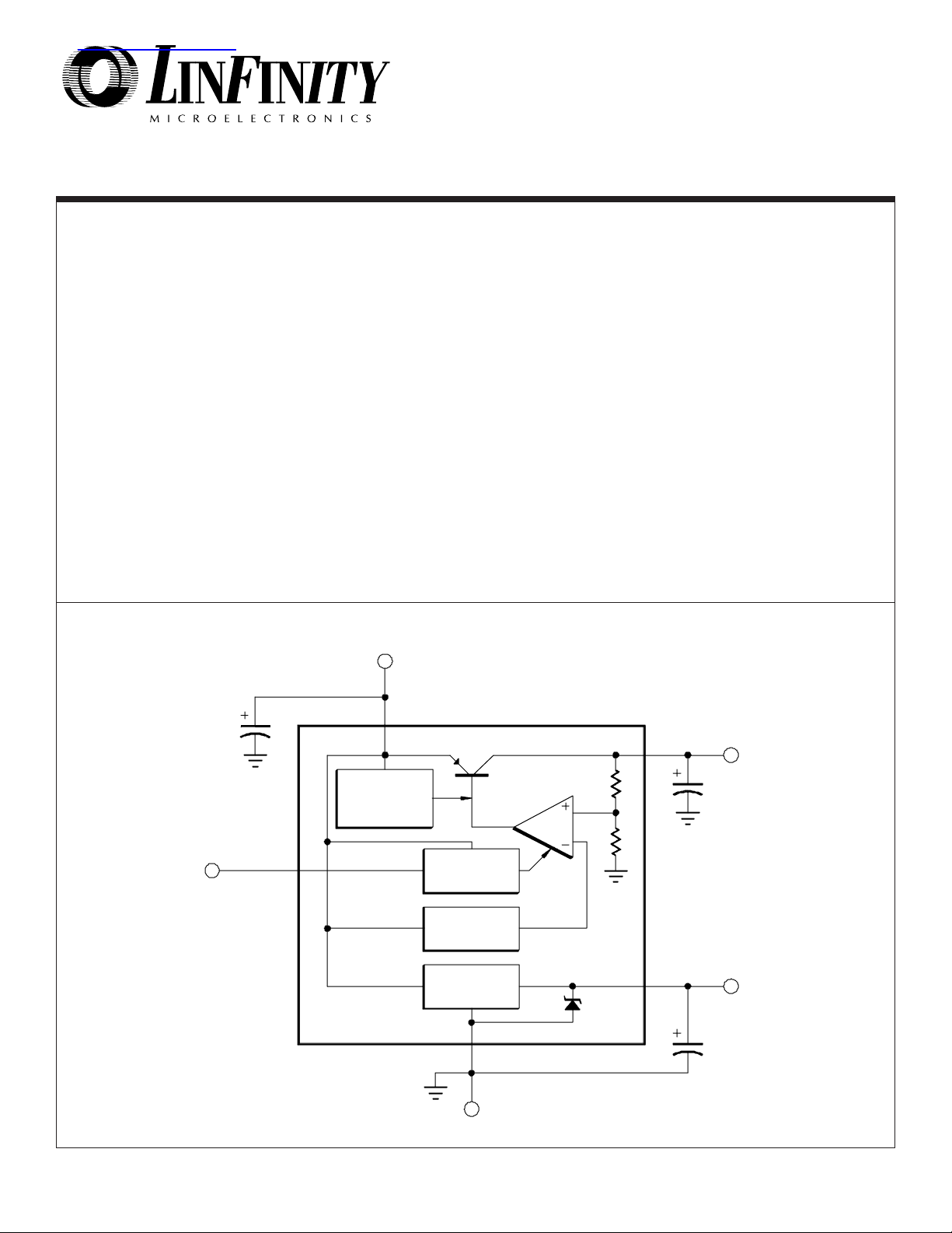
TYPICAL APPLICATION CIRCUIT
C1
*
0.1µF
INPUT VOLTAGE
1
OVERVOLTAGE
THERMAL
SHUTDOWN
SG29125/125A
* Required if regulator is located far from power
** Required for stability. May be increased without
FEATURES
••
• 2% Internally Trimmed Output
••
••
• Two regulated outputs
••
••
• Output current in excess of
••
1000mA
••
• Low quiescent current standby
••
regulator
••
• Input-output differential less than
••
0.6V at 0.5A
••
• Reverse battery protection
••
••
• 60V load dump protection
••
••
• -50V reverse transient protection
••
••
• Short circuit protection
••
••
• Internal thermal overload protec-
••
tion
••
• Available in plastic TO-220
••
••
• ON/OFF switch for high current
••
output
supply filter.
bound. Capacitor must be rated to operate at the
minimum temperature expected for the regulator
system.
2
C2
10µF
**
OUTPUT VOLTAGE
(12V, 1000mA)
ON/OFF SWITCH
(for output voltage only)
12/90 Rev 1.1 2/94 LINFINITY Microelectronics Inc.
Copyright 1994 11861 Western Avenue
4
REGULATOR
BIAS
1.23V
REFERENCE
5V STANDBY
REGULATOR
3
GROUND
5.6V
5
C3**
10µF
1 (714) 898-8121
STANDBY OUTPUT
(5V, 50mA)
∞ ∞
∞ Garden Grove, CA 92841
∞ ∞
∞∞
∞ FAX: (714) 893-2570
∞∞
Page 2
ABSOLUTE MAXIMUM RATINGS Note 1. Exceeding these values may destroy this part.
Input Voltage (VIN) Operating ..............................................
Input Voltage (V
ON/OFF Switch .......................................................
) Overvoltage Transient ..............
IN
-15V to 60V
-0.3V to V
26V
Storage Temperature Range (T
Operating Junction Temperature (T
IN
THERMAL DATA
SG29125/125A
) ..................
STG
) ..............................
J
-65°C to 150°C
150°C
P Package:
Thermal Resistance-
Junction to Case, θ
................ 4.0°C/W*
JT
Thermal Resistance-Junction to Ambient, θJA.............. 55°C/W
θθ
* =
θJT (Junction to Tab)
θθ
Note A. Junction Temperature Calculation: TJ = TA + (PD x θJA).
Note B. The above numbers for
θJC are maximums for the limiting
thermal resistance of the package in a standard mounting configuration. The θ
guidelines for the thermal performance of the device/pc-
numbers are meant to be
JA
board system. All of the above assume no ambient
airflow.
RECOMMENDED OPERATING CONDITIONS (Note 2 & 3)
Input Voltage (VIN) .....................................................
13V to 26V
ON/OFF Threshold Voltage
(V
Low Level, V
High Level, V
Load Current V
Maximum Line Transient (Load Dump) V
Input Capacitor (V
Note 2. Range over which the device is functional.
Note 3. During 60V load dump, VSB shall not be less than 4.75V at I
is OFF) ..................................
IL
OUT
(V
is ON) ....................................
IH
OUT
(with adequate heatsinking) .....
OUT
to GND) ...................................
IN
SB
5 to 1000mA
≤ 6V .......
0.8V max.
2.0V min.
60V max.
0.1 µF min.
Reverse Polarity D.C. Input Voltage (V
(V
≥ -0.6V, 16Ω load) ...........................................
O
Reverse Polarity Transient Input Voltage (V
(1% duty cycle, T ≤ 100ms, V
Output Capacitor with ESR of 1Ω max.
to GND & VSBto GND) ...................................
(V
OUT
Operating Ambient Temperature Range (T
SG29125/125A ...............................................
= 10mA.
OUT
O
)
IN
)
IN
≥ -9V, 16Ω load) ...
)
A
-40°C to 85°C
-15V max.
-50V max.
10µF min.
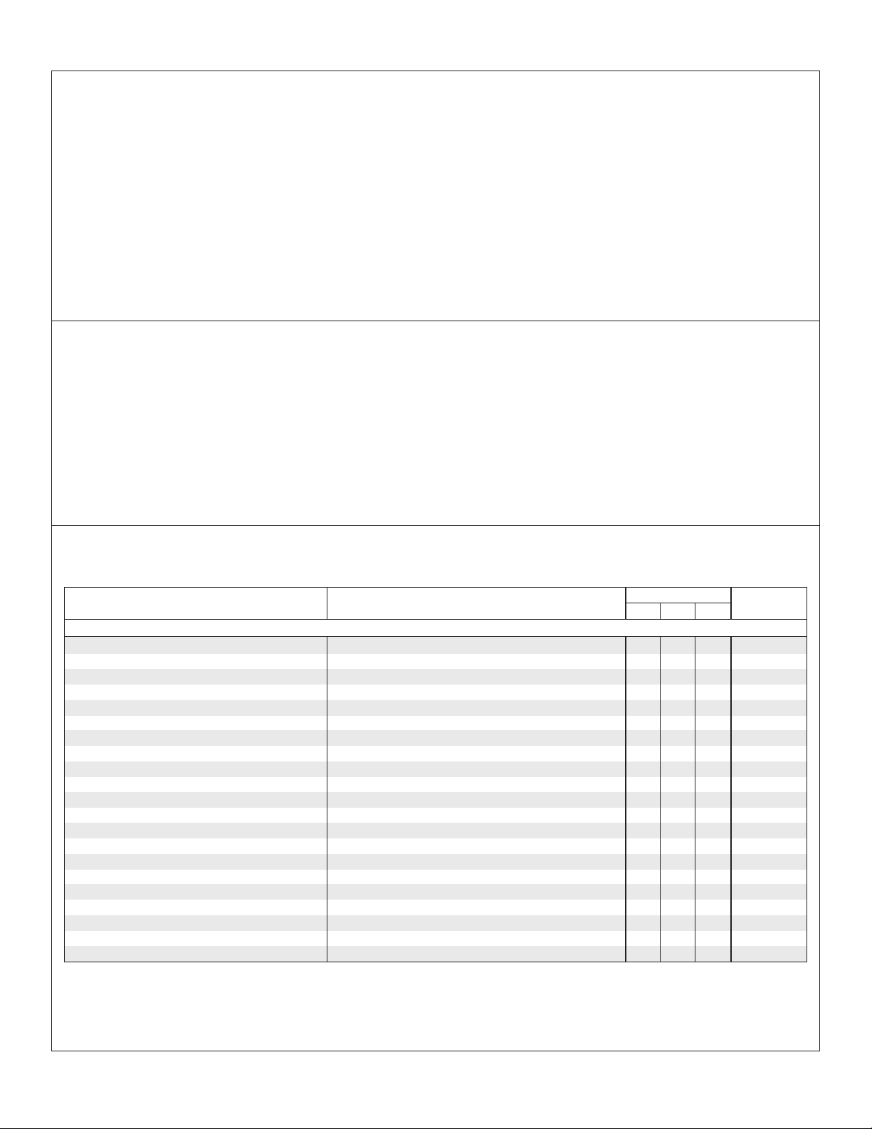
ELECTRICAL CHARACTERISTICS (Unless otherwise specified, these specifications apply for the operating ambient temperature of
= 25°C, VIN = 14V, IO = 500mA for V
T
A
maintains junction and case temperatures equal to the ambient temperature.)
Voltage Output (V
Output Voltage
OUT
(Note 4)
) Section
Line Regulation
Load Regulation
Output Impedance
Quiescent Current
Output Noise Voltage
Long Term Stability
Ripple Rejection
Dropout Voltage
Current Limit
Maximum Operational Input Voltage
Maximum Line Transient
ON/OFF Switch (I
ON/OFF Switch (I
)
IH
)
IL
and 10mA for VSB and are for DC characteristics only. Low duty cycle pulse testing techniques are used which
OUT
Test ConditionsParameter
13V ≤ V
SG29125
≤ 26V, IO ≤ 1000mA, -40°C ≤ TA ≤ 85°C
IN
SG29125A
13V ≤ V
13V ≤ V
5mA ≤ I
500mA
≤ 10mA, No Load on Standby
I
O
I
= 500mA, No Load on Standby
O
= 750mA, No Load on Standby
I
O
I
= 220mA, ISB = 10mA, VIN = V
O
10Hz - 100kHz
F
O
= 500mA
I
O
I
=1000mA
O
≤ 16V, IO = 5mA
IN
≤ 26V, IO = 5mA
IN
≤ 1000mA
O
and 10mA
DC
= 120Hz
, 100Hz - 10kHz
RMS
Double Battery
V
≤ 13V
O
= 10mA, Pin 4 = 2.4V
I
O
I
= 10mA, Pin 4 = 0.4V
O
- 200mV
OUT
SG29125/125A
Typ.
Min. Max.
11.2
12
12.8
11.75
12
10
10
12.25
4
25
50
50
200
2
40
100
90
15
25
100
20
66
0.45
0.6
.0.7
1.0
26.5
60
1.8
31
70
1.2
2.5
10
-10
Units
V
V
mV
mV
mV
mΩ
mA
mA
mA
mA
µV
mV/1000hr
dB
V
V
A
V
V
µA
µA
RMS
12/90 Rev 1.1 2/94 LINFINITY Microelectronics Inc.
Copyright 1994 11861 Western Avenue
2 (714) 898-8121
∞ ∞
∞ Garden Grove, CA 92841
∞ ∞
∞∞
∞ FAX: (714) 893-2570
∞∞
Page 3

ELECTRICAL CHARACTERISTICS (continued)
SG29125/125A
Test ConditionsParameter
Standby Output (V
Output Voltage (Note 4)
Line Regulation
Load Regulation
Output Impedance
Quiescent Current
Output Noise Voltage
) Section
SB
6V ≤ V
6V ≤ V
1mA ≤ I
1mA ≤ I
1mA
I
10Hz - 100kHz
≤ 26V, IO ≤ 50mA, -40°C ≤ TA ≤ 85°C
IN
≤ 26V
IN
≤ 35mA
O
≤ 50mA
O
and 1mA
DC
≤ 10mA, V
O
OUT
, 100Hz - 10kHz
RMS
OFF
Long Term Stability
F
Ripple Rejection
Dropout Voltage
Current Limit
Maximum Operational Input Voltage
Note 4. The temperature extremes are guaranteed but not 100% production tested.
TYPICAL CIRCUIT WAVEFORM
14V
INPUT
VOLTAGE
PIN 1 (V)
0V
60V
= 120Hz
O
I
≤ 50mA
O
4.75V ≤ V
33V
≤ 6V
O
26V
4V
SG29125/125A
Min. Max.
Typ.
4.75
5.0
5.25
4
50
10
25
25
50
1
1.2
3
300
20
66
0.55
0.7
50
100
60
70
14V
Units
V
mV
mV
mV
Ω
mA
µV
RMS
mV/1000hr
dB
V
mA
V
0.8V
2V
ON
12V
LOAD
DUMP
5V
0V
5V
TURN
12V
LOW V
3.5V
3.7V
IN
ON/OFF
SWITCH
OUTPUT
VOLTAGE
PIN 2 (V)
STANDBY
VOLTAGE
PIN 5 (V)
SYSTEM
CONDITION
APPLICATION NOTES
The advantages of using a low-dropout regulator such as the
SG29125/125A are the need for less “headroom” for full regulation, and the inherent reverse polarity protection provided by the
PNP output device. A typical NPN regulator design requires an
input to output differential of approximately two volts minimum.
This is due to the 2Vbe + Vcesat of the NPN Darlington used in
the output, coupled with the voltage drop across the current limit
resistor. In contrast, the “PNP Regulator” uses a single series
pass transistor with its single Vcesat, thus the lower input to
output voltage differential or dropout voltage.
In addition to a low dropout voltage, an important advantage of
the SG29125/125A series is low quiescent current in the standby
mode. When the high current or primary regulator is shut off, the
0.8V
12V12V
TURN
OFF
0V
LINE NOISE,
ETC.
12V
V
OUT
SHORT
CIRCUIT
5.0V
THERMAL
SHUTDOWN
regulator enters a micropower mode. Here all but the most
essential circuitry to power the standby output is deactivated.
This allows the lowest possible quiescent current (typical around
1.2mA), a vital factor when used in a battery powered system.
In some applications the regulator output voltage is used not only
as a power supply but also as a voltage reference for control
systems. In such cases not just the temperature stability of the
output is important but also the initial accuracy. The SG29125/
125A fills this need as the internal bandgap reference is trimmed
allowing a typical output voltage tolerance of ±1%.
12/90 Rev 1.1 2/94 LINFINITY Microelectronics Inc.
Copyright 1994 11861 Western Avenue
3 (714) 898-8121
∞ ∞
∞ Garden Grove, CA 92841
∞ ∞
∞∞
∞ FAX: (714) 893-2570
∞∞
Page 4

APPLICATION HINTS
EXTERNAL CAPACITORS
To stabilize the outputs and prevent oscillation (perhaps by many
volts) external capacitors are required. The minimum recommended value for the output capacitors is 10µF, although the
actual size and type will likely vary according to the particular
application, e.g., operating temperature range and load. Another
consideration is the effective series resistance (ESR) of the
capacitor. Capacitor ESR will vary by manufacturer. Consequently, some evaluation may be required to determine the
minimum value of the output capacitors. Generally worst case
occurs at the maximum load and minimum ambient temperature.
The size of the output capacitor can be increased to any value
above the minimum. One possible advantage of this would be to
maintain the output voltage during brief periods of negative input
transients
The output capacitors chosen should be rated for the full range
of ambient temperature over which the circuit will be exposed and
expected to operate. For example, many aluminum type electrolytic capacitors will freeze at -30°C. The effective capacitance is
reduced to zero in such a situation. Capacitors rated for -40°C
operation must be used in order to maintain regulator stability at
that temperature. Tantalum capacitors satisfy this requirement.
STANDBY OUTPUT
The SG29125/125A differs from most fixed voltage regulators in
that it is equipped with two regulator outputs instead of one. The
additional output is intended for use in systems requiring standby
memory circuits. While the high current regulator output can be
controlled with the ON/OFF pin described below, the standby
remains on under all conditions as long as sufficient input voltage
is applied to the IC. Thus, memory and other circuits powered by
this output remain unaffected by positive line transients, thermal
shutdown, etc.
The standby regulator circuit is designed so that the quiescent
current to the IC is very low (<1.5mA) when the other regulator
output is off.
SG29125/125A
the current through the external resistor should be sufficient to
bias internal resistors up to this point. Approximately 60µA will
suffice, resulting in a 10k external resistor for most applications
(Figure 1).
HIGH CURRENT OUTPUT
V
IN
R
D
10K
C3
STANDBY
OUTPUT
SG29125/125A
FIGURE 1. Disabling Standby Output to Eliminate C3
The high current regulated output features fault protection
against overvoltage as well as a thermal shutdown feature. If the
input voltage rises above 33V (load dump), the high current
output shuts down automatically. The internal circuitry is thus
protected and the IC is able to survive higher voltage transients
than might otherwise be expected. The thermal shutdown of the
high current output effectively guards against overheating of the
die since this section of the IC is the principle source of power
dissipation on the chip.
ON/OFF SWITCH
The ON/OFF pin is a high impedance low current switch that
controls the main output voltage (pin 2). This is directly compatible with all 5 volt logic families. For use with open collector logic
outputs, a 100K resistor from this pin to a 5V supply, such as Pin
5, is required.
If the standby output is not required it can be disabled. This is
accomplished by connecting a resistor from the standby output to
the supply voltage, thereby also eliminating the requirement for
a more expensive output capacitor to prevent unwanted oscillations. The resistor value depends upon the minimum input
voltage expected for a given system.
Since the standby output is shunted with an internal 5.6V zener,
CONNECTION DIAGRAM & ORDERING INFORMATION (See Note Below)
Part No.Package
5-PIN TO-220 PLASTIC
P - PACKAGE
Note: 1. All parts are viewed from the top.
12/90 Rev 1.1 2/94 LINFINITY Microelectronics Inc.
Copyright 1994 11861 Western Avenue
SG29125P -40°C to 85°C
SG29125AP -40°C to 85°C
Ambient
Temperature Range
4 (714) 898-8121
Connection Diagram
GND
5 STANBY OUTPUT
4 ON/OFF SWITCH
3 GROUND
2 OUTPUT VOLTAGE (V
1 INPUT VOLTAGE (V
∞ ∞
∞ Garden Grove, CA 92841
∞ ∞
∞∞
∞ FAX: (714) 893-2570
∞∞
)
OUT
)
IN
 Loading...