

Datasheet SG1548J, SG1548J-883B, SG1548J-DESC, SG1548L, SG1548L-883B Datasheet (Microsemi Corporation)
...Page 1
11/91 Rev 1.2 5/97 LINFINITY Microelectronics Inc.
Copyright 1997 11861 Western Avenue
∞ ∞
∞ ∞
∞ Garden Grove, CA 92841
1 (714) 898-8121
∞∞
∞∞
∞ FAX: (714) 893-2570
SG1548/SG2548/SG3548
QUAD POWER FAULT MONITOR
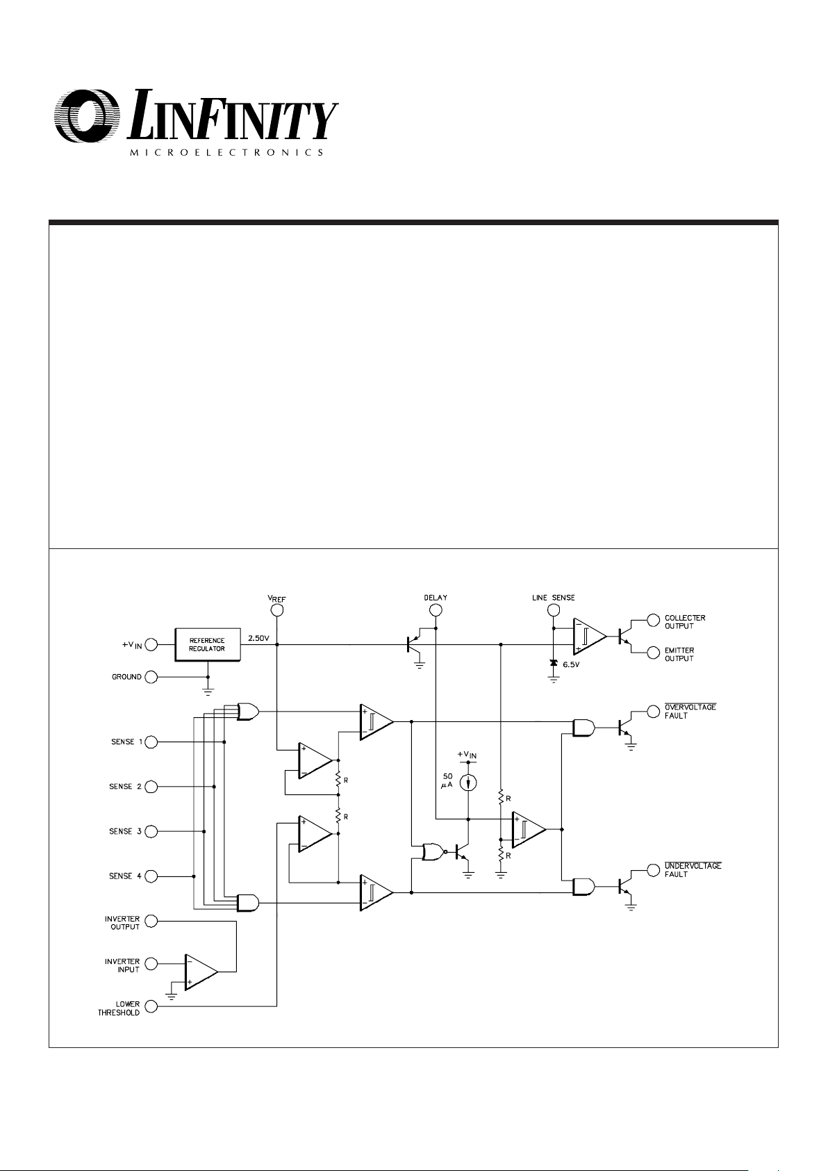
DESCRIPTION
The SG1548 is an integrated circuit capable of monitoring up to four
positive DC supply voltages simultaneously for overvoltage and
undervoltage fault conditions. An on-chip inverting op amp also
allows monitoring one negative DC voltage. The fault tolerance
window is accurately programmable from ±5% to ±40% using a simple
divider network on the 2.5V reference. A single external capacitor sets
the fault indication delay, eliminating false outputs due to switching
noise, logic transition current spikes, and short-term AC line interruptions. An additional comparator referenced to 2.5V allows the AC line
to be monitored for undervoltage conditions or for generation of a line
clock. The comparator can also be used for programmable
undervoltage lockout in a switching power supply. Uncommitted
collector and emitter outputs permit both inverting and non-inverting
operation. External availability of the precision 2.5V reference and
open-collector logic outputs permit expansion to monitor additional
voltage using available open-collector quad comparators.
FEATURES
••
••
• Monitors four DC voltages and the AC line
••
••
• Precision 2.5V ±1% low-drift reference
••
••
• Fault tolerance adjustable from ±5% to ±40%
••
••
• ±3% trip threshold tolerance over temperature
••
••
• Separate 10mA, 40V overvoltage, undervoltage
and AC line fault outputs
••
••
• Fault delay programmable with a single capacitor
••
••
• 30mV comparator hysteresis to prevent oscilla-
tions
••
••
• On-chip inverting op amp for negative voltage
••
••
• Open-collector output logic or expandability
••
••
• Operation from 4.5V to 40V supply
HIGH RELIABILITY FEATURES - SG1548
♦♦
♦♦
♦ Available to MIL-STD-883
♦♦
♦♦
♦ Radiation data available
♦♦
♦♦
♦ LMI level "S" processing available
BLOCK DIAGRAM
Page 2
11/91 Rev 1.2 5/97 LINFINITY Microelectronics Inc.
Copyright 1997 11861 Western Avenue
∞ ∞
∞ ∞
∞ Garden Grove, CA 92841
2 (714) 898-8121
∞∞
∞∞
∞ FAX: (714) 893-2570
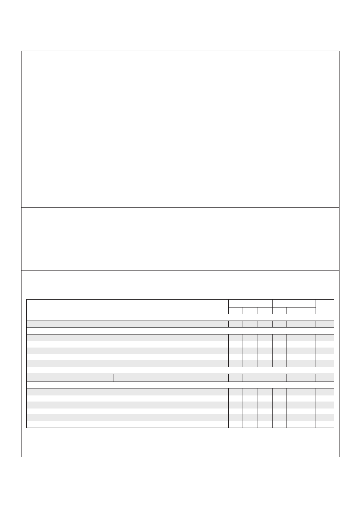
ABSOLUTE MAXIMUM RATINGS (Note 1)
SG1548/SG2548/SG3548
Inverting Op Amp Output Current ....................................
Operating Junction Temperature
Hermetic (J, L Packages) .............................................
Plastic (N, DW Packages) ............................................
Storage Temperature Range ............................
Lead Temperature ...........................................................
Supply Voltage (+VIN) ..........................................................
Fault Output Collector Voltage ............................................
Sense Input Voltage Range .................................
Fault Output Sink Current ................................................
Line Sense Input Current .................................................
Inverting Op Amp Input Current ........................................
40V
40V
-0.3V to 6.0V
20mA
±1mA
-5mA
25mA
150°C
150°C
-65°C to 150°C
300°C
Note 1. Values beyond which damage may occur.
THERMAL DATA
J Package:
Thermal Resistance-
Junction to Case, θ
JC
................... 30°C/W
Thermal Resistance-
Junction to Ambient, θ
JA
.............. 80°C/W
N Package:
Thermal Resistance-
Junction to Case, θ
JC
.................. 40°C/W
Thermal Resistance-
Junction to Ambient, θ
JA
............. 65°C/W
DW Package:
Thermal Resistance-
Junction to Case, θ
JC
.................. 40°C/W
Thermal Resistance-
Junction to Ambient, θ
JA
............. 95°C/W
L Package:
Thermal Resistance-
Junction to Case, θ
JC
.................. 35°C/W
Thermal Resistance-
Junction to Ambient, θ
JA
........... 120°C/W
Note A. Junction Temperature Calculation: TJ = TA + (PD x θJA).
Note B. The above numbers for
θJC are maximums for the limiting
thermal resistance of the package in a standard mounting configuration. The θ
JA
numbers are meant to be
guidelines for the thermal performance of the device/pcboard system. All of the above assume no ambient
airflow.
2.625
3.500
2.375
1.500
±0.6
100
DC Sense Inputs Section
V
PIN 1
= 0.95 x V
REF
V
PIN 1
= 0.60 x V
REF
V
PIN 1
= 0.95 x V
REF
V
PIN 1
= 0.60 x V
REF
V
SENSE
= 1.5V to 3.5V
+V
IN
= 4.5V to 35V
Overvoltage Threshold
Undervoltage Threshold
Input Bias Current
Threshold Supply Rejection
4.5V to 35V
5.0V to 35V
1.5V to 2.45V
±5% to ±40%
0 to 10mA
Supply Voltage Range
±25% Maximum Fault Window
(Note 3) ..............
±40% Maximum Fault Window ...........................
Lower Threshold Input Range .............................
Fault Tolerance Window Range ..........................
Fault Output Sink Current Range .............................
Line Sense Output Current Range ...........................
Voltage Reference Output Current ...........................
Operating Ambient Temperature Range
SG1548 .........................................................
SG2548 ...........................................................
SG3548 ...............................................................
0 to 10mA
0 to 10mA
-55°C to 125°C
-25°C to 85°C
0°C to 70°C
Note 2. Range over which the device is functional. Note 3. Limited by inverter amplifier positive swing at -55°C.
RECOMMENDED OPERATING CONDITIONS (Note 2)
ELECTRICAL CHARACTERISTICS
(Unless otherwise specified, these specifications apply over the operating ambient temperatures for SG1548 with -55°C ≤ TA ≤ 125°C, SG2548 with
-25°C ≤ TA ≤ 85°C, SG3548 with 0°C ≤ TA ≤ 70°C, and +VIN = 15V. Low duty cycle pulse testing techniques are used which maintains junction and case
temperatures equal to the ambient temperature.)
Reference Section (Note 4)
TJ = 25°C
Over Temperature
+V
IN
= 4.5V to 35V
I
L
= 0 to 10mA
V
REF
= 0V
Output Voltage
Line Regulation
Load Regulation
Short Circuit Current
4.8+VIN = 40VSupply Current mA10
Min. Typ. Max.
SG3548SG1548/2548
Test ConditionsParameter Units
Supply Section
-0.4V
PIN 1
= 1.5V to 2.45VInput Bias Current µA
Fault Window Generator Section
Min. Typ. Max.
10 4.8
2.475
2.450
10
2.500
1
3
25
2.525
2.550
5
10
50
2.475
2.450
10
2.500
1
3
25
2.525
2.550
5
10
50
V
V
mV
mV
mA
-2.0 -0.4 -2.0
2.547
3.396
2.304
1.455
60
2.704
3.606
2.447
1.545
±2.0
2.547
3.396
2.304
1.455
60
2.625
3.500
2.375
1.500
±0.6
100
2.704
3.606
2.447
1.545
±2.0
V
V
V
V
µA
dB
Note 4. IL = 0mA
Page 3

11/91 Rev 1.2 5/97 LINFINITY Microelectronics Inc.
Copyright 1997 11861 Western Avenue
∞ ∞
∞ ∞
∞ Garden Grove, CA 92841
3 (714) 898-8121
∞∞
∞∞
∞ FAX: (714) 893-2570
Fault Logic Outputs (Each output)
V
C
= 40V
I
C
= 10mA
Collector Leakage Current
Collector Saturation Voltage
2.500
25
1
1
0.2
13
AC Line Sense Section
V
PIN 5
= Low to High
V
PIN 5
= 2.5V
V
CE
= 40V
I
C
= 10mA
I
E
= 10mA
I
PIN 5
= 1mA
I
PIN 5
= -1mA
Comparator Threshold
Comparator Hysteresis
Input Bias Current
Collector Leakage Current
Collector Saturation Voltage
Emitter Output Voltage
Diode Clamp Voltage
2.440
12
6.0
-0.3
2.560
2
10
0.5
7.5
-1.0
2.440
12
6.0
-0.3
2.500
25
1
1
0.2
13
2
-0.3
3.5
1.0
100
15
100
3.2
72
5
72
Inverting Op Amp Section
(Note 5)
I
SOURCE
= 5mA
I
SINK
= 5mA
R
L
= 10K
+V
IN
= 4.5V to 35V
Input Offset Voltage
Input Bias Current
Output High Voltage
Output Low Voltage
Large Signal Voltage Gain
Output Source Current
Power Supply Rejection Ratio
mV
µA
V
V
dB
mA
dB
1.250
25
50
0.1
+3.2
1.200
32.5V
PIN 8
= 0V
I
PIN 8
= 0mA
I
PIN 8
= 0mA
Comparator Threshold
Comparator Hysteresis
Delay Charging Current
On Saturation Voltage
OFF Clamp Voltage
SG1548/SG2548/SG3548
Min. Typ. Max.
SG3548SG1548/2548
Test ConditionsParameter Units
ELECTRICAL CHARACTERISTICS (continued)
Min. Typ. Max.
APPLICATION INFORMATION
Note 5. +VIN = 4.5V.
Fault Delay Section
1.300
67.5
0.2
+3.6
1.200
32.5
1.250
25
50
0.1
+3.2
1.300
67.5
0.2
+3.6
V
mV
µA
V
V
15
-1.0
1.9
25
3.2
72
5
72
2
-0.3
3.5
1.0
100
15
100
15
-1.0
1.9
25
2.560
2
10
0.5
7.5
-1.0
V
mV
µA
µA
V
V
V
V
µA
V
10
0.5
1
0.2
10
0.5
1
0.2
SETTING THE FAULT TOLERANCE WINDOW
The fault tolerance window is set by applying a voltage less than
the +2.50Vreference to the Lower Threshold input (Pin 1). The
voltage is obtained by a resistor divider from the reference (Pin 3)
to ground. If ±5% tolerance is desired, then 95% of the reference
(+2.375V) is applied to Pin 1. If ±40% is wanted, then 60% of the
reference (+1.50V) is applied. In the example on the back page,
the tolerance is ±5%. The nominal overvoltage and undervoltage
thresholds are centered about the reference at +2.625V and
+2.375V (+2.500V ±0.125V).
SCALING THE MONITORED SUPPLY VOLTAGES
Each positive voltage to be monitored is divided down to +2.50V
with a resistor network and connected to one of the Sense inputs.
Unused Sense inputs should be connected to the reference. This
will not increase the bias current. A variation of the monitored
voltages out of the programmed tolerance range will cause the
appropriate overvoltage or undervoltage fault output to switch
LOW. The effective tolerance on any input may be broadened
with an additional resistor to the voltage reference. The example
on the back page shows a ±10% tolerance on the +5Vsupply
although the SG1548 is programmed for a ±5% tolerance. The
procedure for calculating the resistor value is found in the
SG1548 Application Note.
MONITORING A NEGATIVE VOLTAGE
A negative voltage can be converted to a positive one and
simultaneously scaled to +2.50V by using the internal operational
amplifier as an inverter. Only an input resistor and feedback
resistor are required.
SETTING THE FAULT DELAY
A single capacitor at the Delay pin sets the time an out-oftolerance fault must persist before a fault is actually declared.
This feature allows switching noise on the supplies to be rejected.
The delay time is given by: Delay = 25ms/µF .
AC LINE MONITORING
The AC line voltage can be monitored for single-cycle dropouts
with the few components shown in the example. A half-wave
rectifier charges the capacitor on positive line cycles. After the
positive peak and during the negative line cycle the capacitor
discharges from a fixed voltage controlled by the internal Zener
diode. If a positive cycle is missing, the capacitor discharges to
below the +2.5V trip point of the comparator, causing the output
transistor to turn on.
Page 4

11/91 Rev 1.2 5/97 LINFINITY Microelectronics Inc.
Copyright 1997 11861 Western Avenue
∞ ∞
∞ ∞
∞ Garden Grove, CA 92841
4 (714) 898-8121
∞∞
∞∞
∞ FAX: (714) 893-2570
SG1548/SG2548/SG3548
APPLICATION EXAMPLE
In this example, the SG1548 simultaneously monitors four DC voltages: +5V, +24V, and ±15V. Three different fault tolerances are
programmed: ±5% on the two 15V supplies, ±10% on the +5V supply, and ±20% on the +24V supply. The 5µF delay capacitor provides
125 milliseconds of fault delay.
CONNECTION DIAGRAMS & ORDERING INFORMATION (See Notes Below)
Ambient
Temperature Range
Part No.Package Connection Diagram
16-PIN CERAMIC DIP
J - PACKAGE
SG1548J/883B -55°C to 125°C
SG1548J -55°C to 125°C
SG2548J -25°C to 85°C
SG3548J 0°C to 70°C
SG2548N -25°C to 85°C
SG3548N 0°C to 70°C
16-PIN PLASTIC DIP
N - PACKAGE
2
3
4
5
6
7
8
11516
14
13
10
9
12
11
2
3
4
5
6
7
8
16-PIN WIDE BODY
PLASTIC S.O.I.C.
DW - PACKAGE
SG2548DW -25°C to 85°C
SG3548DW 0°C to 70°C
INV. OUTPUT
INV. INPUT
SENSE 4
SENSE 3
SENSE 2
SENSE 1
U.V. FAULT
O.V. FAULTDELAY
V
REF
GROUND
LOWER THRESHOLD
COLLECTOR OUTPUT
EMITTER OUTPUT
+V
IN
LINE SENSE
15
16
14
13
10
9
12
11
1
DELAY
V
REF
GROUND
LOWER THRESHOLD
+V
IN
LINE SENSE
COLLECTOR OUTPUT
EMITTER OUTPUT
INV. OUTPUT
INV. INPUT
SENSE 4
SENSE 3
SENSE 2
SENSE 1
U.V. FAULT
O.V. FAULT
20-PIN CERAMIC (LCC)
LEADLESS CHIP CARRIER
L- PACKAGE
SG1548L/883B -55°C to 125°C
SG1548L -55°C to 125° C
Note1. Contact factory for JAN and DESC product availability.
2. All parts are viewed from the top.
11. N.C.
12. O.V. FAULT
13. U.V. FAULT
14. SENSE 1
15. SENSE 2
16. N.C.
17. SENSE 3
18. SENSE 4
19. INV. INPUT
20. INV. OUTPUT
1. N.C.
2. LOWER THRESHOLD
3. GROUND
4. V
REF
5. +V
IN
6. N.C.
7. LINE SENSE
8. EMITTER OUTPUT
9. COLLECTOR
OUTPUT
4
5
6
7
8
321
9 11121310
14
15
16
17
18
20 19
10.DELAY
 Loading...