Datasheet SG1532T-883B, SG1532T-DESC, SG1532J, SG1532J-883B, SG1532J-DESC Datasheet (Microsemi Corporation)
...Page 1

SG1532/SG2532/SG3532
PRECISION GENERAL-PURPOSE REGULATOR
DESCRIPTION
This monolithic integrated circuit is a versatile, general-purpose voltage
regulator designed as a substantially improved replacement for the popular
SG723 device. The SG1532 series regulators retain all the versatility of the
SG723 but have the added benefits of operation with input voltages as low as
4.5 volts and as high as 50 volts; a low noise, low voltage reference;
temperature compensated, low threshold current limiting; and protective
circuits which include thermal shutdown and independent current limiting of
both the reference and output voltages. A separate remote shutdown terminal
is included . In the dual-in-line package an open collector output is available
for low input-output differential applications.
These devices are available in both hermetic 14-pin cerdip and 10-pin TO96 packages. In the T-package, these units are interchangeable with the LAS1000 and LAS-1100 regulators. The SG1532 is rated for operation over the
ambient temperature range of -55°C to 125°C while the SG2532 and SG3532
are intended for industrial applications of 0°C to 70°C.
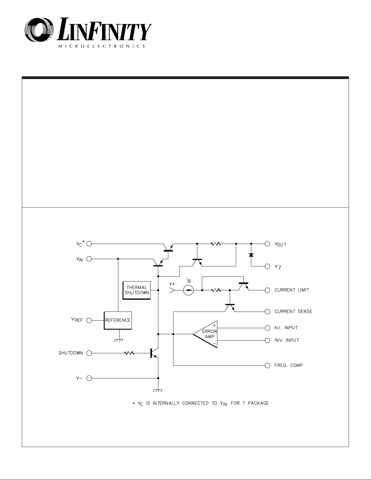
BLOCK DIAGRAM
FEATURES
••
• Input voltage range of 4.5V to 50V
••
••
• 2.5V low noise reference
••
••
• Independent shutdown terminal
••
••
• Improved line and load regulation
••
••
• 80mV current limit sense voltage
••
••
• Fully protected including thermal
••
shutdown
••
• Useful output current to 150mA
••
HIGH RELIABILITY FEATURES
-SG1532
♦♦
♦ Available to MIL-STD-883
♦♦
♦♦
♦ LMI level "S" processing available
♦♦
2/93 Rev 1.1 2/94 LINFINITY Microelectronics Inc.
Copyright 1994 11861 Western Avenue
1 (714) 898-8121
∞ ∞
∞ Garden Grove, CA 92841
∞ ∞
∞∞
∞ FAX: (714) 893-2570
∞∞
Page 2

ABSOLUTE MAXIMUM RATINGS (Note 1)
Pulse (50 ms) Input Voltage from VIN to V- .......................
Continuous Input Voltage from V
Input to Output Voltage Differential...................................
to V-............................
IN
Maximum Output Current ...........................................
Current from V
Note 1. Exceeding these ratings could cause damage to the device.
(J, L-Package only).............................
Z
50V
40V
40V
250mA
100mA
THERMAL DATA
SG1532/SG2532/SG3532
Current from V
Operating Junction Temperature
Hermetic (T, J, L-Packages).......................................
Storage Temperature Range ..........................
Lead Temperature (Soldering, 10 Seconds) .................
..........................................................
REF
-65°C to 150°C
25mA
150°C
300°C
J Package:
Thermal ResistanceThermal Resistance-
T Package:
Thermal ResistanceThermal Resistance-
L Package:
Thermal ResistanceThermal Resistance-
Junction to Case, θ
Junction to Ambient, θ
Junction to Case, θ
Junction to Ambient, θ
Junction to Case, θ
Junction to Ambient, θ
JC
JC
JC
.................. 30°C/W
.............. 80°C/W
JA
.................. 25°C/W
........... 130°C/W
JA
.................. 35°C/W
........... 120°C/W
JA
Note A. Junction Temperature Calculation: TJ = TA + (PD x θJA).
Note B. The above numbers for
θJC are maximums for the limiting
thermal resistance of the package in a standard mounting configuration. The θ
guidelines for the thermal performance of the device/pc-
numbers are meant to be
JA
board system. All of the above assume no ambient
airflow.
RECOMMENDED OPERATING CONDITIONS (Note 2)
Input Voltage Range
SG1532/SG2532 .................................................
SG3532 ..............................................................
Output Current Range .......................................
Note 2. Range over which the device is functional.
5V to 45V
5V to 36V
1mA to 100mA
Reference Current ........................................................
Zener Current (J & L-Packages only) ...........................
Operating Ambient Temperature Range
SG1532 ........................................................
SG2532/SG3532 ..............................................
-55°C to 125°C
0°C to 70°C
5mA
20mA
ELECTRICAL CHARACTERISTICS
(Unless otherwise specified, these specifications apply over the operating ambient temperatures for SG1532 with -55° C ≤ TA ≤ 125 °C, SG2532 with
0°C ≤ TA ≤ 70°C, SG3532 with 0°C ≤ TA ≤ 70°C, VIN = 10V, V
junction and case temperatures equal to the ambient temperature.)
Input Voltage Range
= 25°C
T
A
Output Voltage Range
Max Output Current
Min (V
Reference Voltage
Temperature Stability
IN
- V
OUT
)
(Note 4)
Ref Short Circuit Current
Line Regulation
(Note 3)
Load Regulation (Note 3)
Current Limit Sense Voltage
Shutdown Voltage Threshold
Shutdown Source Current
Zener Voltage
Standby Current
Error Amplifier Offset Voltage
R
= 0, V
SC
I
OUT
T
A
V
REF
8V ≤ V
8V ≤ V
1mA ≤ I
1mA ≤ I
R
SC
V
OUT
I
OUT
V
IN
OUT
= 100mA, TA = 25°C
= 25°C
= 0, TA = 25°C
≤ 40V
IN
≤ 20V, I
IN
≤ 25mA
OUT
≤ 100mA
OUT
= 100Ω, V
= high
= 10mA, (J and L-Packages only)
= 40V
Error Amplifier Input Bias
Current
= 5V, and I
OUT
Test ConditionsParameter
= 0, TA = 25°C
= 25mA
OUT
= 0V
OUT
= 1mA. Low duty cycle pulse testing techniques are used which maintains
OUT
SG1532/SG2532
SG3532
Min. Typ. Max. Min. Typ. Max.
4.5
4.7
2.0
2.40
2.35
0.06
0.40
100
6.0
2.50
0.005
0.005
0.01
0.002
0.002
0.08
0.70
175
1.7
15
200
6.4
2.5
2.0
4.0
50
50
38
250
2.0
2.60
2.65
0.015
25
0.01
0.02
0.004
0.005
0.10
1.0
300
7.2
3.5
10
15
4.5
4.7
2.0
2.40
2.35
0.06
0.40
100
6.0
175
1.7
2.50
0.005
15
0.005
0.01
0.002
0.002
0.08
0.70
200
6.4
2.5
2.0
4.0
40
40
38
250
2.0
2.60
2.65
0.015
25
0.02
0.03
0.004
0.005
0.10
1.0
300
7.2
3.5
15
20
Units
V
V
V
mA
V
V
V
%/°C
mA
%/V
%/V
%/mA
%/mA
V
V
µA
V
mA
mV
µA
2/93 Rev 1.1 2/94 LINFINITY Microelectronics Inc.
Copyright 1994 11861 Western Avenue
2 (714) 898-8121
∞ ∞
∞ Garden Grove, CA 92841
∞ ∞
∞∞
∞ FAX: (714) 893-2570
∞∞
Page 3

ELECTRICAL CHARACTERISTICS (continued)
SG1532/SG2532/SG3532
Test ConditionsParameter
Open Loop Gain
Ripple Rejection
Output Noise
(Note 4)
Long Term Stability (Note 4)
TA = 25°C
f = 120Hz, T
10Hz ≤ f ≤ 100KHz, T
= 30V, TA = 125°C
V
IN
= 25°C
A
= 25°C
A
Thermal Shutdown (Note 4)
Note 3. Applies for constant junction temperature. Temperature drift effects must be taken into account separately when the unit is operating under
conditions of high dissipation.
Note 4. These parameters, although guaranteed, are not tested in production.
SG1532/SG2532
Typ. Max.Min. Min.
66 68
66
50
0.3
1.0
175
SG3532
Typ. Max.
60 68
66
50
0.3
175
1.0
Units
dB
dB
µV
RMS
%/Khr
°C
CHARACTERISTIC CURVES
FIGURE 1.
STANDBY CURRENT
FIGURE 3.
CURRENT LIMITING
FIGURE 2.
MINIMUM INPUT-OUTPUT VOLTAGE
FIGURE 4.
RIPPLE REJECTION
2/93 Rev 1.1 2/94 LINFINITY Microelectronics Inc.
Copyright 1994 11861 Western Avenue
3 (714) 898-8121
∞ ∞
∞ Garden Grove, CA 92841
∞ ∞
∞∞
∞ FAX: (714) 893-2570
∞∞
Page 4

CHARACTERISTIC CURVES (continued)
SG1532/SG2532/SG3532
FIGURE 5.
FREQUENCY RESPONSE
APPLICATION INFORMATION
FIGURE 7 - 90% EFFICIENT LINEAR REGULATOR
Output Voltage = 5V Max Output Current = 3A
Min (VIN-V
Load Reg 0-2A = 20mV
Notes:
) at 2A = 0.4V Line Reg 6-30V = 10 mV
OUT
FIGURE 6.
TRANSIENT RESPONSE
FIGURE 8 - HIGH CURRENT REGULATOR WITH FOLDBACK
CURRENT LIMITING AND REMOTE SHUTDOWN
Output Voltage = 5V Line Reg 10-30V = 3mV
Max Output Current = 8A Load Reg 0-5A = 17mV
at No Load = 6.9V Short Circuit Current = 1.8A
Min V
IN
Min VIN at 5A = 8.2V
Note:
For output voltages above 8V and load currents
which allow PNP base current to be limited to
* 100Ω surge limiting resistor should be used for
output voltages above 8V.
25mA, the internal zener may be used, eliminating the need for the two external diodes and the
divider on V
REF
.
RSC can be eliminated if the 200mA current limit on
V
is adequate. Overall current limiting is
OUT
dependent upon PNP Beta. For greater accuracy, load currrent may be sensed in the ground
line.
2/93 Rev 1.1 2/94 LINFINITY Microelectronics Inc.
Copyright 1994 11861 Western Avenue
4 (714) 898-8121
∞ ∞
∞ Garden Grove, CA 92841
∞ ∞
∞∞
∞ FAX: (714) 893-2570
∞∞
Page 5

APPLICATION INFORMATION
SG1532/SG2532/SG3532
FIGURE 9 - HIGH EFFICIENCY LOW VOLTAGE REGULATOR
Output Voltage = 5V Line Reg 7-20V = 10mV
Max Output Current = 9A Load Reg 0-5A = 25mV
at 5A = 7.0V Constant Current Limiting
Min V
IN
FIGURE 10 - BASIC LOW CURRENT REGULATOR
V
OUT
C
C
I
OUT
CONNECTION DIAGRAMS & ORDERING INFORMATION (See Notes Below)
Ambient
Temperature Range
Connection Diagram
NON-INVERTING INPUT
(Notes 3 & 4)
INVERTING INPUT
14-PIN CERAMIC DIP
J - PACKAGE
10-PIN METAL CAN
T - PACKAGE
Part No.Package
SG1532J/883B -55°C to 125°C
SG1532J/DESC -55°C to 125°C
SG1532J -55°C to 125°C
SG2532J 0°C to 70°C
SG3532J 0°C to 70°C
SG1532T/883B -55°C to 125°C
SG1532T/DESC -55°C to 125°C
SG1532T -55°C to 125°C
SG2532T 0°C to 70°C
SG3532T 0°C to 70°C
R
REF
1+
R
1
2
= V
= 1000 pF
≤ 100mA
CURRENT LIMIT
CURRENT SENSE
INVERTING INPUT
NON-INVERTING
INPUT
ISC=
R
3
1
N.C.
2
3
4
5
6
V
REF
7
V-
CURRENT LIMIT
1
2
3
4
V
REF
Sense Voltage
R
SC
R1 R
2
=
R1+R
2
14
N.C.
13
FREQ. COMPENSATION
12
V
IN
11
V
C
10
V
OUT
9
V
Z
8
SHUTDOWN
10
9
8
7
6
5
V
OUT
V-
FREQ. COMPENSATIONCURRENT SENSE
& V
V
IN
C
SHUTDOWN
20-PIN CERAMIC
LEADLESS CHIP CARRIER
L- PACKAGE
Note 1. Contact factory for JAN and DESC product availablity.
2. All packages are viewed from the top.
2/93 Rev 1.1 2/94 LINFINITY Microelectronics Inc.
Copyright 1994 11861 Western Avenue
SG1532L/883B -55° C to 125°C
SG1532L -55°C to 125°C
5 (714) 898-8121
2. CURRENT LIMIT
3. CURRENT SENSE
4. N.C.
5. INVERTING INPUT
6. N.C.
7. N. I. INPUT
8. V
REF
9. N.C.
10. V-
Note 3. V
output is not available in T-package.
Z
4. Pin 5 is connected to case.
4
5
6
7
8
32120191. N.C.
9
10 11 12 13
11. N.C.
12. SHUTDOWN
13. V
18
Z
14. N.C.
17
15. V
OUT
16
16. N.C.
15
17. V
C
14
18. V
IN
19. N.C.
20. FREQ. COMP.
∞ ∞
∞ Garden Grove, CA 92841
∞ ∞
∞∞
∞ FAX: (714) 893-2570
∞∞
 Loading...