

Datasheet SG1731J, SG1731J-883B, SG2731J, SG2731N, SG3731J Datasheet (Microsemi Corporation)
...Page 1
SG1731/SG2731/SG3731
DC MOTOR PULSE WIDTH MODULATOR
DESCRIPTION
The SG1731 is a pulse width modulator circuit designed specifically for DC motor
control. It provides a bi-directional pulse train output in response to the magnitude
and polarity of an analog error signal input. The device is useful as the control
element in motor-driven servo systems for precision positioning and speed control,
as well as in audio modulators and amplifiers using carrier frequencies to 350 KHz.
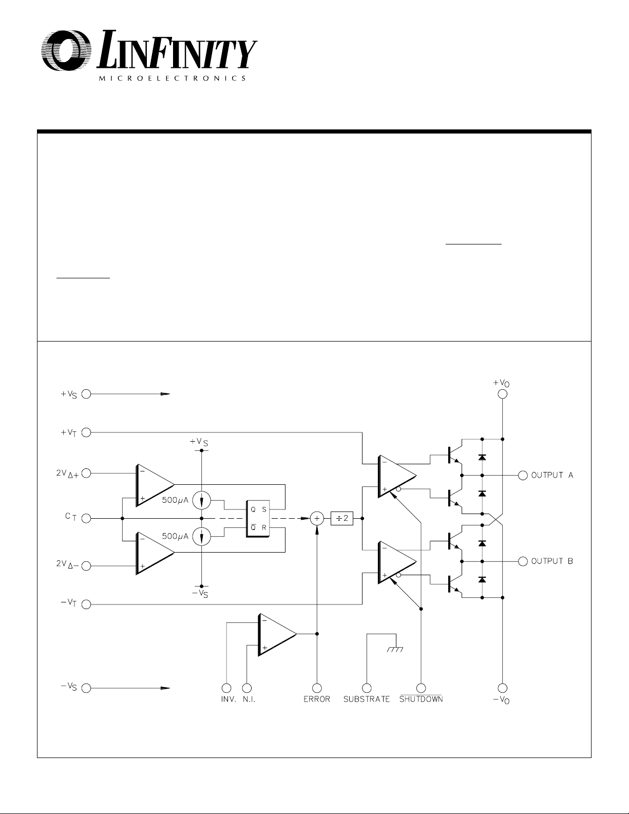
The circuit contains a triangle waveform oscillator, a wideband operational amplifier
for error voltage generation, a summing/scaling network for level-shifting the
triangle waveform, externally programmable PWM comparators and dual ±100mA,
±22V totem pole drivers with commutation diodes for full bridge output. A
SHUTDOWN terminal forces the drivers into a floating high-impedance state when
driven LOW. Supply voltage to the control circuitry and to the output drivers may be
from either dual positive and negative supplies, or single-ended.
BLOCK DIAGRAM
FEATURES
••
±±
•
±3.5V to
••
±±
••
±±
•
±2.5V to
••
±±
••
• Dual 100mA source/sink output
••
drivers
••
• 5KHz to 350KHz oscillator range
••
••
• High slew rate error amplifier
••
••
• Adjustable deadband operation
••
••
• Digital SHUTDOWN input
••
±±
±15V control supply
±±
±±
±22V driver supply
±±
HIGH RELIABILITY FEATURES
- SG1731
♦♦
♦ Available to MIL-STD-883
♦♦
♦♦
♦ LMI level “S” processing available
♦♦
4/90 Rev 1.3 9/99 LINFINITY Microelectronics Inc.
Copyright 1999 11861 Western Avenue
1 (714) 898-8121
∞ ∞
∞ Garden Grove, CA 92841
∞ ∞
∞∞
∞ FAX: (714) 893-2570
∞∞
Page 2
ABSOLUTE MAXIMUM RATINGS (Note1)
Supply Voltage (±VS) ........................................................ ±18V
Analog Inputs....................................................................... ±V
Digital Inputs (SHUTDOWN) .................... -VS-0.3V to -VS+18V
Output Driver Supply Voltage (±V
Source/Sink Output Current (continuous) .................... 200mA
) ................................. ±25V
O
Source/Sink Output Current (peak, 500ns).................. 400mA
Note 1. Values beyond which damage may occur.
THERMAL DATA
SG1731/SG2731/SG3731
Output Driver Diode Current (continuous) .................... 200mA
Output Driver Diode Current (peak, 500ns) .................. 400mA
S
Operating Junction Temperature
Hermetic (J - Package) ............................................... 150°C
Plastic (N - Package) .................................................. 150 °C
Storage Temperature Range ............................ -65°C to 150°C
Lead Temperature (Soldering, 10 Seconds) .................. 300 °C
J Package:
Thermal Resistance-Junction to Case, θ
Thermal Resistance-Junction to Ambient, θJA.......... 80°C/W
.............. 30°C/W
JC
N Package:
Thermal Resistance-Junction to Case, θ
Thermal Resistance-Junction to Ambient, θJA......... 65°C/W
.............. 40°C/W
JC
Note A. Junction Temperature Calculation: TJ = TA + (PD x θJA).
Note B. The above numbers for θ
resistance of the package in a standard mounting configuration.
The θJA numbers are meant to be guidelines for the thermal
performance of the device/pc-board system. All of the above
assume no ambient airflow.
are maximums for the limiting thermal
JC
RECOMMENDED OPERATING CONDITIONS (Note 2)
Supply Voltage Range (±VS)............................... ±3.5V to ±15V
Error Amp Common-Mode Range ............... -VS + 3V to VS - 3V
Output Driver Supply Voltage Range.................. ±2.5V to ±22V
Source/Sink Output Current (continuous) .................... 100mA
Source/Sink Output Current (peak, 500ns) .................. 200mA
Output Driver Diode Current (continuous) .................... 100mA
Output Driver Diode Current (peak, 500ns) .................. 200mA
Note 2. Range over which the device is functional and parameter limits are guaranteed.
Oscillator Frequency Range ........................... 10Hz to 350KHz
Oscillator Voltage (Peak-to-Peak) .............................1V to 10V
Oscillator Timing Capacitor (CT) ....................... 200pF to 2.5µF
Operating Ambient Temperature Range
SG1731 ........................................................ -55°C to 125°C
SG2731 ........................................................... -25°C to 85°C
SG3731 .............................................................. 0°C to 70°C
ELECTRICAL CHARACTERISTICS
(Unless otherwise specified, these specfiications apply over the operating ambient temperatures for SG1731 with -55°C ≤ TA ≤ 125°C, SG2731 with
-25°C ≤ TA ≤ 85°C, SG3731 with 0°C ≤ TA ≤ 70°C, VS = ±15V, and VO = ±22V. Low duty cycle pulse testing techniques are used which maintains junction
and case temperatures equal to the ambient temperature.)
Parameter Units
Oscillator Section
CT Charging Current
2V∆± Input Bias Current
Initial Oscillator Frequency
Temperature Stability
(Note 3)
TA = 25°C
TA = T
MIN
VCM = ±5V
CT = 1000pF, 2V∆± = ±5V,TA = 25°C
CT = 1000pF, 2V∆± = ±5V
Error Amplifier Section (Note 5)
Input Offset Voltage
Input Bias Current
Input Offset Current
Open Loop Voltage Gain
Output Voltage Swing
RL = 2KΩ
RL = 2KΩ
Common-Mode Rejection Ratio
Slew Rate (Notes 3 and 4)
Unity Gain Bandwidth (Notes 3 and 4)
TA = 25°C
TA = 25°C
PWM Comparators
Input Bias Current 6 µA±VT = ±3V
Test Conditions
to T
MAX
SG1731/2731/3731
Min. Typ. Max.
500
450
400
550
600
-20
25.0
22.5
27.5
10
10
3
600
70
±10
70
5
10
0.7
1
µA
µA
µA
KHz
%
mV
µA
nA
dB
V
dB
V/µs
MHz
4/90 Rev 1.3 9/99 LINFINITY Microelectronics Inc.
Copyright 1999 11861 Western Avenue
2 (714) 898-8121
∞ ∞
∞ Garden Grove, CA 92841
∞ ∞
∞∞
∞ FAX: (714) 893-2570
∞∞
Page 3

ELECTRICAL CHARACTERISTICS (continued)
SG1731/SG2731/SG3731
Parameter
SHUTDOWN Section
Logic Threshold
SHUTDOWN HIGH Current
SHUTDOWN LOW Current
= -3.5V to -15V
-V
S
V
SHUTDOWN
V
SHUTDOWN
= -VS+2.4V
= -V
S
Output Drivers (Each Output)
HIGH Output Voltage
LOW Output Voltage
Driver Risetime
Driver Falltime
= 20mA
I
SOURCE
= 100mA
I
SOURCE
I
= 20mA
SINK
I
= 100mA
SINK
CL = 1000pF
CL = 1000pF
Total Supply Current
VS Supply Current
VO Supply Current
Note 3. These parameters, although guaranteed, are not tested in production.
Note 4. Unity Gain Inverting 10KΩ Feedback Resistance.
V
SHUTDOWN
V
SHUTDOWN
= -VS + 0.8V
= -VS + 0.8V
APPLICATION INFORMATION
SUPPLY VOLTAGE
The SG1731 requires a supply voltage for the control circuitry (V
and for the power output drivers (V
). Each supply may be either
O
balanced positive and negative with respect to ground, or singleended. The only restrictions are:
1.The voltage between +V
and -VS must be at least 7.0V; but
S
no more than 44V.
2.The voltage between +VO and -VO must be at least 5.0V; but
no more than 44V.
must be at least 5V more positive than -VS. This
3.+V
O
eliminates the combination of a single-ended positive control
supply with a single-ended negative driver supply.
)
S
Test Conditions Units
Note 5. VCM = ±12V.
SG1731/2731/3731
Min. Typ. Max.
VS+0.8
VS+2.0
400
-1.0
19.2
19.0
-19.2
-19.0
300
300
14
6
V
µA
mA
V
V
V
V
ns
ns
mA
mA
As a design aid, the solutions to Equation 1 over the
recommended range of T
Figure 1. The lower limit on T
maximum frequency of 350 KHz. The maximum value of V
(2V
∆+) - (2V∆-), is 10V peak-to-peak for linear waveforms.
OSC
and V
are given in graphic form in
OSC
is 1.85µs, corresponding to a
OSC
OSC
,
SUBSTRATE CONNECTION
The substrate connection (Pin 10) must always be connected to
either -V
or -VO, whichever is more negative. The substrate must
S
also be well bypassed to ground with a high quality capacitor.
OSCILLATOR
FIGURE 1 - SG1731 OSCILLATOR PERIOD VS. V
OSC
AND C
T
ERROR AMPLIFIER
The triangle oscillator consists of two voltage comparators, a set/
reset flip-flop, a bi-directional 500µA current source, and an
external timing capacitor C
. A positive reference voltage (2V∆+)
T
applied to Pin 2 determines the positive peak value of the triangle,
and a negative reference voltage (2V∆-) at Pin 7 sets the negative
peak value of the triangle waveform.
Since the value of the internal current source is fixed at a nominal
±500µA, the oscillator period is a function of the selected peakto-peak voltage excursion and the value of C
. The theoretical
T
expression for the oscillator period is:
2CT dV
= (Eq.1)
T
OSC
where CT is the timing capacitor in Farads and dV is V
5 x 10
-4
in Volts
OSC
peak-to-peak.
4/90 Rev 1.3 9/99 LINFINITY Microelectronics Inc.
Copyright 1999 11861 Western Avenue
The error amplifier of the SG1731 is a conventional internallycompensated operational amplifier with low output impedance.
All of the usual feedback and frequency compensation
techniques may be use to control the closed-loop gain
characteristics. The control supply voltage ±V
input common mode range and output voltage swing; both will
will determine the
S
extend to within 3V of the VS supply.
PULSE WIDTH MODULATION
Pulse width modulation occurs by comparing the triangle
waveform to a fixed upper (+V
) and lower (-VT) threshold
T
voltage. A crossing above the upper threshold causes
Output A to switch to the HIGH state, and a crossing below
∞ ∞
∞ Garden Grove, CA 92841
∞ ∞
3 (714) 898-8121
∞∞
∞ FAX: (714) 893-2570
∞∞
Page 4

APPLICATION INFORMATION (continued)
the lower threshold causes Output B to switch to the HIGH state.
If ±V
is less than ±8V then ±VT can be obtained with resistors from
S
. If ±VS is greater than ±8V use zeners.
±V
S
Threshold crossings are generated by shifting the triangle
waveform up and down with the error voltage (Pin 5). A positive
error voltage will result in a pulse width modulated output at
Driver A (Pin 13). Similarly, a negative error voltage produces a
pulse train at Driver B (Pin 12). Figure 2 illustrates this process
for the case where V
∆+ is greater than V
It is important to note that the triangle shifting circuit also
attenuates the waveform seen at C
in a waveform at the PWM comparators with a positive peak of
V∆+ and a negative peak of V
when selecting the values for +V
∆-, and must be taken into account
and -VT.
T
.
T
by a factor of 2. This results
T
SG1731/SG2731/SG3731
APPLICATION CIRCUITS
FIGURE 2 - PULSE WIDTH MODULATION WITH NO DEADBAND
FIGURE 3
In this simple battery-powered position servo, the control supply
and driver supply are both single-ended positive with respect to
A high torque position servo is obtained by buffering the output
drivers to obtain higher output current.
FIGURE 4
ground.
4/90 Rev 1.3 9/99 LINFINITY Microelectronics Inc.
Copyright 1999 11861 Western Avenue
4 (714) 898-8121
∞ ∞
∞ Garden Grove, CA 92841
∞ ∞
∞∞
∞ FAX: (714) 893-2570
∞∞
Page 5

APPLICATION CIRCUITS
SG1731/SG2731/SG3731
FIGURE 5
Bi-directional speed control results when the feedback voltage
transducer is a tachometer.
The two-quadrant transfer function of the SG1731 is ideal for
pulse width modulated audio power amplifiers.
CONNECTION DIAGRAMS & ORDERING INFORMATION (See Note Below)
Ambient
Temperature Range
Connection Diagram
16-PIN CERAMIC DIP
J - PACKAGE
16-PIN PLASTIC DIP
N - PACKAGE
Part No.Package
SG1731J/883B -55°C to 125°C
SG1731J -55°C to 125°C
SG2731J -25°C to 85°C
SG3731J 0°C to 65°C
SG2731N -25°C to 85°C
SG3731N 0°C to 65°C
FIGURE 6
1916
+V
T
2
2V∆+ SHUTDOWN
N. I. INPUT +V
INV. INPUT
ERROR
C
T
2V∆-
-V
T
15
14
3
4
13
5
12
11
6
10
7
8
+V
S
O
OUTPUT A
OUTPUT B
-V
O
SUBSTRATE
-V
S
Note 1. All packages are viewed from the top.
Note 2. Contact factory for flatpack and leadless chip carrier availability.
4/90 Rev 1.3 9/99 LINFINITY Microelectronics Inc.
Copyright 1999 11861 Western Avenue
5 (714) 898-8121
∞ ∞
∞ Garden Grove, CA 92841
∞ ∞
∞∞
∞ FAX: (714) 893-2570
∞∞
 Loading...