

Datasheet SG1644J, SG1644J-883B, SG1644J-DESC, SG1644L-883B, SG1644L-DESC Datasheet (Microsemi Corporation)
...Page 1
SG1644/SG2644/SG3644
DUAL HIGH SPEED DRIVER
DESCRIPTION
The SG1644, 2644, 3644 is a dual non-inverting monolithic high
speed driver. This device utilizes high voltage Schottky logic to
convert TTL signals to high speed outputs up to 18V. The totem
pole outputs have 3A peak current capability, which enables them
to drive 1000pF loads in typically less than 25ns. These speeds
make it ideal for driving power MOSFETs and other large capacitive loads requiring high speed switching.
In addition to the standard packages, Silicon General offers the 16
pin S.O.I.C. (DW-package) for commercial and industrial applications, and the Hermetic TO-66 (R-package) for military use.
These packages offer improved thermal performance for applications requiring high frequencies and/or high peak currents.
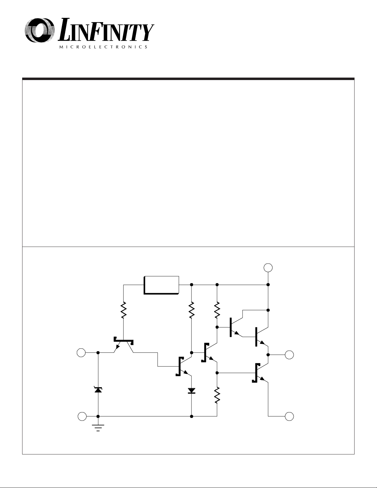
EQUIVALENT CIRCUIT SCHEMATIC
FEATURES
••
• Totem pole outputs with 3.0A peak current
••
capability.
••
• Supply voltage to 22V.
••
••
• Rise and fall times less than 25ns.
••
••
• Propagation delays less than 20ns.
••
••
• Non-inverting high-speed high-voltage Schottky
••
logic.
••
• Efficient operation at high frequency.
••
••
• Available in:
••
8 Pin Plastic and Ceramic DIP
14 Pin Ceramic DIP
16 Pin Plastic S.O.I.C.
20 Pin LCC
TO-99
TO-66
HIGH RELIABILITY FEATURES - SG1644
♦♦
♦ Available to MIL-STD-883
♦♦
♦♦
♦ Radiation data available
♦♦
♦♦
♦ LMI level "S" processing available
♦♦
V
CC
INV. INPUT
LOGIC
GND
(Substrate)
2.5K
6.5V
V
REG
3K3K
OUTPUT
POWER
GND
9/91 Rev 1.2 6/97 LINFINITY Microelectronics Inc.
Copyright 1997 11861 Western Avenue
1 (714) 898-8121
∞ ∞
∞ Garden Grove, CA 92841
∞ ∞
∞∞
∞ FAX: (714) 893-2570
∞∞
Page 2
ABSOLUTE MAXIMUM RATINGS (Note 1)
SG1644/SG2644/SG3644
Supply Voltage (VCC) ...........................................................
Logic Input Voltage ...............................................................
Source/Sink Output Current (Each Output)
Continuous ...................................................................
Pulse, 500ns ................................................................
Note 1. Exceeding these ratings could cause damage to the device. All voltages are with respect to ground. All currents are positive into the
specified terminal.
22V
7V
±0.5A
±3.0A
Operating Junction Temperature
Hermetic (J, T, Y, R-Packages) ....................................
Plastic (M, DW, L-Packages) ......................................
Storage Temperature Range ............................
-65°C to 150°C
Lead Temperature (Soldering, 10 Seconds) ..................
THERMAL DATA
J Package:
Thermal ResistanceThermal Resistance-
Y Package:
Thermal ResistanceThermal Resistance-
M Package:
Thermal ResistanceThermal Resistance-
DW Package:
Thermal ResistanceThermal Resistance-
T Package:
Thermal ResistanceThermal Resistance-
Junction to Case, θ
Junction to Ambient, θ
Junction to Case, θ
Junction to Ambient, θ
Junction to Case, θ
Junction to Ambient, θ
Junction to Case, θ
Junction to Ambient, θ
Junction to Case, θ
Junction to Ambient, θ
JC
JC
JC
JC
JC
.................. 30°C/W
............... 80°C/W
JA
.................. 50°C/W
............. 130°C/W
JA
.................. 60°C/W
.............. 95°C/W
JA
.................. 40°C/W
............... 95°C/W
JA
.................. 25°C/W
............ 130°C/W
JA
R Package:
Thermal ResistanceThermal Resistance-
Junction to Case, θ
Junction to Ambient, θ
L Package:
Thermal ResistanceThermal Resistance-
Note A. Junction Temperature Calculation: TJ = TA + (PD x θJA).
Note B. The above numbers for θ
resistance of the package in a standard mounting configuration.
numbers are meant to be guidelines for the thermal
The θ
JA
performance of the device/pc-board system. All of the above
assume no ambient airflow.
Junction to Case, θ
Junction to Ambient, θ
are maximums for the limiting thermal
JC
................. 5.0°C/W
JC
.............. 40°C/W
JA
.................. 35°C/W
JC
............ 120°C/W
JA
RECOMMENDED OPERATING CONDITIONS (Note 2)
Supply Voltage (V
Frequency Range ...............................................
) ..................................
CC
4.5V to 20V (Note 3)
DC to 1.5MHz
Peak Pulse Current ............................................................
Logic Input Voltage .................................................
Note 2. Range over which the device is functional.
Note 3. AC performance has been optimized for V
-0.5 to 5.5V
= 8V to 20V.
CC
±3A
Operating Ambient Temperature Range (T
SG1644 .........................................................
)
A
SG2644 ...........................................................
SG3644 ...............................................................
-55°C to 125°C
-25°C to 85°C
0°C to 70°C
150°C
150°C
300°C
ELECTRICAL CHARACTERISTICS
(Unless otherwise specified, these specfiications apply over the operating ambient temperatures for SG1644 with -55°C ≤ TA ≤ 125°C, SG2644 with -25°C
≤ TA ≤ 85°C, SG3644 with 0°C ≤ TA ≤ 70°C, and VCC = 20V. Low duty cycle pulse testing techniques are used which maintains junction and case
temperatures equal to the ambient temperature.)
Test ConditionsParameter
Static Characteristics
Logic 1 Input Voltage
Logic 0 Input Voltage
Input High Current
Input High Current
Input Low Current
Input Clamp Voltage
Output High Voltage
(Note 4)
Output Low Voltage (Note 4)
Supply Current Outputs Low
Supply Current Outputs High
Note 4. VCC = 10V to 20V.
9/91 Rev 1.2 6/97 LINFINITY Microelectronics Inc.
Copyright 1997 11861 Western Avenue
VIN = 2.4V
= 5.5V
V
IN
V
= 0V
IN
= -10mA
I
IN
I
= -200mA
OUT
I
= 200mA
OUT
= 0V (both inputs)
V
IN
V
= 2.4V (both inputs)
IN
2 (714) 898-8121
SG1644/2644/3644
Min. Typ. Max.
2.0
0.7
500
1.0
-4
-1.5
V
-3
CC
1.0
18
27
7.5
12
∞ ∞
∞ Garden Grove, CA 92841
∞ ∞
∞∞
∞ FAX: (714) 893-2570
∞∞
Units
V
V
µA
mA
mA
V
V
V
mA
mA
Page 3
ELECTRICAL CHARACTERISTICS (continued)
SG1644/SG2644/SG3644
Test Conditions (Figure 1)Parameter
SG1644/2644/3644
TA= 25
°°
°C
°°
Min. Typ. Max.
Dynamic Characteristics
Propagation Delay High-Low
(TPHL)
Propagation Delay Low-High
(TPLH)
Rise Time (TTLH)
Fall Time (TTHL)
Supply Current (I
(both outputs)
Note 5. These parameters, specified at 1000pF, although guaranteed over recommended operating conditions, are not tested in production.
Note 6. VCC = 15V.
)
CC
(Note 6)
CL = 1000pF (Note 5)
CL = 2500pF
= 1000pF (Note 5)
C
L
CL = 2500pF
= 1000pF (Note 5)
C
L
CL = 2500pF
C
= 1000pF (Note 5)
L
CL = 2500pF
C
= 2500pF, Freq. = 200KHz
L
Duty Cycle = 50%
26
18
30
30
30
30
35
25
30
30
40
25
40
35
SG1644
TA=-55
°°
°C to 125
°°
°°
°C
°°
Min. Typ. Max.
40
50
30
40
35
50
30
50
40
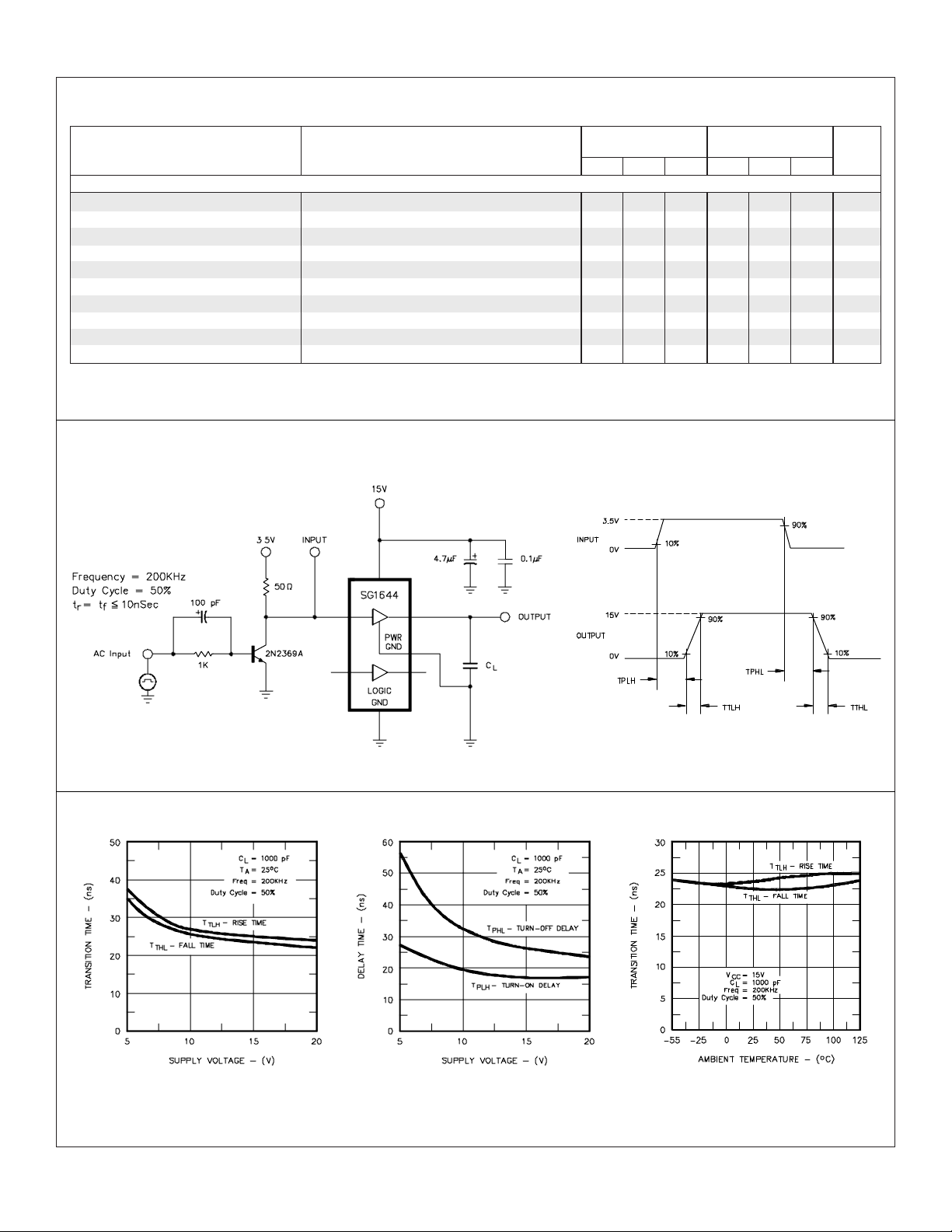
AC TEST CIRCUIT AND SWITCHING TIME WAVEFORMS - FIGURE 1
Units
ns
ns
ns
ns
ns
ns
ns
ns
mA
CHARACTERISTIC CURVES
FIGURE 2.
TRANSITION TIMES VS. SUPPLY VOLTAGE
9/91 Rev 1.2 6/97 LINFINITY Microelectronics Inc.
Copyright 1997 11861 Western Avenue
FIGURE 3.
PROPAGATION DELAY VS. SUPPLY VOLTAGE
3 (714) 898-8121
FIGURE 4.
TRANSITION TIMES VS. AMBIENT TEMPERATURE
∞ ∞
∞ Garden Grove, CA 92841
∞ ∞
∞∞
∞ FAX: (714) 893-2570
∞∞
Page 4

CHARACTERISTIC CURVES (continued)
SG1644/SG2644/SG3644
FIGURE 5.
PROPAGATION DELAY VS. AMBIENT TEMPERATURE
FIGURE 8.
HIGH SIDE SATURATION VS. OUTPUT CURRENT
FIGURE 6.
TRANSITION TIMES VS. CAPACITIVE LOAD
FIGURE 9.
LOW SIDE SATURATION VS. OUTPUT CURRENT
FIGURE 7.
SUPPLY CURRENT VS. CAPACITANCE LOAD
FIGURE 10.
SUPPLY CURRENT VS. FREQUENCY
FIGURE 11.
SUPPLY CURRENT VS. FREQUENCY
9/91 Rev 1.2 6/97 LINFINITY Microelectronics Inc.
Copyright 1997 11861 Western Avenue
4 (714) 898-8121
∞ ∞
∞ Garden Grove, CA 92841
∞ ∞
∞∞
∞ FAX: (714) 893-2570
∞∞
Page 5

APPLICATION INFORMATION
SG1644/SG2644/SG3644
POWER DISSIPATION
The SG1644, while more energy-efficient than earlier gold-doped
driver IC’s, can still dissipate considerable power because of its
high peak current capability at high frequencies. Total power
dissipation in any specific application will be the sum of the DC or
steady-state power dissipation, and the AC dissipation caused by
driving capacitive loads.
The DC power dissipation is given by:
= +VCC · ICC [1]
P
DC
where I
dependent.
is a function of the driver state, and hence is duty-cycle
CC
The AC power dissipation is proportional to the switching frequency, the load capacitance, and the square of the output
voltage. In most applications, the driver is constantly changing
state, and the AC contribution becomes dominant when the
frequency exceeds 100-200KHz.
The SG1644 driver family is available in a variety of packages to
accommodate a wide range of operating temperatures and power
dissipation requirements. The Absolute Maximums section of the
data sheet includes two graphs to aid the designer in choosing an
appropriate package for his design.
The designer should first determine the actual power dissipation
of the driver by referring to the curves in the data sheet relating
operating current to supply voltage, switching frequency, and
capacitive load. These curves were generated from data taken on
actual devices. The designer can then refer to the Absolute
Maximum Thermal Dissipation curves to choose a package type,
and to determine if heat-sinking is required.
DESIGN EXAMPLE
Given: Two 2500pF loads must be driven push-pull from a +15 volt
supply at 100KHz. The application is a commercial one in which
the maximum ambient temperature is +50°C, and cost is important.
1. From Figure 11, the average driver current consumption
under these conditions will be 18mA, and the power dissipation
will be 15volts x 18mA, or 270mW.
2. From the ambient thermal characteristic curve, it can be seen
that the M package, which is an 8-pin plastic DIP with a copper
lead frame, has more than enough thermal conductance from
junction to ambient to support operation at an ambient temperature of +50°C. The SG36446M driver would be specified for this
application.
SUPPLY BYPASSING
Since the SG1644 can deliver peak currents above 3amps under
some load conditions, adequate supply bypassing is essential for
proper operation. Two capacitors in parallel are recommended to
guarantee low supply impedance over a wide bandwidth: a 0.1µF
ceramic disk capacitor for high frequencies, and a 4.7µF solid
tantalum capacitor for energy storage. In military applications, a
CK05 or CK06 ceramic operator with a CSR-13 tantalum capacitor is an effective combination. For commercial applications, any
low-inductance ceramic disk capacitor teamed with a Sprague
150D or equivalent low ESR capacitor will work well. The
capacitors must be located as close as physically possible to the
VCC pin, with combined lead and pc board trace lengths held to
less than 0.5 inches.
GROUNDING CONSIDERATIONS
The ability of the SG1644 to deliver high peak currents into
capacitive loads can cause undesirable negative transients on
the logic and power grounds. To avoid this, a low inductance
ground path should be considered for each output to return the
high peak currents back to it’s own ground point. A ground plane
is recommended for best performance. If space for a ground
plane is not available, make the paths as short and as wide as
possible. The logic ground can be returned to the supply bypass
capacitor and be connected at one point to the power grounds.
LOGIC INTERFACE
The logic input of the 1644 is designed to accept standard DCcoupled 5 volt logic swings, with no speed-up capacitors required.
If the input signal voltage exceeds 6 volts, the input pin must be
protected against the excessive voltage in the HIGH state. Either
a high speed blocking diode must be used, or a resistive divider
to attenuate the logic swing is necessary.
LAYOUT FOR HIGH SPEED
The SG1644 can generate relatively large voltage excursions
with rise and fall times around 20-30 nanoseconds with light
capacitive loads. A Fourier analysis of these time domain signals
will indicate strong energy components at frequencies much
higher than the basic switching frequency. These high frequencies can induce ringing on an otherwise ideal pulse if sufficient
inductance occurs in the signal path (either the positive signal
trace or the ground return). Overshoot on the rising edge is
undesirable because the excess drive voltage could rupture
the gate oxide of a power MOSFET. Trailing edge undershoot is
dangerous because the negative voltage excursion can forwardbias the parasitic PN substrate diode of the driver, potentially
causing erratic operation or outright failure.
Ringing can be reduced or eliminated by minimizing signal path
inductance, and by using a damping resistor between the drive
output and the capacitive load. Inductance can be reduced by
keeping trace lengths short, trace widths wide, and by using 2oz.
copper if possible. The resistor value for critical damping can be
calculated from:
= 2√L/CL [2]
R
D
where L is the total signal line inductance, and C
capacitance. Values between 10 and 100ohms are usually
is the load
L
sufficient. Inexpensive carbon composition resistors are best
because they have excellent high frequency characteristics.
They should be located as close as possible to the gate terminal
of the power MOSFET.
9/91 Rev 1.2 6/97 LINFINITY Microelectronics Inc.
Copyright 1997 11861 Western Avenue
5 (714) 898-8121
∞ ∞
∞ Garden Grove, CA 92841
∞ ∞
∞∞
∞ FAX: (714) 893-2570
∞∞
Page 6

TYPICAL APPLICATIONS
SG1644/SG2644/SG3644
FIGURE 12.
In this push pull converter circuit, the control capailities of the SG1524B PWM are combined with the powerful totem-pole drivers
found in the SG1644 (see SG1626 for example). This inexpensive configuration results in very fast charge and discharge of the
power MOSFET gate capacitance for efficient switching.
FIGURE 13.
When the peak current capabilites of PWM's such as 1525A or 1526B are not sufficient to drive high capacitive loads fast enough,
SG1644 is one solution to this problem. This combination is especially suited for full bridge applications where high input
capacitance MOSFETs are being used. Diodes D1 and D2 are necessary if the leakage inductance of the drive transformer will
drive the output pins negative.
9/91 Rev 1.2 6/97 LINFINITY Microelectronics Inc.
Copyright 1997 11861 Western Avenue
6 (714) 898-8121
∞ ∞
∞ Garden Grove, CA 92841
∞ ∞
∞∞
∞ FAX: (714) 893-2570
∞∞
Page 7

TYPICAL APPLICATIONS (continued)
SG1644/SG2644/SG3644
FIGURE 14.
A low cost, yet powerful alternative to the single ended converters with parallel MOSFETs is a combination of SG1842 and SG1644
as shown in Figure 16. This combination will also allow a low noise operation by separating the drive and its associated high peak
currents, away from the PWM logic section.
FIGURE 15.
Fast turn off of bipolar transistors is possible by the totem
pose output stage of SG1644. The charge on capacitor C will
drive the base negative for faster turn off.
9/91 Rev 1.2 6/97 LINFINITY Microelectronics Inc.
Copyright 1997 11861 Western Avenue
FIGURE 16.
When the inputs are driven with a TTL square wave drive, the
high peak current capabilites of SG1644 allow easy implementation of charge pump voltage converters.
∞ ∞
∞ Garden Grove, CA 92841
7 (714) 898-8121
∞ ∞
∞∞
∞ FAX: (714) 893-2570
∞∞
Page 8

CONNECTION DIAGRAMS & ORDERING INFORMATION (See Notes Below)
SG1644/SG2644/SG3644
14-PIN CERAMIC DIP
J - PACKAGE
8-PIN CERAMIC DIP
Y - PACKAGE
8-PIN PLASTIC DIP
M - PACKAGE
16-PIN WIDE BODY
PLASTIC S.O.I.C.
DW - PACKAGE
Part No.Package
Ambient
Temperature Range
SG1644J/883B -55°C to 125°C
SG1644J/DESC -55°C to 125°C
SG1644J -55°C to 125°C
SG2644J -25°C to 85°C
SG3644J 0°C to 70°C
SG1644Y/883B -55°C to 125°C
SG1644Y/DESC -55°C to 125°C
SG1644Y -55°C to 125°C
SG2644Y -25°C to 85°C
SG3644Y 0°C to 70°C
SG2644M -25°C to 85°C
SG3644M 0°C to 70°C
SG2644DW -25°C to 85°C
SG3644DW 0°C to 70°C
Connection Diagram
N.C. V
N.C.
OUT A OUT B
PWR GND A
IN A
N.C.
LOGIC GND
IN A
PWR GND A
PWR GND B
IN B OUT B
N.C.
IN A
N.C.
GROUND
GROUND
N.C.
IN B
N.C.
1
14
13
12
11
10
9
8
8
7
6
5
16
15
14
13
12
11
10
CC
N.C.
PWR GND B
IN B
N.C.
N.C.
OUT A
V
CC
LOGIC GND
PWR GND A
OUT A
V
GROUND
GROUND
V
OUT B
9
PWR GND B
CC
CC
2
3
4
5
6
7
1
2
3
4
1
2
3
4
5
6
7
8
8-PIN TO-99 METAL CAN
T - PACKAGE
9-PIN TO-66 METAL CAN
R - PACKAGE
20-PIN CERAMIC (LCC)
LEADLESS CHIP CARRIER
L- PACKAGE
SG1644T/883B -55°C to 125°C
SG1644T/DESC -55°C to 125°C
SG1644T -55°C to 125°C
SG2644T -25°C to 85°C
SG3644T 0°C to 70°C
SG1644R/883B -55°C to 125°C
SG1644R -55°C to 125°C
SG2644R -25°C to 85°C
SG3644R 0°C to 70°C
SG1644L/883B -55°C to 125°C
SG1644L/DESC -55°C to 125°C
(Note 4)
PWR GND A
1. N.C.
2. PWR GND A
3. N.C.
4. IN A
5. N.C.
6. LOGIC GND
7. N.C.
8. IN B
9. N.C.
10. PWR GND B
OUT A
IN A
4
5
6
7
8
V
CC
8
1
2
3
4
LOGIC GND
V
CC
5
64
7
9
3212019
10 11 12 13
9
OUT B
7
6
PWR GND B
5
IN B
N.C.N.C.
OUT AOUT B
3
28
PWR GND APWR GND B
1
IN AIN B
CASE IS LOGIC GROUND
Note: Case and tab are
internally connected to
substrate ground.
11. N.C.
12. N.C.
13. OUT B
18
14. N.C.
17
15. V
16
16. N.C.
15
17. V
14
18. N.C.
19. OUT A
20. N.C.
CC
CC
Note 1. Contact factory for JAN and DESC product availablity.
2. All packages are viewed from the top.
9/91 Rev 1.2 6/97 LINFINITY Microelectronics Inc.
Copyright 1997 11861 Western Avenue
8 (714) 898-8121
∞ ∞
∞ Garden Grove, CA 92841
∞ ∞
∞∞
∞ FAX: (714) 893-2570
∞∞
 Loading...