

Datasheet SG1549Y, SG1549Y-883B, SG1549Y-DESC, SG2549M, SG2549Y Datasheet (Microsemi Corporation)
...Page 1
4/90 Rev 1.1 2/94 LINFINITY Microelectronics Inc.
Copyright 1994 11861 Western Avenue
∞ ∞
∞ ∞
∞ Garden Grove, CA 92841
1 (714) 898-8121
∞∞
∞∞
∞ FAX: (714) 893-2570
SG1549/SG2549/SG3549
CURRENT SENSE LATCH
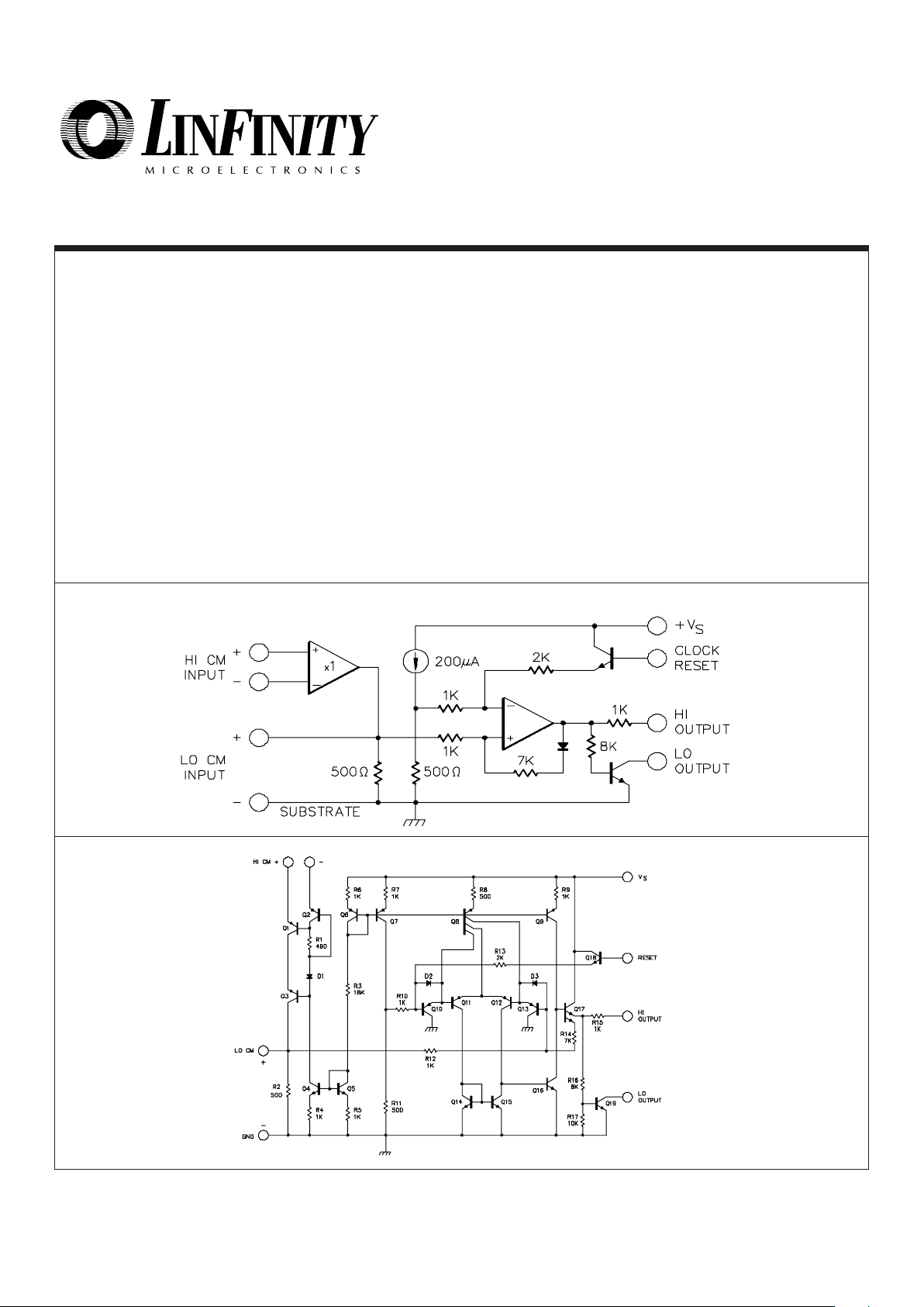
DESCRIPTION
This monolithic integrated circuit is an analog latch device with digital reset. It was
specifically designed to provide pulse-by-pulse current limiting for switch-mode power
supply systems, but many other application are also feasible. Its function is to provide
a latching switch action upon sensing an input threshold voltage, with reset accomplished by an external clock signal. This device can be interfaced directly with many
kinds of pulse width modulating control IC's, including the SG1524, SG1525A and
SG1527A.
The input threshold for the latch circuit is 100mV, which can be referenced either to
ground or to a wide-ranging positive voltage. There are high and low-going output
signals available, and both the supply voltage and clock signal can be taken directly
from an associated PWM control chip.
With delays in the range of 200 nanoseconds, this latch circuit is ideal for fast reaction
sensing to provide overall current limiting, short circuit protection, or transformer
saturation control.
FEATURES
••
••
• Current sensing with 100mV
threshold
••
••
• Common-mode input at ground or
to 40V
••
••
• Complementary outputs
••
••
• Automatic reset from PWM clock
••
••
• 180ns delay
••
••
• Interface direct to SG1524,
SG1525A, SG1527A
HIGH RELIABILITY FEATURES
- SG1549
♦♦
♦♦
♦ Available to MIL-STD-883
♦♦
♦♦
♦ LMI level "S" processing available
♦♦
♦♦
♦ Radiation data available
BLOCK DIAGRAM
SCHEMATIC
Page 2
4/90 Rev 1.1 2/94 LINFINITY Microelectronics Inc.
Copyright 1994 11861 Western Avenue
∞ ∞
∞ ∞
∞ Garden Grove, CA 92841
2 (714) 898-8121
∞∞
∞∞
∞ FAX: (714) 893-2570
Operating Junction Temperature
Hermetic (Y Package) ..................................................
Plastic (N Package) ......................................................
Storage Temperature Range ............................
150°C
150°C
-65°C to 150°C
Input Supply Voltage, VS .....................................................
HI CM Input Voltage ............................................................
LO Output "off" Voltage .......................................................
LO Output "on" current .....................................................
25V
40V
40V
25mA
ABSOLUTE MAXIMUM RATINGS (Note 1)
SG1549/SG2549/SG3549
Note 1. Values beyond which damage may occur.
Y Package:
Thermal Resistance-
Junction to Case, θ
JC
.................. 50°C/W
Thermal Resistance-
Junction to Ambient, θ
JA
............ 130°C/W
M Package:
Thermal Resistance-
Junction to Case, θ
JC
.................. 60°C/W
Thermal Resistance-
Junction to Ambient, θ
JA
............. 95°C/W
THERMAL DATA
Note A. Junction Temperature Calculation: TJ = TA + (PD x θJA).
Note B. The above numbers for
θJC are maximums for the limiting
thermal resistance of the package in a standard mounting configuration. The θ
JA
numbers are meant to be
guidelines for the thermal performance of the device/pcboard system. All of the above assume no ambient
airflow.
Min. Trigger Voltage
Input Current
2.0202.5
40
2.0
20
V
µA
VCM = 2V, Pin 3 open, TA = 25°C
V
CM
= 40V, Pin 3 open, TA = 25°C
V
CM
= 2V, Pin 3 open
V
CM
= 40V, Pin 3 open
V
PIN 1
= V
PIN 2
= 40V
Threshold Voltage
Input Current
100
100
500
500
80
70
400
300
80
70
400
300
120
130
600
700
100
100
500
500
120
130
600
700
mV
mV
Ω
Ω
SG3549SG1549/2549
Test ConditionsParameter Units
V
PIN 8
= 5V
V
PIN 8
= 20V
Supply Current
Supply Section
2103
15
2
10
Note 3. Input threshold voltages and supply current are directly proportional to supply voltage, VS .
5.0V
2V to 40V
5V to 40V
0 to 10mA
0V to 0.8V
Reset HI Voltage ....................................................
Operating Ambient Temperature Range
SG1549Y .......................................................
SG2549Y or M .................................................
SG3549Y or M ....................................................
2.5V to 5.0V
-55°C to 125°C
-25°C to 85°C
0°C to 70°C
Note 2. Range over which the device is functional.
Input Supply Voltage, VS ....................................................
HI CM Input Voltage ..................................................
LO Output "off" Voltage .............................................
LO Output "on" Current .............................................
Reset LO Voltage .....................................................
RECOMMENDED OPERATING CONDITIONS (Note 2)
ELECTRICAL CHARACTERISTICS
(Unless otherwise specified, these specifications apply over the operating ambient temperatures for SG1549 with -55° C ≤ TA ≤ 125°C, SG2549 with
-25°C ≤ TA ≤ 85°C, SG3549 with 0°C ≤ TA ≤ 70°C, and VS = 5V. Low duty cycle pulse testing techniques are used which maintains junction and case
temperatures equal to the ambient temperature.)
Min. Typ. Max. Min. Typ. Max.
515mA
mA
LO CM Input Section (Note 3)
Pin 1 & 2 shorted, TA = 25°C
pin 1 & 2 shorted
V
PIN 3
= 50mV, TA = 25°C
V
PIN 3
= 50mV
Threshold Voltage
Input Impedance
HI CM Input Section
(Note 3)
100
100
100
100
200
120
120
130
130
300
80
80
70
70
120
120
130
130
300
mV
mV
mV
mV
µA
100
100
100
100
200
80
80
70
70
Clock Reset Section
V
PIN 7
= 4V
2.5
40
Page 3

4/90 Rev 1.1 2/94 LINFINITY Microelectronics Inc.
Copyright 1994 11861 Western Avenue
∞ ∞
∞ ∞
∞ Garden Grove, CA 92841
3 (714) 898-8121
∞∞
∞∞
∞ FAX: (714) 893-2570
LO Output
1.0
0.5
.01.31.0
0.5
V
PIN 5
= 40V
I
L
= 5mA
Off Leakage
On Voltage
SG1549/SG2549/SG3549
TYPICAL SWITCHING CHARACTERISTICS (Note 4)
(VS = 5V, TA = 25°C)
Reset Minimum Pulse Width (TW1)
Delay from Reset to LO Output (T
D(OFF)
)
LO Input Minimum Pulse Width (T
W2
)
Delay from LO Input to LO Output (T
D(ON)
)
Delay from HI Input to LO Output (T
D(ON)
)
Delay from HI Output to LO Output
ns
ns
ns
ns
ns
ns
300
600
300
360
900
60
150
300
50
180
300
30
Min. Typ. Max.
SG1549 Series
Test ConditionsParameter Units
DYNAMIC TEST CIRCUIT
SWITCHING WAVEFORMS
APPLICATION NOTES
HIGH LINE SENSING - The SG1549 will provide current sensing in the
positive supply line in the typical SG1524 single-ended switching
regulator application shown in Figure 1. The HI CM sense circuitry can
be used with input voltages between 2 and 40 volts.
A value for RSC is determined by dividing the 100mV input threshold by
the peak current desired. High-frequency noise, or switching transients,
can usually be eliminated by a small capacitor between pins 3 and 4.
Current control may be accomplished by either the HI OUTPUT pin
connected to the SG1524’s Shutdown pin, or the LO OUTPUT pin
connected directly to the Compensation Terminal. In either case,
activation of the current sense latch will tend to discharge the compensation capacitor, C
C
, which may cause slow recovery from pulse limiting.
If this feature is desired, the LO OUTPUT pin may be used to discharge
a soft-start network instead of coupling directly to the SG1524. If it is not
desired, the use of a small value of C
C
, and perhaps a diode across RC,
will enhance recovery.
ELECTRICAL CHARACTERISTICS
(VS = 5V, and over recomended operating temperature, unless otherwise specified.)
Min. Typ. Max.
Min. Typ. Max.
SG3549SG1549/2549
Test ConditionsParameter Units
Amplitude = 3.0V
R
L
= 470Ω to V
S
LO CM Amplitude = 200mV
LO CM Amplitude = 200mV, R
L
= 470Ω to V
S
Amplitude = 200mV, VCM = 5V
LO CM Input = 200mV
Off Voltage
On Voltage
0
3.2
0.1 V
V
0
3.2
0.1
I
L
= 1mA 2.8
Note 4: These parameters, although guaranteed, are not tested in production.
FIGURE 1 — HIGH LINE SENSING WITH THE SG1549 IN CONJUNCTION
WITH AN SG1524 PWM CONTROL IC
HI Output Section
2.8
.01
.3
µA
V
Page 4

4/90 Rev 1.1 2/94 LINFINITY Microelectronics Inc.
Copyright 1994 11861 Western Avenue
∞ ∞
∞ ∞
∞ Garden Grove, CA 92841
4 (714) 898-8121
∞∞
∞∞
∞ FAX: (714) 893-2570
SG1549/SG2549/SG3549
APPLICATION NOTES (continued)
FIGURE 2 — CURRENT CONTROL FOR A BUCK REGULATOR WITH
CONSTANT DRIVE CURRENT
FIGURE 4 — POWER BOOST AND CURRENT CONTROL WITH THE SG1627
FIGURE 3 — A PUSH-PULL CONVERTER WITH LOW-LINE
EMITTER CURRENT SENSING
Another method of introducing the current shutdown signal is shown in
Figure 2 where the SG1524 is used to activate a constant drive current
to the high-current switch, in this case an SM600. The 2N2222 forms a
constant current generator when driven from the SG1524’s 5.0 volt
reference through a 1K resistor. This transistor is then switched off by
the LO OUTPUT transistor in the SG1549, achieving the fastest response to the output of the regulator.
LOW LINE SENSING - In many types of feed-forward or push-pull
converters, current protection may be provided by sensing in an emitter
resistor referenced to ground on the primary side of an output transformer. The fast-reacting SG1549 can easily sense secondary overload
as reflected back to the primary and, additionally, provide protection
from unbalanced transformer saturation.
When using the LO CM inputs, the HI CM inputs should be shorted
together. While the LO CM inputs may be connected directly across a
sense resistor, R
SC
, a small low-pass filter as shown in Figure 3 is often
required to eliminate high frequency transients. It must be remembered
that the 500Ω input impedance at the LO CM terminals will cause the use
of R1 to increase the effective threshold; however, this also offers the
possibility of an easily adjustable threshold by incorporating a potentiometer at the input.
Coupling the output signal from the SG1549 to the control chip may be
done in several ways including the use of either the Compensation or
Shutdown pins on the SG1524 as described earlier.
Another convenient way to tie the output of the SG1549 into the PWM
control in higher power applications is by using the SG1627 Dual
Interface Driver and connecting the LO OUTPUT terminal of the Sg1549
directly to the two Non-Inverting inputs of the SG1627 as shown in Figure
4.
And finally, keep in mind that the LO OUTPUT terminal of the SG1549
will easily drive most high-speed optical couplers should some type of
isolation between current sense and shutdown control be required.
Ambient
Temperature Range
Part No.Package Connection Diagram
8-PIN CERAMIC DIP
Y - PACKAGE
8
7
6
5
2
1
3
4
— HI CM INPUT
+ HI CM INPUT
+ LO CM INPUT
— LO CM INPUT
CLOCK RESET
+V
S
LO OUTPUT
HI OUTPUT
SG1549Y/883B -55°C to 125°C
SG1549Y/DESC -55°C to 125°C
SG1549Y -55°C to 125°C
SG2549Y -25°C to 85°C
SG3549Y 0°C to 70°C
CONNECTION DIAGRAMS & ORDERING INFORMATION (See Notes Below)
8-PIN PLASTIC DIP
M - PACKAGE
SG2549M -25°C to 85°C
SG3549M 0°C to 70°C
Note1. Contact factory for JAN and DESC product availability. 2. All parts are viewed from the top.
 Loading...