

Datasheet SG1544J, SG1544J-883B, SG1544J-DESC, SG2544DW, SG2544J Datasheet (Microsemi Corporation)
...Page 1
SG1544/SG2544/SG3544
4/90 Rev 1.1 2/94 LINFINITY Microelectronics Inc.
Copyright 1994 11861 Western Avenue
∞ ∞
∞ ∞
∞ Garden Grove, CA 92841
1 (714) 898-8121
∞∞
∞∞
∞ FAX: (714) 893-2570
LOW-VOLTAGE SUPERVISORY CIRCUIT
FEATURES
••
••
• Uncommitted comparator inputs for
wide input flexibility
••
••
• Common-Mode range from zero to near
supply voltage
••
••
• Reference voltage trimmed to 1%
accuracy
••
••
• Over-voltage, under-voltage, and current
sensing circuits all included
••
••
• SCR "Crowbar" drive of 300mA
••
••
• Programmable time delays
••
••
• Open-collector outputs and remote
activation capability
••
••
• Total standby current less than 10mA
HIGH RELIABILITY FEATURES
- SG1544
♦♦
♦♦
♦ Available to MIL-STD-883 and DESC
SMD
♦♦
♦♦
♦ LMI level "S" processing available
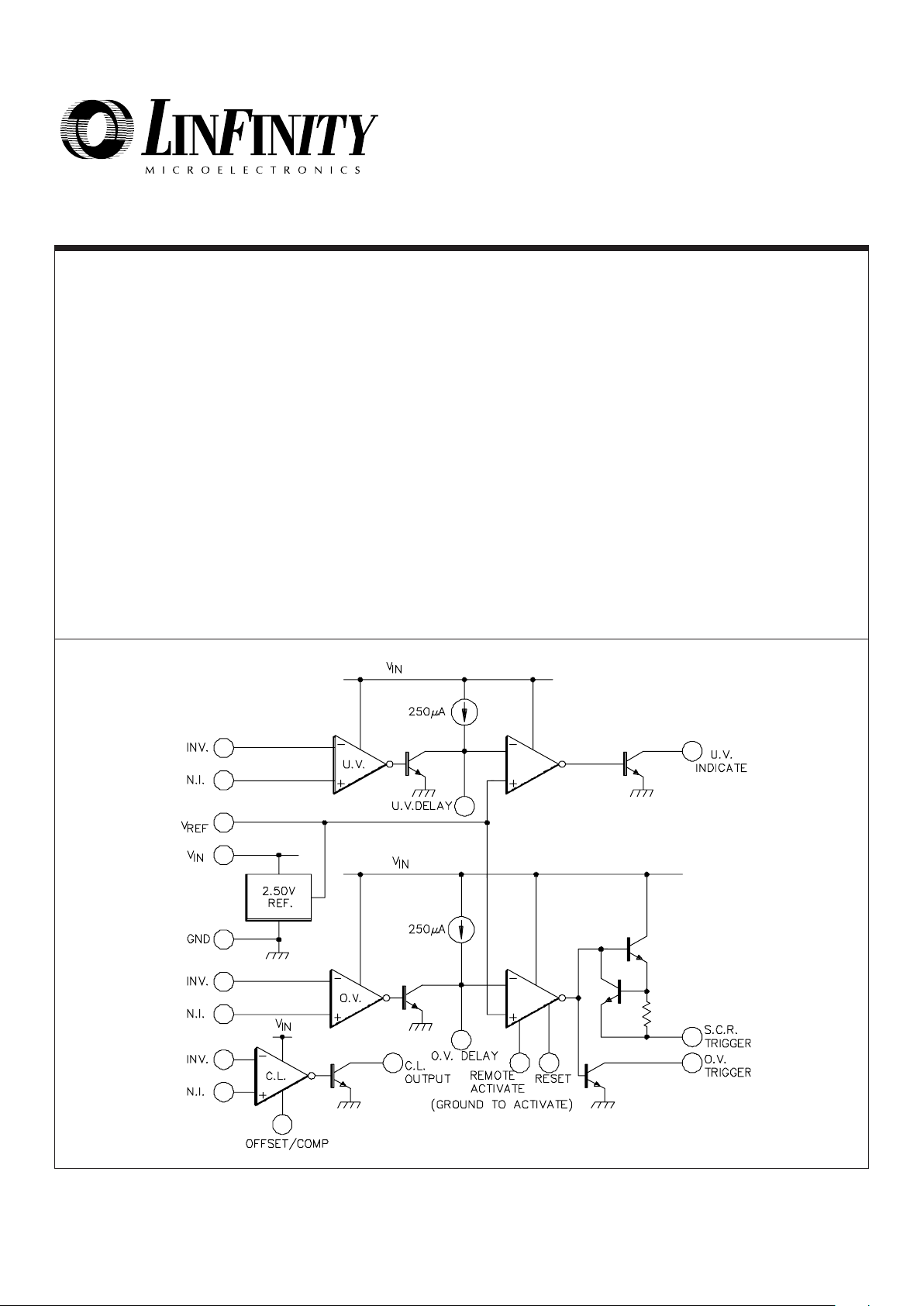
DESCRIPTION
This device was designed to provide all the operational features of the SG1543/
2543/3543 devices but with the added advantage of uncommitted inputs to the
voltage sensing comparators. This allows monitoring of voltage levels less than
2.5 volts by dividing down the internal reference supply.
In all other respects, the SG1544 series is identical to the SG1543 series. These
monolithic devices contain all the functions necessary to monitor and control the
output of a sophisticated power supply system. Over-voltage sensing with
provision to trigger an external SCR “crowbar” shutdown; an under-voltage circuit
which can be used to monitor either the output or sample the input line voltage;
and a third op amp/comparator usable for current sensing are all included in this
IC, together with an independent, accurate reference generator.
The voltage-sensing input comparators are identical and can be used with
threshold levels from zero volts to (V
IN
- 3V). Each has approximately 25mv of
hysteresis which is offset so the switching differential threshold is zero on the noninverting input for rising levels and zero on the inverting input for falling signals.
All other operating characteristics are as described in the SG1543 data sheet and
application note.
BLOCK DIAGRAM
Page 2
SG1544/SG2544/SG3544
4/90 Rev 1.1 2/94 LINFINITY Microelectronics Inc.
Copyright 1994 11861 Western Avenue
∞ ∞
∞ ∞
∞ Garden Grove, CA 92841
2 (714) 898-8121
∞∞
∞∞
∞ FAX: (714) 893-2570
Note 1. Values beyond which damage may occur.
Note 2. At higher input voltages, a dissipation limiting resistor, RG , is required. See Figure 1.
ABSOLUTE MAXIMUM RATINGS (Note 1)
Indicator Output Sink Current ..........................................
Operating Junction Temperature
Hermetic (J Package) ..................................................
Plasitc (N, DW Packages) .......................................
Storage Temperature Range ............................
50mA
150°C
150°C
-65°C to 150°C
Input Supply Voltage (+VIN) ................................................
Sense Inputs ......................................................................
SCR Trigger Current
(Note 2) .........................................
Indicator Output Voltage .....................................................
40V
+V
IN
300mA
40V
J Package:
Thermal Resistance-
Junction to Case, θ
JC
.................. 25°C/W
Thermal Resistance-
Junction to Ambient, θ
JA
.............. 70°C/W
N Package:
Thermal Resistance-
Junction to Case, θ
JC
.................. 30°C/W
Thermal Resistance-
Junction to Ambient, θ
JA
............. 60°C/W
DW Package:
Thermal Resistance-
Junction to Case, θ
JC
.................. 35°C/W
Thermal Resistance-
Junction to Ambient, θ
JA
............. 90°C/W
Input Supply Voltage (+V
IN
) ....................................
Current Limit Common Mode
Input Voltage Range .......................................
Reference Load Current ...........................................
Indicator Output Voltage ........................................
Indicator Output Current ...........................................
4.7V to 40V
0V to +V
IN
-3V
0 to 10mA
4.7V to 40V
0 to 10mA
Delay Timing Capcitor
(Note 4) .....................................
Operating Ambient Temperature Range
SG1544 .........................................................
SG2544 ...........................................................
SG3544 ..............................................................
0 to 1µF
-55°C to 125°C
-25°C to 85°C
0°C to 70°C
Note 3: Range over which the device is functional.
Note 4. Larger value capacitor may be used with peak current limiting. See Figure 1.
RECOMMENDED OPERATING CONDITIONS (Note 3)
ELECTRICAL CHARACTERISTICS
(Unless otherwise specified, these specifications apply over the operating ambient temperatures for SG1544 with -55°C ≤ TA ≤ 125°C, SG2544 with
-25°C ≤ TA ≤ 85°C, SG3544 with 0°C ≤ TA ≤ 70°C, and +VIN = 10V. Indicator outputs have 2kΩ pull-up resistors. All electrical ratings and specifications
are tested with the inverting over-voltage input and the non-inverting under-voltage input externally connected to the 2.5V reference. Low duty cycle
testing techniques are used which maintains junction and case temperatures equal to the ambient temperature.)
7
40
40
10
4.5
4.7
Supply Section
T
J
= 25°C to T
MAX
+VIN = 40V, Outputs open
Input Voltage Range
Supply Current
SG3544SG1544/2544
UnitsTest ConditionsParameter
2.50
1
1
25
.005
2.48
2.45
12
Reference Section
T
J
= 25°C
+V
IN
= 5 to 30V
I
REF
= 0 to 10mA
V
REF
= 0V
Output Voltage
Line Regulation
Load Regulation
Short Circuit Current
Temperature Stability
V
V
mV
mV
mA
%/°C
V
V
mA
40
40
107
4.5
4.7
Min. Typ. Max.Min. Typ. Max.
2.55
2.60
5
10
40
2.50
1
1
25
.005
2.45
2.40
12
2.52
2.55
5
10
40
THERMAL DATA
Note A. Junction Temperature Calculation: TJ = TA + (PD x θJA).
Note B. The above numbers for θ
JC
are maximums for the limiting
thermal resistance of the package in a standard mounting configuration. The θ
JA
numbers are meant to be
guidelines for the thermal performance of the device/pcboard system. All of the above assume no ambient
airflow.
Page 3

SG1544/SG2544/SG3544
4/90 Rev 1.1 2/94 LINFINITY Microelectronics Inc.
Copyright 1994 11861 Western Avenue
∞ ∞
∞ ∞
∞ Garden Grove, CA 92841
3 (714) 898-8121
∞∞
∞∞
∞ FAX: (714) 893-2570
The 100 ohm resistor limits the peak discharge current into the SG1544 while the external PNP transistor provides a high peak-current
discharge path for the delay capacitor.
FIGURE 1 - SURGE LIMIT CIRCUIT FOR LARGE DELAY CAPACITORS
SG1544
0
80
60
72
OFFSET/COMP pin open, V
CM
= 0V
OFFSET/COMP pin open, V
CM
= 0V
10Ω from OFFSET/COMP pin to Gnd,
TJ = 25°C
0 ≤ VCM ≤ 12V, VIN = 15V
OFFSET/COMP pin open, V
CM
= 0V
I
L
= 10mA
V
IND
= 40V
A
V
= 0dB, TJ = 25°C
V
OVERDRIVE
= 100mV, TJ = 25°C
Input Voltage Range
Input Bias Current
Input Offset Voltage
CMRR
AVOL
Output Saturation
Output Leakage
Small Signal Bandwidth
Propagation Delay
0.3
0
100
70
80
0.2
.01
5
200
+VIN = 5V, RG = 0, VO = 0
+V
IN
= 15V, IO = 100mA
+V
IN
= 40V, RL = 1KΩ
REM. ACT. pin = Gnd
REM. ACT pin open
RESET pin = Gnd, REM. ACT. = Gnd
RESET pin open, REM. ACT. = Gnd
RL = 50Ω, TJ = 25°C, CD = 0
V
REM. ACT.
= 0.4V
V
O.V. N.I. INPUT
= 2.7V
Peak Output Current
Peak Output Voltage
Output Off Voltage
Remote Activate Current
Remote Activate Voltage
Reset Current
Reset Voltage
Output Current Rise Time
Prop. Delay from REM. ACT. Pin
Prop. Delay fom O.V. N.I. IN Pin
200
13
0
0.4
2
0.4
2
400
300
500
100
12
ELECTRICAL CHARACTERISTICS (continued)
2.45
2.40
200
Comparator Section
T
J
= 25°C
Sense input = 0V
V
D
= 0V
I
L
= 10mA
V
IND
= 40V
V
O.V. N.I. IN
= 2.7V, V
U.V. INV. IN
= 2.3V, TJ = 25°C
C
D
= 0
C
D
= 1µF
Input Threshold (Note 5)
Input Hysteresis
Input Bias Current
Delay Saturation
Delay High Level
Delay Charging Current
Indicate Saturation
Indicate Leakage
Propagation Delay
UnitsTest ConditionsParameter
SCR Trigger Section
2.50
25
0.3
0.2
6
250
0.2
.01
400
10
VIN-3V
1.0
10
120
0.5
1.0
APPLICATION INFORMATION
SG1544/2544 SG3544
Min. Typ. Max. Min. Typ. Max.
2.55
2.60
1.0
0.5
8
300
0.5
1.0
2.40
2.35
200
2.50
25
0.3
0.2
6
250
0.2
0.1
400
10
2.60
2.65
1.0
0.5
8
300
0.5
1.0
V
V
mV
µA
V
V
µA
V
µA
ns
ms
mA
V
V
mA
V
mA
V
mA/µs
ns
ns
400
0.1
0.8
6
0.8
6
200
13
0
0.4
2
0.4
2
400
300
500
100
12
400
0.1
0.8
6
0.8
6
Current Limit Section
0
70
60
72
0.3
0
100
70
80
0.2
.01
5
200
VIN-3V
1.0
15
130
0.5
1.0
V
µA
mV
mV
dB
dB
V
µA
MHz
ns
Note 5. Input voltage rising on O.V. N.I. INPUT and falling on U.V. INV. INPUT.
Page 4

SG1544/SG2544/SG3544
4/90 Rev 1.1 2/94 LINFINITY Microelectronics Inc.
Copyright 1994 11861 Western Avenue
∞ ∞
∞ ∞
∞ Garden Grove, CA 92841
4 (714) 898-8121
∞∞
∞∞
∞ FAX: (714) 893-2570
CONNECTION DIAGRAMS & ORDERING INFORMATION (See Notes Below)
Ambient
Temperature Range
Part No.Package
Connection Diagram
10
1
2
3
4
5
6
7
8
9
16
15
14
13
12
11
17
18
18-PIN CERAMIC DIP
J - PACKAGE
SG1544J/883B -55°C to 125°C
SG1544JDESC -55°C to 125°C
SG1544J -55°C to 125°C
SG2544J -25°C to 85°C
SG3544J 0°C to 70°C
SG2544N -25°C to 85°C
SG3544N 0°C to 70°C
18-PIN PLASTIC DIP
N - PACKAGE
U.V. N.I. INPUT
RESET
REMOTE ACTIVATE
SCR TRIGGER
OFFSET / COMP
C.L. N.I. INPUT
C.L. OUTPUT
U.V. DELAY
U.V. INDICATE
C.L. INV. INPUT
GROUND
O.V. INDICATE
U.V. INV. INPUT
O.V. DELAY
O.V. N.I. INPUT
O.V. INV. INPUT
1
18-PIN WIDE BODY
PLASTIC S.O.I.C.
DW - PACKAGE
SG2544DW -25°C to 85°C
SG3544DW 0°C to 70°C
16
15
14
13
12
11
10
17
18
2
3
4
5
6
7
8
9
+V
IN
V
REF
OFFSET / COMP
C.L. N.I. INPUT
C.L. OUTPUT
U.V. DELAY
U.V. INDICATE
C.L. INV. INPUT
GROUND
+V
IN
V
REF
U.V. N.I. INPUT
RESET
REMOTE ACTIVATE
SCR TRIGGER
O.V. INDICATE
U.V. INV. INPUT
O.V. DELAY
O.V. N.I. INPUT
O.V. INV. INPUT
Note 1. Contact factory for JAN and DESC product availablity.
2. All packages are viewed from the top.
 Loading...