

Datasheet SG1540Y-883B, SG2540DW, SG2540M, SG2540Y, SG3540DW Datasheet (Microsemi Corporation)
...Page 1
SG1540/SG2540/SG3540
OFF-LINE START-UP CONTROLLER
DESCRIPTION
The SG1540 is an integrated circuit designed to efficiently provide
start-up power from a high-voltage DC bus to a PWM control circuit
in a switching power supply. When used on the primary side, it
reduces start-up current to less than 1mA and allows any standard
PWM control circuit to be used as a primary-side controller. When
used to power a controller on the secondary side, it efficiently
eliminates the need for a heavy 50/60Hz line transformer with its
associated low frequency magnetic fields.
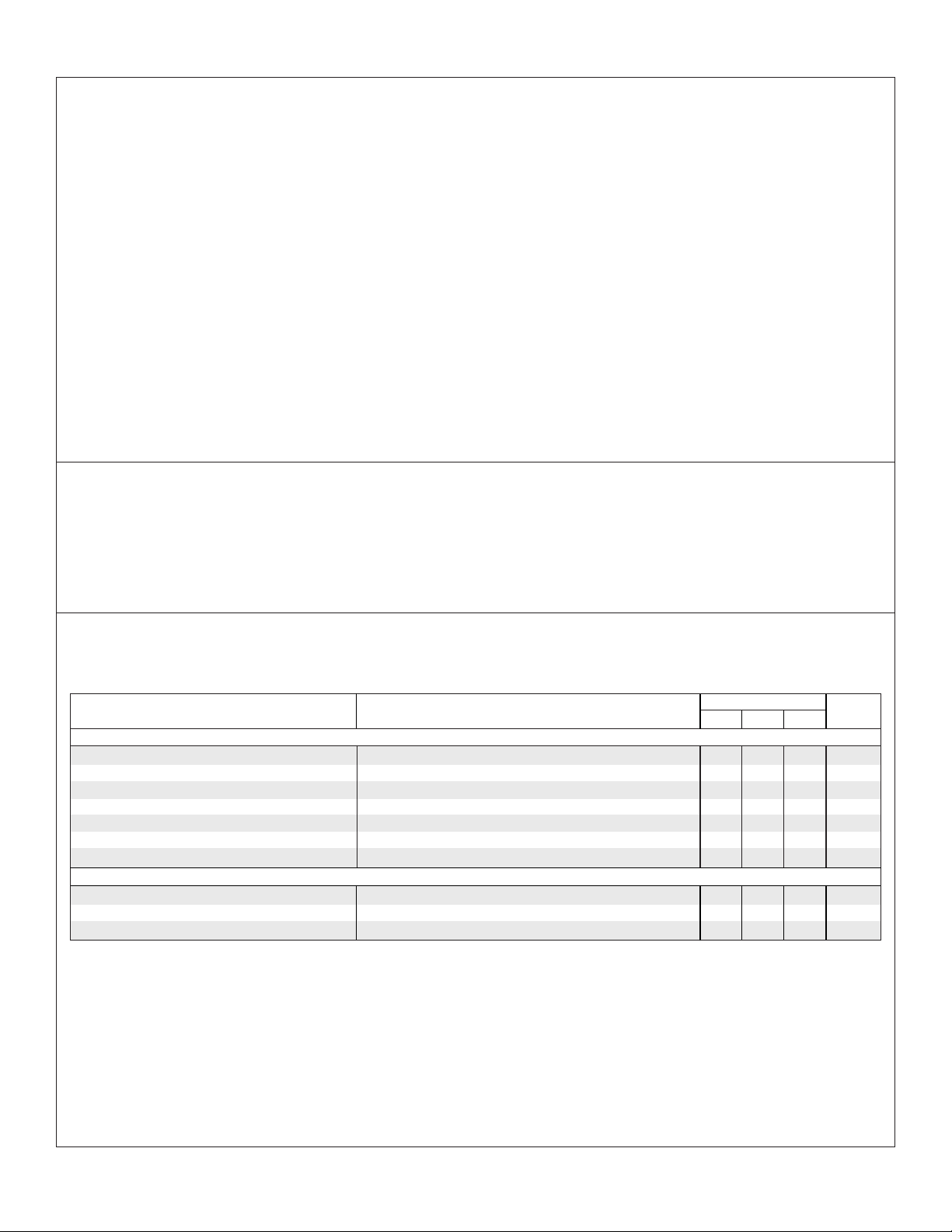
The circuit consists of three sections: a micropower bandgap
comparator/power switch referenced to 2.5 volts which isolates the
start-up capacitor from its load; a high frequency square-wave
oscillator with 200mA totem-pole output for driving an isolation
transformer; and a second bandgap comparator with latching
crowbar to protect against overvoltage faults while starting or
running.
The SG1540 is specified for operation over the full military ambient
temperature range of -55°C to 125°C. The SG2540 is characterized for the industrial range of -25°C to 85°C, and the SG3540 is
designed for the commercial range of 0°C to 70°C.
BLOCK DIAGRAM
FEATURES
••
• Useable with primary and secondary side PWM
••
controllers
••
• Micropower comparator / switch
••
- Internal 2.5V bandgap reference
- 50mA power switch
••
• Squarewave oscillator
••
- 500Hz to 200KHz operation
- 200mA totem pole outputs
••
• Eliminates bulky, expensive 50/60 Hz transformer
••
••
• Minimizes high voltage bleeder current
••
••
• Programmable start-up voltage and hysteresis
••
••
• Internal and programmable overvoltage crowbar
••
latch
••
• Available in 8 pin DIP, 10 pin flat pack, and 16 pin
••
widebody SOIC
HIGH RELIABILITY FEATURES - SG1540
♦♦
♦ Available to MIL-STD - 883
♦♦
♦♦
♦ LMI level "S" processing available
♦♦
4/90 Rev 1.1 2/94 LINFINITY Microelectronics Inc.
Copyright 1994 11861 Western Avenue
1 (714) 898-8121
∞ ∞
∞ Garden Grove, CA 92841
∞ ∞
∞∞
∞ FAX: (714) 893-2570
∞∞
Page 2
ABSOLUTE MAXIMUM RATINGS (Note 1)
Supply Voltage (+V
DC Output Current, Continuous (V
AC Output Current, Continuous ..................................... 200mA
Analog Inputs (Start and Overvoltage) .................-0.3V to 6.0V
Analog Input Currents (V>8V).......................................... 10mA
Overvoltage Crowbar Current, Continuous ..................... 50mA
Note 1. Values beyond which damage may occur.
)........................................................ +37V
IN
)........................... 100mA
OUT
THERMAL DATA
Y Package:
Thermal ResistanceThermal Resistance-
M Package:
Thermal ResistanceThermal Resistance-
DW Package:
Thermal ResistanceThermal Resistance-
Junction to Case, θ
Junction to Ambient, θ
Junction to Case, θ
Junction to Ambient, θ
Junction to Case, θ
Junction to Ambient, θ
JC
JC
JC
.................. 50°C/W
............ 130°C/W
JA
.................. 60°C/W
............. 95°C/W
JA
.................. 40°C/W
............. 95°C/W
JA
RECOMMENDED OPERATING CONDITIONS (Note 2)
Supply Voltage Range ............................................... 7V to 35V
DC Output Current, Continuous................................ 0 to 50mA
AC Output Current, Continuous ............................. 0 to 100 mA
Oscillator Frequency Range ........................... 1KHz to 400KHz
Timing Resistor Range ...................................... 2KΩ to 150KΩ
Note 2. Range over which the device is functional.
SG1540/SG2540/SG3540
Overvoltage Crowbar Energy (½CV²)................................. 8mJ
Operating Junction Temperature
Hermetic (Y Package) ................................................ 150°C
Plastic (M, DW Packages) .......................................... 150°C
Storage Temperature Range ............................ -65°C to 150°C
Lead Temperature (Soldering, 10 Seconds) .................. 300°C
Note A. Junction Temperature Calculation: TJ = TA + (PD x θJA).
Note B. The above numbers for θ
thermal resistance of the package in a standard mounting configuration. The θ
guidelines for the thermal performance of the device/pcboard system. All of the above assume no ambient
airflow.
Timing Capacitor Range ........................................ 1nF to 20µF
Operating Ambient Temperature Range
SG1540 ...........................................................-55°C to 125°C
SG2540 .............................................................-25°C to 85°C
SG3540 ................................................................ 0°C to 70°C
are maximums for the limiting
JC
numbers are meant to be
JA
ELECTRICAL CHARACTERISTICS
(Unless otherwise specified, these specifications apply over the operating ambient temperatures for SG1540 with -55°C ≤ TA ≤ 125°C, SG2540 with
-25°C ≤ TA ≤ 85°C, SG3540 with 0°C ≤ TA ≤ 70°C, and +VIN = 15V. A 0.1µF high frequency bypass capacitor is recommended on VIN. Low duty cycle
testing techniques are used which maintains junction and case temperatures equal to the ambient temperature.)
SG1540/2540/3540
Min.
Typ. Max.
0.2
0.4
0.3
0.6
3
6
2.37
2.50
2.63
6
12.5
12.0
50
0.1
0.1
13.5
13.0
100 225
1
7
8
0.2
Units
mA
mA
mA
V
µA
V
V
V
V
mA
Start-up Section
Start Current I
CC
Operating Current
Start Threshold
Start Bias Current
Start Clamp Voltage
Hysteresis ON Voltage
DC Output Section
Voltage
V
OUT
Short Circuit Current
V
= 0 to 2.37V
START
V
TIMING
F
= 50KHz, V
OSC
= 0 to 5V
V
PIN 1
I
= 1mA
PIN 1
= 100µA
I
PIN 4
I
SOURCE
I
SOURCE
V
= 0V
OUT
= +VIN; V
= 10mA
= 50mA
Test ConditionsParameter
Open
OUT
and AC
OUT
OUT
Open
4/90 Rev 1.1 2/94 LINFINITY Microelectronics Inc.
Copyright 1994 11861 Western Avenue
2 (714) 898-8121
∞ ∞
∞ Garden Grove, CA 92841
∞ ∞
∞∞
∞ FAX: (714) 893-2570
∞∞
Page 3

ELECTRICAL CHARACTERISTICS (continued)
SG1540/SG2540/SG3540
Parameter Units
Test Conditions
Oscillator Section (Note 3)
Initial Accuracy
Voltage Stability
Temperature Stability
(Note 4)
Oscillator Minimum Frequency
Oscillator Maximum Frequency
TJ = 25°C
+V
= 12 to 18V
IN
= 17.8K, CT = .068µF
R
T
R
= 1.5K, CT = 470pF
T
AC Output Section
I
HIGH Output Voltage
LOW Output Voltage
Squarewave Duty Cycle
AC Output Risetime
AC Output Falltime
SOURCE
I
SOURCE
= 20mA
I
SINK
I
= 100mA
SINK
= 1000pF
C
L
C
= 1000pF
L
= 20mA
= 100mA
Overvoltage Crowbar Section
Overvoltage Threshold
Overvoltage Bias Current
Overvoltage Clamp Voltage
+V
Overvoltage Threshold
IN
SCR ON Voltage
SCR Holding Current
Note 3. F
Note 4. These parameters, although guaranteed, are not tested in production.
= 50KHz, RT = 3.48K CT = 4.7nF unless otherwise specified.
OSC
V
= 0 to 2.37V
O.V.
= 1mA
I
O.V.
= 35mA
I
VIN
V
= 0
O.V.
SG1540/2540/3540
Min. Typ. Max.
46
50
54
5
12
2
5
1
400
13.5
12.5
13.0
12.0
0.3
0.2
2.0
1.2
50
45
2.37
6
37
0.15
2.50
0.35
0.3
0.1
0.1
42
55
0.6
0.2
2.63
1
7
8
44
9
12
0.55
KHz
%
%
KHz
KHz
V
V
V
V
%
µS
µS
V
µA
V
V
V
mA
CHARACTERISTIC CURVES
FIGURE 1 - SATURATION VOLTAGE (DC OUT PIN) VS. OUTPUT CURRENT
FIGURE 2 - OSCILLATOR FREQUENCY VS. RT AND C
T
4/90 Rev 1.1 2/94 LINFINITY Microelectronics Inc.
Copyright 1994 11861 Western Avenue
3 (714) 898-8121
∞ ∞
∞ Garden Grove, CA 92841
∞ ∞
∞∞
∞ FAX: (714) 893-2570
∞∞
Page 4

SG1540/SG2540/SG3540
APPLICATION INFORMATION
FIGURE 3 - EFFICIENT PRIMARY SIDE START-UP
PRIMARY SIDE START-UP
When the design goal is efficient start-up for a control PWM referenced to the primary side of the power transformer, the configuration
in Figure 3 is recommended. An energy storage capacitor C
The value of R
C
ramps up from zero, the only load current is the standby current of the SG1540 and that of the divider network R1-R3. (Connecting
START
the TIMING pin to +V
bias current at the START pin is 1µA maximum, a divider current of 100µA is adequate).
is chosen to provide a constant 1mA charging current, allowing the use of a ½ watt resistor. As the voltage on
START
disables the internal power oscillator and forces the circuitry into a micropower standby model. Since the input
IN
is trickle-charged from the 300-400 Volt DC bus by resistor R
START
START
.
When the voltage at the START pin reaches +2.5 Volts, the hysteresis transistor turns off, overdriving the START pin. The V
is switched to the HIGH state, providing power to the PWM control circuit. As energy flows out of the START capacitor, its voltage
decays; but it remains connected to the PWM circuit until the dropout voltage is reached (V
on the power transformer and rectifier diode D5 prevent this from happening. As the PWM control circuit becomes active, the power
START
- V
HYSTERESIS
). The bootstrap winding
OUT
pin
transistor begins to switch, providing operating current to the PWM circuit through the SG1540.
RESISTOR CALCULATIONS
Given that V
are calculated as follows:
1. For simplification, let X =
START
and V
have been chosen, and that the divider current at start-up is 100µA, then the values for R1 through R3
DROPOUT
V
- 2.5
and Y =
START
V
DROPOUT
2.5
2.5
-2.5
2. Then,R1 = 2.5 x 10
R2 = R1/Y [2]
and R3 = [3]
4
* X [1]
R1 * R2
X * R2 - R1
DESIGN EXAMPLE
Suppose we have a power MOSFET device, and so want to start at +18 volts and drop out at +12 volts.
Then X = 6.20
and Y = 3.80
4
Therefore R1 = 2.5 x 10
R2 = 1.5 x 10
R3 = = 63.7K (Choose 62K)
6.2 * 3.9 x 104 - 1.5 x 10
* 6.2 = 155K (Choose 150K)
5
/3.8 = 39.5K (Choose 39K)
1.5 x 105 * 3.9 x 10
4
5
4/90 Rev 1.1 2/94 LINFINITY Microelectronics Inc.
Copyright 1994 11861 Western Avenue
4 (714) 898-8121
∞ ∞
∞ Garden Grove, CA 92841
∞ ∞
∞∞
∞ FAX: (714) 893-2570
∞∞
Page 5

APPLICATIONS INFORMATION (continued)
The voltage waveform at +VIN is shown in Figure 4 with these resistor values and with C
before the +15 volt bootstrap winding becomes active.
SG1540/SG2540/SG3540
= 3µF. Notice that two tries are required
START
FIGURE 4 - STARTUP VOLTAGE WAVEFORM
FIGURE 5 - SECONDARY-SIDE START-UP WITHOUT A LINE TRANSFORMER
4/90 Rev 1.1 2/94 LINFINITY Microelectronics Inc.
Copyright 1994 11861 Western Avenue
5 (714) 898-8121
∞ ∞
∞ Garden Grove, CA 92841
∞ ∞
∞∞
∞ FAX: (714) 893-2570
∞∞
Page 6

CONNECTION DIAGRAMS & ORDERING INFORMATION (See Notes Below)
SG1540/SG2540/SG3540
8-PIN CERAMIC DIP
Y - PACKAGE
8-PIN PLASTIC DIP
M - PACKAGE
16-PIN WIDE BODY
PLASTIC S.O.I.C.
DW - PACKAGE
Part No.Package
Ambient
Temperature Range
SG1540Y/883B -55°C to 125°C
SG1540Y -55°C to 125°C
SG2540Y -25°C to 85°C
SG3540Y 0°C to 70°C
SG2540M -25°C to 85°C
SG3540M 0°C to 70°C
SG2540DW -25°C to 85°C
SG3540DW 0°C to 70°C
Connection Diagram
START
OVER VOLTAGE
HYSTERESIS
TIMING
START
N.C.
OVER VOLTAGE
N.C.
HYSTERESIS
N.C.
TIMING
N.C.
8
1
2
3
4
1
2
3
4
5
6
7
8
7
6
5
16
15
14
13
12
11
10
DC OUT
+V
AC OUT
GROUND
9
IN
DC OUT
N.C.
+V
N.C.
AC OUT
N.C.
GROUND
N.C.
IN
Notes: 1. Contact factory for JAN and DESC part availability.
2. All parts are viewed from the top.
4/90 Rev 1.1 2/94 LINFINITY Microelectronics Inc.
Copyright 1994 11861 Western Avenue
6 (714) 898-8121
∞ ∞
∞ Garden Grove, CA 92841
∞ ∞
∞∞
∞ FAX: (714) 893-2570
∞∞
 Loading...