

Datasheet SG1526J, SG1526J-883B, SG1526L, SG1526L-883B, SG2526DW Datasheet (Microsemi Corporation)
...Page 1
SG1526/SG2526/SG3526
REGULATING PULSE WIDTH MODULATOR
DESCRIPTION
The SG1526 is a high performance monolithic pulse width modulator
circuit designed for fixed-frequency switching regulators and other
power control applications. Included in an 18-pin dual-in-line package
are a temperature compensated voltage reference, sawtooth oscillator,
error amplifier, pulse width modulator, pulse metering and steering logic,
and two low impedance power drivers. Also included are protective
features such as soft-start and undervoltage lockout, digital current
limiting, double pulse inhibit, a data latch for single pulse metering,
adjustable deadtime, and provision for symmetry correction inputs. For
ease of interface, all digital control ports are TTL and B-series CMOS
compatible. Active LOW logic design allows wired-OR connections for
maximum flexibility. This versatile device can be used to implement
single-ended or push-pull switching regulators of either polarity, both
transformerless and transformer coupled. The SG1526 is characterized
for operation over the full military ambient junction temperature range of
-55°C to +150°C. The SG2526 is characterized for operation from -25°C
to +150°C, and the SG3526 is characterized for operation from 0°C to
+125°C.
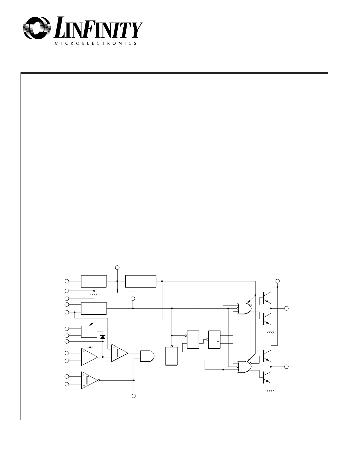
BLOCK DIAGRAM
FEATURES
••
• 8 to 35 volt operation
••
••
• 5V reference trimmed to ±1%
••
••
• 1Hz to 350KHz oscillator range
••
••
• Dual 100mA source/sink outputs
••
••
• Digital current limiting
••
••
• Double pulse suppression
••
••
• Programmable deadtime
••
••
• Undervoltage lockout
••
••
• Single pulse metering
••
••
• Programmable soft-start
••
••
• Wide current limit common mode range
••
••
• TTL/CMOS compatible logic ports
••
••
• Symmetry correction capability
••
••
• Guaranteed 6 unit synchronization
••
HIGH RELIABILITY FEATURES - SG1526
♦♦
♦ Available to MIL-STD-883B and DESC SMD
♦♦
♦♦
♦ Radiation data available
♦♦
♦♦
♦ LMI level "S"processing available
♦♦
+V
GROUND
RESET
C
SOFTSTART
COMPENSATION
+ ERROR
— ERROR
+ C.S.
— C.S.
V
REF
+V
IN
R
D
R
T
C
T
Reference
Regulator
Oscillator
Soft
Start
+V
IN
Amp
To Internal
Circuitry
Undervoltage
Lockout
SYNC
SHUTDOWN
S
Q
D
Q
METERING
F/F
S
R
Q
MEMORY
F/F
T
TOGGLE
F/F
Q
Q
C
OUTPUT A
OUTPUT B
4/90 Rev 1.1 2/94 LINFINITY Microelectronics Inc.
Copyright 1994 11861 Western Avenue
1 (714) 898-8121
∞ ∞
∞ Garden Grove, CA 92841
∞ ∞
∞∞
∞ FAX: (714) 893-2570
∞∞
Page 2
ABSOLUTE MAXIMUM RATINGS (Note 1)
Input Voltage (V
Collector Supply Voltage (V
Logic Inputs .........................................................
) ...............................................................
IN
) .............................................
C
-0.3V to 5.5V
Analog Inputs ..........................................................
Source/Sink Load Current (each output) .......................
Reference Load Current ..................................................
Note 1. Exceeding these ratings could cause damage to the device.
40V
40V
-0.3V to V
200mA
50mA
THERMAL DATA
J Package:
Thermal ResistanceThermal Resistance-
N Package:
Thermal ResistanceThermal Resistance-
DW Package:
Thermal ResistanceThermal Resistance-
L Package:
Thermal ResistanceThermal Resistance-
Junction to Case, θ
Junction to Ambient, θ
Junction to Case, θ
Junction to Ambient, θ
Junction to Case, θ
Junction to Ambient, θ
Junction to Case, θ
Junction to Ambient, θ
JC
JC
JC
JC
.................. 25°C/W
.............. 70°C/W
JA
.................. 30°C/W
............. 60°C/W
JA
.................. 35°C/W
............. 90°C/W
JA
................... 35°C/W
........... 120°C/W
JA
SG1526/SG2526/SG3526
Logic Sink Current ............................................................
Operating Junction Temperature
Hermetic (J, L Packages) ............................................
IN
Plastic (N, DW Packages) ...........................................
Storage Temperature Range ............................
Lead Temperature (Soldering, 10 Seconds) ...................
Note A. Junction Temperature Calculation: TJ = TA + (PD x θJA).
Note B. The above numbers for θ
thermal resistance of the package in a standard mounting configuration. The θ
guidelines for the thermal performance of the device/pc-
are maximums for the limiting
JC
numbers are meant to be
JA
board system. All of the above assume no ambient
airflow.
15mA
150°C
150°C
-65°C to 150°C
300°C
RECOMMENDED OPERATING CONDITIONS (Note 2)
Input Voltage .............................................................
Collector Supply Voltage ........................................
Sink/Source Load Current (each output) ................
Reference Load Current ...........................................
Oscillator Frequency Range ..............................
Oscillator Timing Resistor ..................................
Note 2. Range over which the device is functional.
8V to 35V
4.5V to 35V
0 to 100mA
0 to 20mA
1Hz to 350KHz
2KΩ to 150KΩ
Oscillator Timing Capacitor ....................................
Available Deadtime Range at 40KHz ......................
Operating Ambient Temperature Range:
SG1526 .........................................................
SG2526 ...........................................................
-55°C to 125°C
-25°C to 85°C
SG3526 ...............................................................
1nF to 20µF
3% to 50%
0°C to 70°C
ELECTRICAL CHARACTERISTICS
(Unless otherwise specified, these specifications apply over the operating ambient temperatures for SG1526 with -55°C ≤ TA ≤ 125°C, SG2526 with
-25°C ≤ T
temperatures equal to the ambient temperature.)
Reference Section (Note 3)
Output Voltage
Line Regulation
Load Regulation
Temperature Stability
Total Output Voltage Range (Note 9)
Short Circuit Current
Undervoltage Lockout Section
RESET Output Voltage
RESET Output Voltage
≤ 85° C, SG3526 with 0°C ≤ TA ≤ 70° C, and VIN = 15V. Low duty cycle pulse testing techniques are used which maintains junction and case
A
Parameter Test Conditions
TJ = 25°C
V
= 8 to 35V
IN
= 0 to 20mA
I
L
(Note 9)
Over Operating T
J
Over Recommended Operating Conditions
= 0V
V
REF
V
= 3.8V
REF
= 4.8V
V
REF
SG1526/2526
Min. Typ. Max.
4.95
5.00
5.05
10
30
30
10
15
50
4.90
5.00
5.10
50
125
0.2
0.4
2.4
4.8
SG3526
Min. Typ. Max.
4.90
5.00
5.10
10
30
10
50
15
50
4.85
5.00
5.15
50
125
0.40.2
4.82.4
Units
V
mV
mV
mV
V
mA
V
V
4/90 Rev 1.1 2/94 LINFINITY Microelectronics Inc.
Copyright 1994 11861 Western Avenue
2 (714) 898-8121
∞ ∞
∞ Garden Grove, CA 92841
∞ ∞
∞∞
∞ FAX: (714) 893-2570
∞∞
Page 3
ELECTRICAL CHARACTERISTICS (continued)
SG1526/SG2526/SG3526
Test ConditionsParameter Units
Oscillator Section (Note 4)
Initial Accuracy
Voltage Stability
Temperature Stability
(Note 9)
Minimum Frequency (Note 9)
Maximum Frequency
Sawtooth Peak Voltage
Sawtooth Valley Voltage
TJ = 25°C
V
= 8 to 35V
IN
Over Operating T
J
RT = 150KΩ, CT = 20µF
= 2KΩ, CT = 1.0nF
R
T
V
= 35V
IN
V
= 8V
IN
Error Amplifier Section (Note 5)
Input Offset Voltage
RS ≤ 2KΩ
Input Bias Current
Input Offset Current
DC Open Loop Gain
High Output Voltage
Low Output Voltage
Common Mode Rejection
Supply Voltage Rejection
PWM Comparator Section
Minimum Duty Cycle
Maximum Duty Cycle
(Note 4)
R
≥ 10MΩ, TJ = 25°C
L
V
- V
- V
≥ 150mV, I
PIN2
≥ 150mV, I
PIN1
= 0.4V
= 3.6V 45 49
PIN1
V
PIN2
R
≤ 2KΩ
S
V
= 8V to 35V
IN
V
COMPENSATION
V
COMPENSATION
SOURCE
= 100µA
SINK
= 100µA
Digital Ports (SYNC, SHUTDOWN, and RESET)
I
HIGH Output Voltage
LOW Output Voltage
HIGH Input Current
LOW Input Current
SOURCE
I
SINK
= 2.4V
V
IH
V
= 0.4V
IL
= 40µA
= 3.6mA
Current Limit Comparator Section (Note 6)
Sense Voltage
RS ≤ 50Ω, TJ = 25°CmV
Input Bias Current
Soft-Start Section
Error Clamp Voltage
C
Charging Current 50
S
Output Drivers (each output)
HIGH Output Voltage
LOW Output Voltage
Collector Leakage
Rise Time
Fall Time
Power Consumption Section
RESET = 0.4V
RESET = 2.4V
(Note 7)
I
SOURCE
I
SOURCE
I
SINK
I
SINK
V
C
C
(Note 8)
= 20mA
= 100mA
= 20mA
= 100mA
= 40V
C
= 1000pF
L
= 1000pF
L
SHUTDOWN = 0.4VStandby Current 18 30 18 30 mA
Note 3. IL = 0mA
Note 4. F
Note 5. VCM = 0 to 5.2V
Note 6. V
= 40KHz (RT = 4.12KΩ ±1%, CT = .01µF ±1%, RD = 0Ω)
OSC
= 0 to 12V
CM
Note 7. VC = 15V
Note 8. V
Note 9. These parameters, although guaranteed over the recom-
= 35V
IN
mended operating conditions, are not tested in production.
SG1526/2526
SG3526
Min. Typ. Max. Min. Typ. Max.
350
0.5
64
3.6
70
66
±3
0.5
7
3.0
1.0
2
-350
35
72
4.2
0.2
94
80
±8
1.0
10
1.0
3.5
5
-1000
100
0.4
0
350
0.5
60
3.6
70
66
±3
0.5
5
3.0
1.0
2
-350
35
72
4.2
0.2
94
80
±8
1.0
10
1.0
3.5
10
-2000
200
0.4
0%
45 49
2.4 4
0.2
-125
-225
90 100-3110
0.1
100
12.51213.5
13
0.2
1.2
50
0.3
0.1
0.4
-300
-500
-10
0.4
200 50
12.51213.5
0.3
2
150
0.6
0.2
2.4 4
0.2
0.4
-125
-300
-225
-500
80 100-3120
-10
0.1
0.4
100
200VµA
13
0.2
0.3
1.2
50
150
0.3
0.6
0.1
0.2
2
%
%
%
Hz
KHz
V
V
mV
nA
nA
dB
V
V
dB
dB
%
V
V
µA
µA
µA
V
V
V
V
µA
µs
µs
4/90 Rev 1.1 2/94 LINFINITY Microelectronics Inc.
Copyright 1994 11861 Western Avenue
3 (714) 898-8121
∞ ∞
∞ Garden Grove, CA 92841
∞ ∞
∞∞
∞ FAX: (714) 893-2570
∞∞
Page 4

CHARACTERISTIC CURVES
SG1526/SG2526/SG3526
FIGURE 1.
REFERENCE VOLTAGE VS. SUPPLY VOLTAGE
FIGURE 4.
REFERENCE RIPPLE REJECTION
FIGURE 2.
REFERENCE TEMPERATURE STABILITY
FIGURE 5.
OSCILLATOR FREQUENCY TEMPERATURE
STABILITY
FIGURE 3.
REFERENCE SHORT CIRCUIT CURRENT
FIGURE 6.
OUTPUT DRIVER DEADTIME VS. RD VALUE
FIGURE 7.
OSCILLATOR PERIOD VS. R
4/90 Rev 1.1 2/94 LINFINITY Microelectronics Inc.
Copyright 1994 11861 Western Avenue
AND C
T
T
∞ ∞
∞ Garden Grove, CA 92841
∞ ∞
4 (714) 898-8121
∞∞
∞ FAX: (714) 893-2570
∞∞
Page 5

CHARACTERISTIC CURVES (continued)
SG1526/SG2526/SG3526
FIGURE 8.
UNDERVOLTAGE LOCKOUT CHARACTERISTIC
FIGURE 11.
CURRENT LIMIT TRANSFER FUNCTION
FIGURE 9.
ERROR AMPLIFIER OPEN LOOP GAIN
VS. FREQUENCY
FIGURE 12.
COMPARATOR INPUT TO DRIVER OUTPUT DELAY
FIGURE 10.
SOFTSTART TIME CONSTANT VS. C
FIGURE 13.
SHUTDOWN INPUT TO DRIVER OUTPUT DELAY
S
FIGURE 14.
OUTPUT DRIVER SATURATION VOLTAGE VS. I
4/90 Rev 1.1 2/94 LINFINITY Microelectronics Inc.
Copyright 1994 11861 Western Avenue
SINK
FIGURE 15.
OUTPUT SUPPLY SATURATION VOLTAGE VS. I
5 (714) 898-8121
SINK
FIGURE 16.
STANDBY CURRENT VS. SUPPLY VOLTAGE
∞ ∞
∞ Garden Grove, CA 92841
∞ ∞
∞∞
∞ FAX: (714) 893-2570
∞∞
Page 6

SG1526/SG2526/SG3526
APPLICATION INFORMATION
VOLTAGE REFERENCE
The reference regulator of the SG1526 is based on a temperature compensated
zener diode. The circuitry is fully active at supply voltages above +8 volts., and
provides up to 20mA of load current to external circuitry at +5.0 volts. In systems
where additional current is required, an external PNP transistor can be used to
boost the available current. A rugged low frequency audio-type transistor should
be used, and lead lengths between the PWM and transistor should be as short as
possible to minimize the risk of oscillations. Even so, some types of transistors
may require collector-base capacitance for stability. Up to 1amp of load current
can be obtained with excellent regulation if the device selected maintains high
current gain.
UNDERVOLTAGE LOCKOUT
The undervoltage lockout circuit protects the SG1526 and the power devices it controls from inadequate supply voltage. If
+VIN is too low, the circuit disables the output drivers and holds the RESET pin LOW. This prevents spurious output pulses
while the control circuitry is stabilizing, and holds the soft-start timing capacitor in a discharged state.
The circuit consists of a +1.2 volt bandgap reference and comparator circuit which
is active when the reference voltage has risen to 3V
the reference voltage rises to approximately +4.4 volts, the circuit enables the
or 1.8 volts at 25°C. When
BE’
output drivers and releases the RESET pin, allowing a normal soft-start. The
comparator has 200mV of hysteresis to minimize oscillation at the trip point. When
to the PWM is removed and the reference drops to +4.2 volts, the undervolt-
+V
IN
age circuit pulls RESET LOW again. The soft-start capacitor is immediately
discharged, and the PWM is ready for another soft-start cycle.
FIGURE 17.
EXTENDING REFERENCE OUTPUT CURRENT
The SG1526 can operate from a +5 volt supply by connecting the V
pin and maintaining the supply between +4.8 and +5.2 volts.
+V
IN
pin to the
REF
SOFT-START CIRCUIT
The soft-start circuit protects the power transistors and rectifier diodes from high
current surges during power supply turn-on. When supply voltage is first applied
to the SG1526, the undervoltage lockout circuit holds RESET LOW with Q3. Q1
is turned on, which holds the soft-start capacitor voltage at zero. The second
collector of Q1 clamps the output error amplifier to ground, guaranteeing zero duty
cycle at the driver outputs. When the supply voltage reaches normal operating
range, RESET will go HIGH. Q1 turns off, allowing the internal 100µA current
source to charge C
voltage on C
PWM linearly increases to whatever value the voltage regulation loop requires for
S
an error null. Figure 10 gives the timing relationship between C
to 100% duty cycle.
. Q2 clamps the error amplifier output to 1VBE above the
S
. As the soft-start voltage ramps up to +5 volts, the duty cycle of the
and ramp time
S
DIGITAL CONTROL PORTS
The three digital control ports of the SG1526 are bi-directional. Each pin can drive
TTL and 5 volt CMOS logic directly, up to a fan-out of 10 low-power Schottky gates.
Each pin can also be directly driven by open-collector voltage comparators; fanin is equivalent to 1 low-power Schottky gate. Each port is normally HIGH; the pin
is pulled LOW to activate the particular function. Driving SYNC LOW initiates a
discharge cycle in the oscillator. Pulling SHUTDOWN LOW immediately inhibits
all PWM output pulses. Holding RESET LOW discharges the soft-start capacitor.
The logic threshold is +1.1 volts at 25°C. Noise immunity can be gained at the
expense of fan-out with an external 2K pullup resistor to +5 volts.
FIGURE 18.
SIMPLIFIED UNDERVOLTAGE LOCKOUT
FIGURE 19.
SOFT-START CIRCUIT SCHEMATIC
FIGURE 20.
DIGITAL CONTROL PORT SCHEMATIC
4/90 Rev 1.1 2/94 LINFINITY Microelectronics Inc.
Copyright 1994 11861 Western Avenue
6 (714) 898-8121
∞ ∞
∞ Garden Grove, CA 92841
∞ ∞
∞∞
∞ FAX: (714) 893-2570
∞∞
Page 7

SG1526/SG2526/SG3526
APPLICATION INFORMATION (continued)
OSCILLATOR
FIGURE 21 - OSCILLATOR CONNECTIONS AND WAVEFORMS
The oscillator is programmed for frequency and deadtime with three components: RT, CT, and RD. Two waveforms are
generated: a sawtooth waveform at pin 10 for pulse width modulation, and a logic clock at pin 12. The following procedure
is recommended for choosing timing values:
1. With R
Remember that the frequency at each driver output is half the oscillator frequency, and the frequency at the +V
is the same as the oscillator frequency.
2. If more dead time is required, select a larger value of R
400nSec/ohm.
3. Increasing the dead time will cause the oscillator frequency to decrease slightly. Go back and decrease the value of R
slightly to bring the frequency back to the nominal design value.
= 0Ω (pin 11 shorted to ground) select values for RT and CT from Figure 7 to give the desired oscillator period.
D
using Figure 6 as a guide. At 40kHz dead time increases by
D
terminal
C
T
The SG1526 can be synchronized to an external logic clock by programming the oscillator to free-run at a frequency 10% slower
than the sync frequency. A periodic LOW logic pulse approximately 0.5µSec wide at the SYNC pin will then lock the oscillator
to the external frequency.
Multiple devices can be synchronized together by programming one master unit for the desired frequency, and then sharing
its sawtooth and clock waveforms with the slave units. All C
terminals are likewise connected to the SYNC pin of the master. Slave R
be tied to the +5V reference; at least 50K should be connected to each pin. Slave R
grounded.
terminals are connected to the CT pin of the master, and all SYNC
T
terminals should not be left open nor should they
T
terminals may be either left open or
D
ERROR AMPLIFIER
FIGURE 22A FIGURE 22B
ERROR AMPLIFIER CONNECTIONS
The error amplifier is a transconductance design, with an output impedance of 2 megohms and an effective output capacitance
of 100 pF. Since all voltage gain takes place at the output pin, the open-loop gain can be shaped with shunt reactance to ground.
For unity gain stability the amplifier requires an additional external 100 pF to ground, resulting in an open-loop pole at 400 Hz.
The input connections to the error amplifier are determined by the polarity of the switching supply output voltage. For positive
supplies, the common-mode voltage is +5.0 volts and the feedback connections in Figure 22A are used. With negative
supplies, the common-mode voltage is ground and the feedback divider is connected between the negative output and the
+5.0 volt reference voltage, as shown in Figure 22B.
4/90 Rev 1.1 2/94 LINFINITY Microelectronics Inc.
Copyright 1994 11861 Western Avenue
7 (714) 898-8121
∞ ∞
∞ Garden Grove, CA 92841
∞ ∞
∞∞
∞ FAX: (714) 893-2570
∞∞
Page 8

SG1526/SG2526/SG3526
APPLICATION INFORMATION (continued)
OUTPUT DRIVERS
The totem-pole output drivers of the SG1526 are designed to source and sink 100mA continuously and 200mA peak. Loads
can be driven either from the output pins 13 and 16, or from the +VC pin, as required. Curves for the saturation voltage at these
outputs as a function of load current are found in Figures 14 and 15.
Since the bottom transistor of the totem-pole is allowed to saturate, there is a momentary conduction path from the +V
to ground during switching. To limit the resulting current spikes a small resistor in series with pin 14 is always recommended.
terminal
C
The resistor value is determined by the driver supply voltage, and should be chosen for 200mA peak currents, as shown in
Figure 25.
FIGURE 23.
PUSH-PULL CONFIGURATION
FIGURE 24.
SINGLE-ENDED CONFIGURATION
FIGURE 25.
DRIVING N-CHANNEL POWER MOSFETS
SG1526 LAB TEST FIXTURE
4/90 Rev 1.1 2/94 LINFINITY Microelectronics Inc.
Copyright 1994 11861 Western Avenue
8 (714) 898-8121
∞ ∞
∞ Garden Grove, CA 92841
∞ ∞
∞∞
∞ FAX: (714) 893-2570
∞∞
Page 9

CONNECTION DIAGRAMS & ORDERING INFORMATION (See Notes Below)
SG1526/SG2526/SG3526
18-PIN CERAMIC DIP
J - PACKAGE
18-PIN PLASTIC DIP
N - PACKAGE
18-PIN WIDE BODY
PLASTIC S.O.I.C.
DW - PACKAGE
20-PIN CERAMIC
LEADLESS CHIP CARRIER
L- PACKAGE
Part No.Package
Ambient
Temperature Range
SG1526J/883B -55°C to 125°C
SG1526J -55°C to 125°C
SG2526J -25°C to 85°C
SG3526J 0°C to 70°C
SG2526N -25°C to 85°C
SG3526N 0°C to 70°C
SG2526DW -25°C to 85°C
SG3526DW 0°C to 70°C
SG1526L/883B -55°C to 125°C
SG1526L -55°C to 125°C
Connection Diagram
+ERROR
- ERROR
COMPENSATION
C
SOFTSTART
SHUTDOWN
+ERROR
-ERROR
C
SOFTSTART
RESET
SHUTDOWN
RESET
R
T
4
5
6
7
8
R
T
- CURRENT SENSE
+CURRENT SENSE
COMPENSATION
- CURRENT SENSE
+CURRENT SENSE
1. N.C.
2. +ERROR
3. -ERROR
4. COMP
5. C
SOFTSTART
6. RESET
7. -C.S.
8. +C.S.
9. SHUTDOWN
10.R
T
1
2
3
4
5
6
7
8
9
1
2
3
4
5
6
7
8
9
321
911121310
18
17
16
15
14
13
12
11
10
18
17
16
15
14
13
12
11
10
20 19
V
REF
+V
IN
OUTPUT B
GROUND
V
COLLECTOR
OUTPUT A
SYNC
R
DEADTIME
C
T
V
REF
+V
IN
OUTPUT B
GROUND
+V
COLLECTOR
OUTPUT A
SYNC
R
DEADTIME
C
T
18
17
16
15
14
11. C
T
12. R
DEADTIME
13. SYNC
14. OUTPUT A
15. +V
COLLECTOR
16. N.C.
17. GROUND
18. OUTPUT B
19. +V
IN
20. V
REF
Note1. Contact factory for JAN and DESC product availability.
2. All parts are viewed from the top.
4/90 Rev 1.1 2/94 LINFINITY Microelectronics Inc.
Copyright 1994 11861 Western Avenue
9 (714) 898-8121
∞ ∞
∞ Garden Grove, CA 92841
∞ ∞
∞∞
∞ FAX: (714) 893-2570
∞∞
 Loading...