

Datasheet SG143T-DESC, SG143Y, SG143Y-883B, SG143Y-DESC, SG143T Datasheet (Microsemi Corporation)
...Page 1
SG143
HIGH-VOLTAGE OPERATIONAL AMPLIFIER
DESCRIPTION
The SG143 is a general-purpose high-voltage operational amplifier
featuring operation to ±40V and overvoltage protection up to ±40V.
Increased slew rate, together with higher common-mode and supply
rejection, insure improved performance at high supply voltages.
Operating characteristics are independent of supply voltage and
temperature. These devices are intended for use in high voltage
applications where common-mode input ranges, high output voltage
swings, and low input currents are required. Also, they are internally
compensated and are pin compatible with industry standard operational
amplifiers.
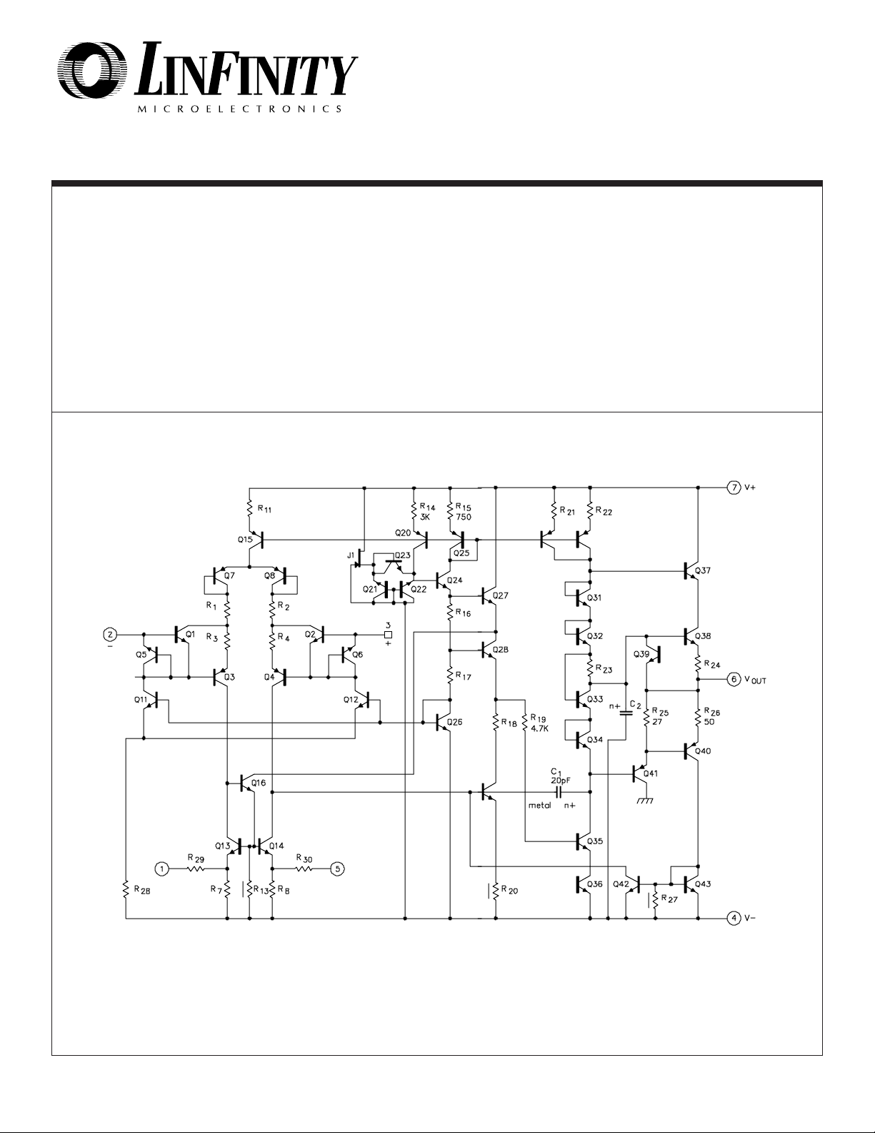
CIRCUIT SCHEMATIC
FEATURES
••
±±
•
±4.0V to
••
±±
••
±±
•
±37V output voltage swing
••
±±
••
±±
•
±24V common-mode voltages
••
±±
••
• Overvoltage protection
••
••
• Output short circuit protection
••
±±
±40V supply voltage range
±±
HIGH RELIABILITY FEATURES-SG143
♦♦
♦ Available to MIL-STD-883 and DESC SMD
♦♦
♦♦
♦ LMI level "S" processing available
♦♦
4/90 Rev 1.1 5/94 LINFINITY Microelectronics Inc.
Copyright 1994 11861 Western Avenue
1 (714) 898-8121
∞ ∞
∞ Garden Grove, CA 92641
∞ ∞
∞∞
∞ FAX: (714) 893-2570
∞∞
Page 2
ABSOLUTE MAXIMUM RATINGS (Note 1)
Supply Voltage
SG143 ............................................................................ ±40V
Input Voltage
SG143 ............................................................................ ±40V
Differential Input Voltage ................................. ±(V
Note 1. Exceeding these ratings could cause damage to the device.
+
+ |V-| - 3) V
THERMAL DATA
T Package:
Thermal ResistanceThermal Resistance-
Y Package:
Thermal ResistanceThermal Resistance-
Junction to Case, θ
Junction to Ambient, θ
Junction to Case, θ
Junction to Ambient, θ
JC
JC
................... 25°C/W
............ 130°C/W
JA
.................. 50°C/W
........... 130°C/W
JA
RECOMMENDED OPERATING CONDITIONS (Note 2)
Supply Voltage
SG143 ........................................................................... ±28V
Note 2. Range over which the device is functional.
SG143
Output Short Circuit Duration............................................ 5 sec
Operating Junction Temperature
Hermetic (T, Y-Package).............................................. 150°C
Storage Temperature Range ............................ -65°C to 150°C
Lead Temperature (Soldering, 10 Seconds) ................... 300°C
Note A. Junction Temperature Calculation: TJ = TA + (PD x θJA).
Note B. The above numbers for θ
thermal resistance of the package in a standard mounting configuration. The θ
guidelines for the thermal performance of the device/pcboard system. All of the above assume no ambient
airflow.
Input Voltage
SG143 ........................................................................... ±28V
Operating Ambient Temperature Range (T
SG143 ............................................................-55°C to 125°C
are maximums for the limiting
JC
numbers are meant to be
JA
)
J
ELECTRICAL CHARACTERISTICS
(Unless otherwise specified, these specifications apply for the operating ambient temperature of 25°C and over the recommended supply voltage
range. Low duty cycle pulse testing techniques are used which maintains junction and case temperatures equal to the ambient temperature.)
Parameter
Input Offset Voltage
Input Offset Current
Input Bias Current
Large Signal Voltage Gain
Common-Mode Rejection
Power Supply Rejection
Input Common Mode Range (Peak)
Unity Gain Bandwidth
Slew Rate
Supply Current
Output Voltage Swing
Short Circuit Current
T
= T
to T
A
MIN
TA = T
MAX
TA = T
T
= T
A
MIN
MIN
.
to T
RL = 100KΩ, V
= T
T
to T
A
MIN
RL =5KΩ
MAX
MAX
MAX
Test Conditions
= ±10V
OUT
SG143
Min. Typ. Max.
2.0
5.0
6.0
1.0
3.0
4.5
7.0
8.0
20
35
180
100
50
80
110
15
100
±24
±25
1.0
2.5
4.0
±22
20
Units
V/mV
V/mV
mV
mV
nA
nA
nA
nA
nA
dB
µV/V
V
MHz
V/µs
mA
V
mA
4/90 Rev 1.1 2/94 LINFINITY Microelectronics Inc.
Copyright 1994 11861 Western Avenue
2 (714) 898-8121
∞ ∞
∞ Garden Grove, CA 92841
∞ ∞
∞∞
∞ FAX: (714) 893-2570
∞∞
Page 3

CHARACTERISTIC CURVES
SG143
FIGURE 1.
POWER BANDWIDTH
FIGURE 3.
OPEN-LOOP FREQUENCY RESPONSE
FIGURE 2.
PEAK OUTPUT VOLTAGE SWING VS. POWER SUPPLY VOLTAGE
FIGURE 4.
OUTPUT SHORT-CIRCUIT CURRENT VS. TEMPERATURE
FIGURE 5.
INPUT CURRENT
4/90 Rev 1.1 2/94 LINFINITY Microelectronics Inc.
Copyright 1994 11861 Western Avenue
3 (714) 898-8121
FIGURE 6.
VOLTAGE GAIN
∞ ∞
∞ Garden Grove, CA 92841
∞ ∞
∞∞
∞ FAX: (714) 893-2570
∞∞
Page 4

CHARACTERISTIC CURVES (continued)
SG143
FIGURE 7.
SUPPLY CURRENT
FIGURE 8.
UNITY GAIN BANDWIDTH
TYPICAL APPLICATIONS
FIGURE 9 - VOLTAGE OFFSET
NULL CIRCUIT
COMMON-MODE INPUT VOLTAGE RANGE
CONNECTION DIAGRAMS & ORDERING INFORMATION (See Notes Below)
Ambient
Temperature Range
Connection Diagram
INVERTING INPUT
8-PIN METAL CAN
T - PACKAGE
Part No.Package
SG143T/883B -55°C to 125°C
SG143T/DESC -55°C to 125°C
SG143T -55°C to 125°C
FIGURE 11 - LOW-DRIFT SAMPLE AND HOLDFIGURE 10 - DIFFERENTIAL AMPLIFIER WITH ±20V
OFFSET ADJUST
NON-INVERTING
INPUT
N.C.
8
5
4
V -
V+
OUTPUT
OFFSET ADJUST
17
26
3
8-PIN CERAMIC DIP
Y- PACKAGE
SG143Y/883B -55°C to 125°C
SG143Y/DESC -55°C to 125°C
SG143Y -55°C to 125°C
OFFSET ADJUST
INVERTING INPUT
NON-INVERTING INPUT
8
1
2
3
4
V-
N.C.
7
V+
6
OUTPUT
5
OFFSET ADJUST
Note 1. Contact factory for JAN and DESC product availablity.
2. All packages are viewed from the top.
4/90 Rev 1.1 2/94 LINFINITY Microelectronics Inc.
Copyright 1994 11861 Western Avenue
4 (714) 898-8121
∞ ∞
∞ Garden Grove, CA 92841
∞ ∞
∞∞
∞ FAX: (714) 893-2570
∞∞
 Loading...