

Datasheet SG137AL, SG137AL-883B, SG137AL-DESC, SG137AT, SG137AT-883B Datasheet (Microsemi Corporation)
...Page 1
SG137A/SG237A/SG337A
SG137/SG237/SG337
1.5 AMP NEGATIVE
ADJUSTABLE REGULATOR
DESCRIPTION
The SG137A family of negative adjustable regulators will deliver up to 1.5A
output current over an output voltage range of -1.2V to -37V. Silicon General
has made significant improvements in these regulators compared to previous
devices, such as better line and load regulation, and a maximum output voltage
error of 1%. The SG137 family uses the same chip design and guarantees
maximum output voltage error of ±2%.
Every effort has been made to make these devices easy to use and difficult to
damage. Internal current and power limiting coupled with true thermal limiting
prevents device damage due to overloads or shorts even if the regulator is not
fastened to a heat sink.
The SG137A/137 family of products are ideal complements to the SG117A/
117 adjustable positive regulators.
BLOCK DIAGRAM
FEATURES
••
• 1 % output voltage tolerance
••
••
• 0.01%/V line regulation
••
••
• 0.5% load regulation
••
••
• 0.02%/W thermal regulation
••
••
• Available in hermetic TO-220
••
HIGH RELIABILITY FEATURES
-SG137A/SG137
♦♦
♦ Available to MIL-STD-883 and DESC SMD
♦♦
♦♦
♦ Scheduled for MIL-M38510 QPL listing
♦♦
♦♦
♦ MIL-M38510/11804BYA - JAN137K
♦♦
♦♦
♦ LMI level "S" processing available
♦♦
2/92 Rev 1.1 2/94 LINFINITY Microelectronics Inc.
Copyright 1994 11861 Western Avenue
1 (714) 898-8121
∞ ∞
∞ Garden Grove, CA 92841
∞ ∞
∞∞
∞ FAX: (714) 893-2570
∞∞
Page 2
ABSOLUTE MAXIMUM RATINGS (Note 1)
Power Dissipation ..........................................
Input to Output Voltage Differential ....................................
Storage Temperature Range ............................
Note 1. Exceeding these ratings could cause damage to the device.
Internally Limited
40V
-65°C to 150°C
THERMAL DATA
K Package:
Thermal ResistanceThermal Resistance-
R Package:
Thermal ResistanceThermal Resistance-
T Package:
Thermal ResistanceThermal Resistance-
IG Package:
Thermal ResistanceThermal Resistance-
L Package:
Thermal ResistanceThermal Resistance-
Junction to Leads, θ
Junction to Ambient, θ
Junction to Leads, θ
Junction to Ambient, θ
Junction to Leads, θ
Junction to Ambient, θ
Junction to Leads, θ
Junction to Ambient, θ
Junction to Leads, θ
Junction to Ambient, θ
................ 3.0°C/W
JC
............... 35°C/W
JA
................ 5.0°C/W
JC
.............. 40°C/W
JA
................. 15°C/W
JC
............ 120°C/W
JA
................ 3.5°C/W
JC
.............. 42°C/W
JA
................. 35°C/W
JC
............ 120°C/W
JA
SG137A/SG137 SERIES
Operating Junction Temperature
Hermetic (K, R, T, L, IG-Packages) ...........................
Lead Temperature (Soldering, 10 Seconds) .............
Note A. Junction Temperature Calculation: TJ = TA + (PD x θJA).
Note B. The above numbers for θ
thermal resistance of the package in a standard mounting configuration. The θ
guidelines for the thermal performance of the device/pcboard system. All of the above assume no ambient
airflow.
are maximums for the limiting
JC
numbers are meant to be
JA
150°C
300°C
RECOMMENDED OPERATING CONDITIONS (Note 2 & 3)
Input Voltage Range .............................. -(V
Note 2. Range over which the device is functional.
Note 3. These ratings are applicable for junction temperatures of less than 135°C.
+ 3.5V) to -36V Operating Junction Temperature Range
OUT
SG137A/SG137 ............................................
SG237A/SG237 ............................................
SG337A/SG337 .............................................
-55°C to 150°C
-25°C to 150°C
0°C to 125°C
ELECTRICAL CHARACTERISTICS
(Unless otherwise specified, these specifications apply over full operating ambient temperatures for SG137A/SG137 with -55°C ≤ TA ≤ 150°C, SG237A/
SG237 with -25°C ≤ TA ≤ 150°C, SG337A/SG337 with 0°C ≤ TA ≤ 125°C, |VIN - V
= 100mA (T and L packages). Although power dissipation is internally limited, these specifications are applicable for power dissipations of 2Ω for the T and
L packages, and 20Ω for the K, R, and IG packages. I
testing techniques are used which maintains junction and case temperatures equal to the ambient temperature.)
is 1.5A for the K, R, and IG packages and 0.5A for the T and L packages. Low duty cycle pulse
MAX
Parameter Test Conditions
Reference Voltage (Note 6)
Line Regulation (Note 4, 6)
I
= 10mA, TA = 25°C
OUT
3V ≤ |V
3V ≤ |VIN - V
IN
- V
| ≤ 40V, 10mA ≤ I
OUT
| ≤ 40V, I
OUT
OUT
≤ I
TA = 25°C
Load Regulation (Note 4)
Thermal Regulation (Note 5)
Ripple Rejection
Adjust Pin Current
Adjust Pin Current Change
(Note 6)
10mA ≤ I
|V
OUT|
|V
OUT|
|V
OUT|
|V
OUT|
= 25°C, 10ms pulse
T
A
V
= -10V, f =120Hz
OUT
C
ADJ
C
ADJ
T
= 25°C
A
3V ≤ |V
10mA ≤ I
≤ I
OUT
MAX
≤ 5V, TA = 25°C
≥ 5V, TA = 25°C
≤ 5V
≥ 5V
= 0, TA = 25°C
= 10µF
- V
OUT
OUT
≤ I
| ≤ 40V
MAX
IN
| = 5.0V, and for I
OUT
≤ I
OUT
MAX
MAX
= 500mA (K, R, and IG power packages) and I
OUT
SG137A/SG237A
Min. Typ. Max.
-1.238
-1.250
-1.262
-1.220
-1.250
-1.280
0.005
0.01
5
0.1
0.5
10
0.2
1.0
0.002
0.02
60
66
70
80
65
100
1.0
0.2
SG137/SG237
Min. Typ. Max.
-1.225
-1.200
25
50
66
5
2
-1.250
-1.250
0.01
15
0.3
20
0.3
0.002
60
77
65
2
0.5
-1.275
-1.300
0.02
25
0.5
50
1.0
0.02
100
5
5
OUT
Units
V
V
%/V
mV
%
mV
%
%/W
dB
dB
µA
µA
µA
2/92 Rev 1.1 2/94 LINFINITY Microelectronics Inc.
Copyright 1994 11861 Western Avenue
2 (714) 898-8121
∞ ∞
∞ Garden Grove, CA 92841
∞ ∞
∞∞
∞ FAX: (714) 893-2570
∞∞
Page 3

ELECTRICAL CHARACTERISTICS (continued)
SG137A/SG137 SERIES
Test ConditionsParameter Units
Minimum Load Current
Current Limit
|VIN - V
|V
|V
K, P, R, IG Packages
IN
IN
- V
- V
OUT
OUT
OUT
| ≤ 40V
| ≤ 10V
| ≤ 15V
T, L, Packages
|V
- V
| ≤ 40V, TJ = 25°C
IN
OUT
K, P, R, IG Packages
T, L, Packages
Temperature Stability
Long Term Stability (Note 5)
RMS Output Noise (% of V
(Note 5)
OUT
= 125°C, 1000 Hours
T
A
T
= 25°C, 10Hz ≤ f ≤ 10 KHz (Note 5)
)
A
Test ConditionsParameter
Reference Voltage
(Note 6)
Line Regulation (Note 4, 6)
Load Regulation (Note 4)
Thermal Regulation (Note 5)
Ripple Rejection
Adjust Pin Current
Adjust Pin Current Change
(Note 6)
Minimum Load Current
Current Limit
I
= 10mA, TA = 25°C
OUT
3V ≤ |V
3V ≤ |VIN - V
TA = 25°C
10mA ≤ I
|V
|V
|V
|V
T
V
C
C
T
3V ≤ |V
10mA ≤ I
|VIN - V
|V
|V
K, P, R, IG-Packages
- V
IN
≤ 5V, TA = 25°C
OUT|
≥ 5V, TA = 25°C
OUT|
≤ 5V
OUT|
≥ 5V
OUT|
= 25°C, 10ms pulse
A
= -10V, f =120Hz
OUT
= 0, TA = 25°C
ADJ
= 10µF
ADJ
= 25°C
A
IN
OUT
- V
IN
OUT
- V
IN
OUT
| ≤ 40V, 10mA ≤ I
OUT
| ≤ 40V, I
OUT
≤ I
OUT
MAX
- V
| ≤ 40V
OUT
≤ I
OUT
MAX
| ≤ 40V
| ≤ 10V
| ≤ 15V
OUT
≤ I
MAX
OUT
≤ I
MAX
T, L-Packages
|V
- V
| ≤ 40V, TJ = 25°C
IN
OUT
K, P, R, IG- Packages
T, L-Packages
Temperature Stability
Long Term Stability (Note 5)
RMS Output Noise (% of V
Note4. Regulation is measured at constant junction temperature, using pulse testing with a low duty cycle. Changes in output vo ltage due to heating
effects are covered under the specification for thermal regulation.
Note 5. These parameters, although guaranteed, are not tested in production.
Note 6. I
for K, R, and IG packages is VIN - V
MAX
and V
- V
IN
(Note 5)
= 40V / 150mA.
OUT
OUT
= 125°C, 1000hr
T
A
T
)
= 25°C, 10Hz ≤ f ≤ 10KHz (Note 5)
A
= 3V / 1.5A and VIN - V
OUT
= 40V / 240mA. For T and L packages I
OUT
SG137A/SG237A
2.5
5.0
1.2
1.5
2.2
3.2
0.5
0.8
1.5
0.24
0.15
0.4
0.25
0.6
0.3
1.0
0.5
1.5
1.0
0.003
SG337A
Min. Typ. Max.
-1.238
-1.250
-1.262
-1.220
-1.250
-1.280
0.005
0.01
5
0.1
0.5
10
0.2
1.0
0.002
0.02
60
66
70
80
65
100
1.0
0.2
2.5
1.2
1.5
2.2
3.5
0.5
0.8
1.5
0.24
0.15
0.5
0.25
0.6
0.3
1.0
0.5
1.5
1.0
0.003
SG137/SG237
Min. Typ. Max.Min. Typ. Max.
3
1.5
0.5
0.24
0.15
Min. Typ. Max.
-1.213
-1.200
25
50
66
5
2
5
3
1.5
0.5
0.15
0.10
is VIN - V
MAX
2.5
1.2
2.2
0.8
0.4
0.25
0.6
0.3
0.003
SG337
-1.250
-1.250
0.01
15
0.3
20
0.3
0.003
60
77
65
2
0.5
2.5
1
2.2
0.8
0.4
0.17
0.6
0.3
0.003
OUT
5.0
3.0
mA
mA
%
1.0
%
%
Units
-1.287
-1.300
50
70
%/V
mV
%
mV
%
%/W
0.04
1.0
1.5
0.04
dB
dB
100
10
µA
µA
5
µA
5
mA
mA
6
%
1.0
%
%
= 3V / 500mA
A
A
A
A
V
V
A
A
A
A
2/92 Rev 1.1 2/94 LINFINITY Microelectronics Inc.
Copyright 1994 11861 Western Avenue
3 (714) 898-8121
∞ ∞
∞ Garden Grove, CA 92841
∞ ∞
∞∞
∞ FAX: (714) 893-2570
∞∞
Page 4

CHARACTERISTIC CURVES
SG137A/SG137 SERIES
FIGURE 1.
INPUT/OUTPUT DIFFERENTIAL
VS. OUTPUT CURRENT
FIGURE 4. *
OUTPUT VOLTAGE DEVIATION
VS. OUTPUT CURRENT
* The SG137A has load regulation compensation which
makes the typical unit read close to zero. This band
represents the typical production spread.
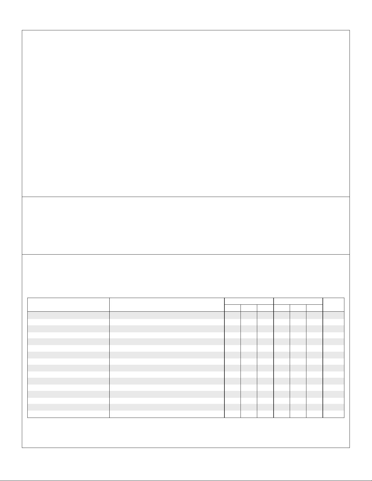
APPLICATION INFORMATION
OUTPUT VOLTAGE
FIGURE 2.
REFERENCE VOLTAGE VS. TEMPERATURE
FIGURE 5.
INPUT/OUTPUT DIFFERENTIAL
VS. OUTPUT CURRENT
FIGURE 3.
CURRENT VS. INPUT/OUTPUT DIFFERENTIAL
FIGURE 6.
ADJUSTMENT CURRENT VS. TEMPERATURE
The output voltage is determined by two external resistors, R
R
(see Figure 7).
2
FIGURE 6
The exact formula for the output voltage is:
R2 + R
V
= V
OUT
REF
( )
2/92 Rev 1.1 2/94 LINFINITY Microelectronics Inc.
Copyright 1994 11861 Western Avenue
1
+ I
(R2)
R
1
ADJ
&
Where: V
1
In most applications, the second term is small enough to be
ignored, typically about 0.5% of V
tions, the exact formula should be used, with I
Solving for R
Smaller values of R
output voltage, but the no-load current drain on the regulator will
be increased. Typical values for R
giving 12.5 mA and 4.2mA no-load current respectively. There
is an additional consideration in selecting R
current specification of the regulator. The operating current of
4 (714) 898-8121
=Reference Voltage, I
REF
yields:
2
V
- V
R
OUT
=
2
V
REF
+ I
R
1
and R2 will reduce the influence of I
1
REF
ADJ
= Adjustment Pin Current.
ADJ
. In more critical applica-
OUT
ADJ
are between 100Ω and 300Ω,
1
the minimum load
1
∞ ∞
∞ Garden Grove, CA 92841
∞ ∞
equal to 65µA.
on the
ADJ
∞∞
∞ FAX: (714) 893-2570
∞∞
Page 5

APPLICATION INFORMATION (continued)
the SG137A flows from input to output. If this current is not
absorbed by the load, the output of the regulator will rise above
the regulated value. The current drawn by R
high enough to absorb the current, but care must be taken in no–
load situations where R
value for the operating current, which must be absorbed, is 5mA
and R2 have high values. The maximum
1
and R2 is normally
1
for the SG137A, If input-output voltage differential is less than
10V, the operating current that must be absorbed drops to 3mA.
The output stability, load regulation, line regulation, thermal
TYPICAL APPLICATIONS
regulation, temperature drift, long term drift, and noise, can be
improved by a factor of 6.6 over the standard regulator configuration. This assumes a zener whose drift and noise is considerably better than the regulator itself. The LM329B has 20PPM/°C
maximum drift and about 10 times lower noise than the regulator.
In the application shown Figure 8, regulators #2 to #N will track
regulator #1 to within ±24mV initially, and to ±60mV over all load,
line, and temperature conditions. If any regulator output is
shorted to ground, all other outputs will drop to -2V. Load
regulation of regulators #2 to #N will be improved by V
compared to a standard regulator, so regulator #1 should be the
one which has the lowest load current.
OUT
/1.25V
SG137A/SG137 SERIES
EXAMPLES:
1. A precision 10V regulator to supply up to 1Amp load current.
a. Select R1 = 100Ω to minimize effect of I
V
- V
OUT
b. Calculate R2 = = = 704W
(V
REF/R1
) + I
REF
ADJ
2. A 15V regulator to run off batteries and supply 50mA.
VIN MAX = 25V
a. To minimize battery drain, select R1 as high as possible
1.25V
R1 = = 417Ω, use 404Ω, 1%
3mA
ADJ
10V - 1.25V
(1.25V/100W) + 65mA
FIGURE 9 - HIGH STABILITY REGULATOR
FIGURE 8 - MULTIPLE TRACKING REGULATORS
FIGURE 11 - DUAL TRACKING SUPPLY ±1.25V to ±20VFIGURE 10 - CURRENT REGULATOR
2/92 Rev 1.1 2/94 LINFINITY Microelectronics Inc.
Copyright 1994 11861 Western Avenue
5 (714) 898-8121
∞ ∞
∞ Garden Grove, CA 92841
∞ ∞
∞∞
∞ FAX: (714) 893-2570
∞∞
Page 6

CONNECTION DIAGRAMS & ORDERING INFORMATION (See Notes Below)
SG137A/SG137 SERIES
3-TERMINAL TO-3
METAL CAN
K-PACKAGE
3-TERMINAL TO-66
METAL CAN
R-PACKAGE
3-PIN TO-39 METAL CAN
T-PACKAGE
Part No.Package
Ambient
Temperature Range
SG137AK/883B -55°C to 125°C
SG137AK/DESC -55°C to 125°C
SG137AK -55°C to 125°C
SG237AK -25°C to 85°C
SG337AK 0°C to 70C
SG137K/883B -55°C to 125°C
JAN137K -55°C to 125°C
SG137K/DESC -55°C to 125°C
SG137K -55°C to 125°C
SG237K -25°C to 85°C
SG337K 0°C to 70°C
SG137AR/883B -55°C to 125°C
SG137AR/DESC -55°C to 125°C
SG137AR -55°C to 125°C
SG237AR -25°C to 85°C
SG337AR 0°C to 70°C
SG137R/883B -55°C to 125°C
SG137R/DESC -55°C to 125°C
SG137R -55°C to 125°C
SG237R -25°C to 85°C
SG337R 0°C to 70°C
SG137AT/883B -55°C to 125°C
SG137AT/DESC -55°C to 125°C
SG137AT -55°C to 125°C
SG237AT -25°C to 85°C
SG337AT 0°C to 70°C
SG137T/883B -55°C to 125°C
SG137T/DESC -55°C to 125°C
SG137T -55°C to 125°C
SG237T -25°C to 85°C
SG337T 0°C to 70°C
Connection Diagram
ADJUSTMENT
V
OUT
ADJUSTMENT
V
OUT
ADJUSTMENT 1
V
OUT
1
2
CASE IS V
IN
1
2
CASE IS V
IN
V
32
IN
3-PIN HERMETIC TO-257
IG-PACKAGE (Isolated)
SG137AIG/883B -55°C to 125°C
SG137AIG/DESC -55°C to 125°C
SG137AIG -55°C to 125°C
SG137IG/883B -55°C to 125°C
SG137IGDESC -55°C to 125°C
V
OUT
V
IN
ADJUST
SG137IG -55°C to 125°C
20-PIN CERAMIC (LCC)
LEADLESS CHIP CARRIER
L- PACKAGE
SG137AL/883B -55°C to 125°C
SG137AL/DESC -55°C to 125°C
SG137AL -55°C to 125°C
SG137L/883B -55°C to 125°C
SG137L/DESC -55°C to 125°C
SG137L -55°C to 125°C
Note 1. Contact factory for JAN and DESC product availability.
2. All parts are viewed from the top.
2/92 Rev 1.1 2/94 LINFINITY Microelectronics Inc.
Copyright 1994 11861 Western Avenue
3. Product is also available in flatpack. Consult factory for price and delivery.
4. Both outputs must be externally connected together at the device terminals.
6 (714) 898-8121
(Note 4)
1. V
2. V
3. N.C.
4. N.C.
5. N.C.
6. N.C.
7. N.C.
8. N.C.
9. N.C.
10. N.C.
321
OUT
OUT
4
5
6
7
8
20 19
911121310
11. V
IN
12. N.C.
13. N.C.
18
14. N.C.
17
15. N.C.
16
16. ADJUST
15
17. N.C.
18. N.C.
14
19. N.C.
20. N.C.
∞ ∞
∞ Garden Grove, CA 92841
∞ ∞
∞∞
∞ FAX: (714) 893-2570
∞∞
 Loading...