

Page 1
Advanced Power MOSFET
SFS9540
FEATURES
n Avalanche Rugged Technology
n Rugged Gate Oxide Technology
n Lower Input Capacitance
n Improved Gate Charge
o
n 175
C Operating Temperature
n Extended Safe Operating Area
n Lower Leakage Current : 10 µA(Max.) @ V
n Low R
: 0.161 Ω (Typ.)
DS(ON)
Absolute Maximum Ratings
Characteristic Value UnitsSymbol
Drain-to-Source Voltage
Continuous Drain Current (T
Continuous Drain Current (T
=25oC)
C
=100oC)
C
Drain Current-Pulsed
Gate-to-Source Voltage
Single Pulsed Avalanche Energy
Avalanche Current
Repetitive Avalanche Energy
Peak Diode Recovery dv/dt
Total Power Dissipation (T
=25oC)
C
Linear Derating Factor
Operating Junction and
Storage Temperature Range
Maximum Lead Temp. for Soldering
Purposes, from case for 5-seconds
1/8”
T
V
DSS
I
I
DM
V
E
I
AR
E
dv/dt
P
, T
J
T
D
GS
AS
AR
D
STG
L
= -100V
DS
O
O
O
O
O
BV
R
DS(on)
DSS
= -100 V
= 0.2
Ω
ID= -10.7 A
TO-220F
1
2
3
1.Gate 2. Drain 3. Source
-100
-10.7
-8.1
1
-43
±30
2
1
1
3
534
-10.7
5.3
-6.5
53
0.35
- 55 to +175
300
V
A
A
V
mJ
A
mJ
V/ns
W
W/
o
o
C
C
Thermal Resistance
Symbol Typ.
R
θJC
R
θJA
Characteristic Max.
Junction-to-Case
Junction-to-Ambient
Units
--
--
2.83
62.5
o
C/W
Rev. C
Page 2
SFS9540
P-CHANNEL
POWER MOSFET
Electrical Characteristics
CharacteristicSymbol
BV
∆BV/∆T
V
GS(th)
I
GSS
I
DSS
R
DS(on)
g
C
C
C
t
d(on)
t
d(off)
Q
Q
Q
Drain-Source Breakdown Voltage
DSS
Breakdown Voltage Temp. Coeff.
J
Gate Threshold Voltage
Gate-Source Leakage , Forward
Gate-Source Leakage , Reverse
Drain-to-Source Leakage Current
Static Drain-Source
On-State Resistance
Forward Transconductance
fs
Input Capacitance
iss
Output Capacitance
oss
Reverse Transfer Capacitance
rss
Turn-On Delay Time
t
Rise Time
r
Turn-Off Delay Time
t
Fall Time
f
Total Gate Charge
g
Gate-Source Charge
gs
Gate-Drain("Miller") Charge
gd
(TC=25oC unless otherwise specified)
Max. UnitsTyp.Min. Test Condition
V
-100
--
-2.0
--
--
--
--
--
--
--
--
--
--
--
--
--
--
--
--
--
-0.11
--
--
--
--
--
--
8.5
1180
240
83
14
22
45
26
43
7.4
17.8
--
--
-4.0
-100
100
-10
-100
0.2
--
1535
360
125
40
55
100
60
54
--
--
V
V/oC
V
nA
µA
Ω
S
pF
ns
nC
=0V,ID=-250µA
GS
I
=-250µA See Fig 7
D
V
=-5V,ID=-250µA
DS
V
=-20V
GS
V
=20V
GS
VDS=-100V
V
=-80V,TC=150oC
DS
=-10V,ID=-5.4A
V
GS
=-40V,ID=-5.4A
V
DS
VGS=0V,VDS=-25V,f =1MHz
VDD=-50V,ID=-17A,
R
=12
G
V
=-80V,VGS=-10V,
DS
I
=-17A
D
See Fig 6 & Fig 12
See Fig 5
Ω
See Fig 13
O
O
4
O
4
O
4
5
O
4
5
O
Source-Drain Diode Ratings and Characteristics
CharacteristicSymbol Max. UnitsTyp.Min. Test Condition
I
I
SM
V
t
Q
Notes ;
Repetitive Rating : Pulse Wi dth Lim i ted by Maximum Junction Temperature
1
O
2
L=7.0mH, I
O
3
I
O
4
Pulse Test : Pulse Width = 250µs, Duty Cycle 2%
O
5
Essentially Independent of Operating Temperature
O
Continuous Source Current
S
Pulsed-Source Current
Diode Forward Voltage
SD
Reverse Recovery Time
rr
Reverse Recovery Charge
rr
=-10.7A, VDD=-25V, RG=27Ω*, Starting TJ =25oC
AS
_
<
-17A, di/dt 450A/µs, VDDBV
SD
_
<
_
<
DSS
--
1
--
O
4
--
O
--
--
, Starting TJ =25oC
_
<
--
--
--
135
0.7
-10.7
-43
-4.0
--
--
A
V
ns
µC
Integral reverse pn-diode
in the MOSFET
T
=25oC,IS=-10.7A,VGS=0V
J
T
=25oC,IF=-17A
J
di
/dt=100A/µs
F
O
4
Page 3
P-CHANNEL
POWER MOSFET
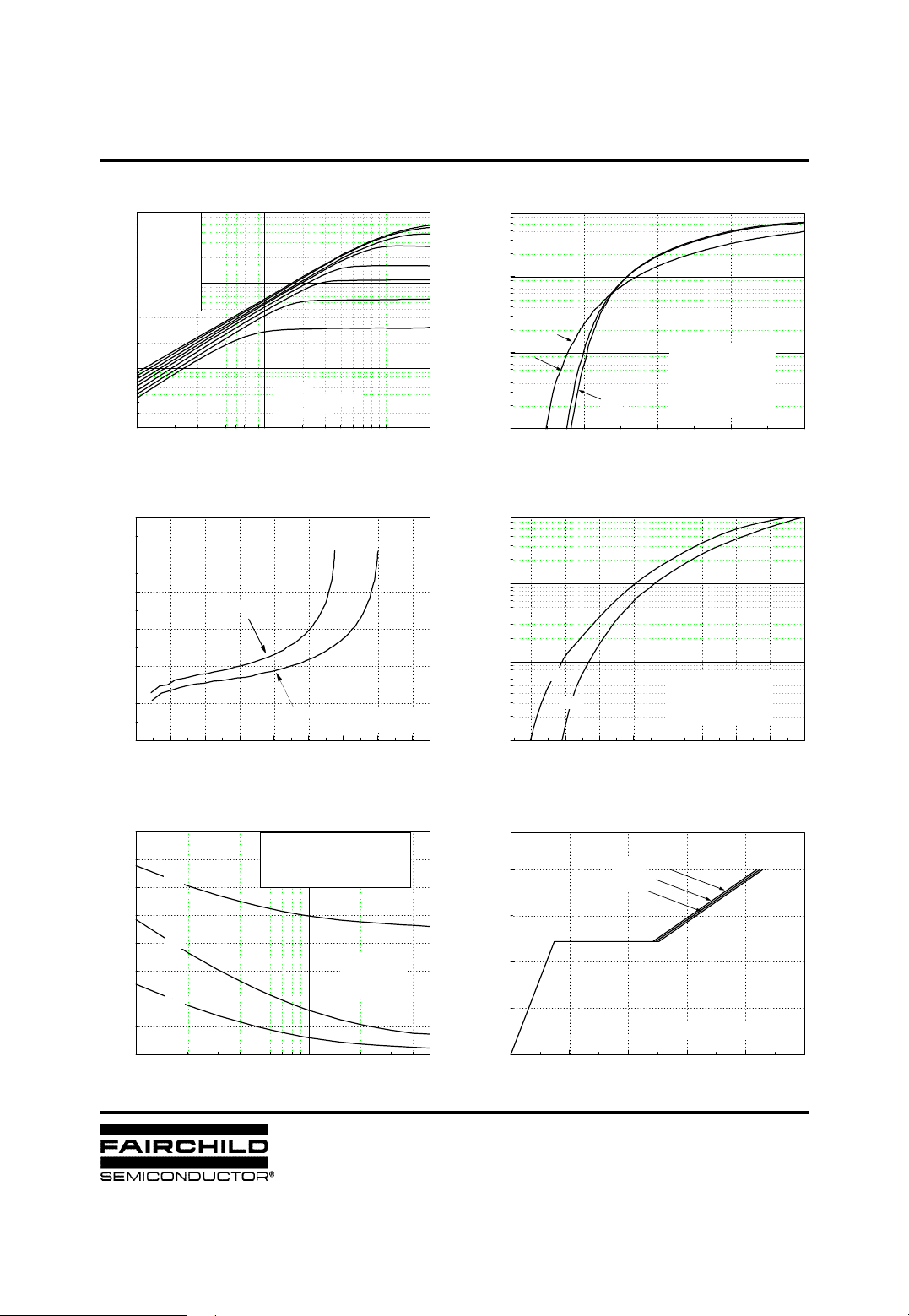
Fig 1. Output Characteristics Fig 2. Transfer Characteristics
V
GS
Top : - 1 5 V
- 10 V
- 8.0 V
- 7.0 V
- 6.0 V
1
- 5.5 V
10
- 5.0 V
Bott om : - 4.5 V
0
10
, Drain Current [A]
D
-I
-1
10
-VDS , Drain-Source Voltage [V]
@ Notes :
1. 250 µs Pulse Test
2. TC = 25 oC
0
10
SFS9540
1
10
175 oC
25 oC
0
10
, Drain Current [A ]
D
-I
-1
1
10
10
246810
- 55 oC
-VGS , Gate-Source Vo ltage [V]
@ Notes :
1. V
2. V
3. 250
= 0 V
GS
= -40 V
DS
s Pulse Test
µ
0.6
0.5
]
Ω
0.4
, [
DS(on)
R
0.3
VGS = -10 V
0.2
Drain-Source On-Resistance
0.1
0.0
0 8 16 24 32 40 48 56 64
VGS = -20 V
-ID , Drain Current [A ]
2000
C
1500
1000
Capacitance [pF]
500
iss
C
oss
C
rss
0
0
10
C
= Cgs+ Cgd ( Cds= shorted )
iss
= Cds+ C
C
oss
gd
C
= C
rss
gd
1
10
-VDS , Drain-Source Voltage [V]
@ Note : TJ = 25 oC
@ Notes :
1. V
= 0 V
GS
2. f = 1 MHz
Fig 4. Source-Drain Diode Forward VoltageFig 3. On-Resistance vs. Drain Current
1
10
0
10
175 oC
, Reverse Drain C urrent [A]
DR
-I
-1
10
25 oC
0.5 1.0 1.5 2.0 2.5 3.0 3.5 4.0 4.5
@ Notes :
1. V
2. 250
= 0 V
GS
s Pulse Test
µ
-VSD , Source-Drain Voltage [V]
Fig 6. Gate Charge vs. Gate-Source VoltageFig 5. Capacitance vs. Drain-Source Voltage
10
5
, Gate-Source Vo ltage [V]
GS
-V
0
0 1020304050
VDS = -20 V
VDS = -50 V
VDS = -80 V
@ Notes : ID =-17 A
QG , Total Gate Char ge [nC]
Page 4

SFS9540
Fig 7. Breakdown Voltage vs. Temperature Fig 8. On-Resistance vs. Temperature
1.2
2.5
POWER MOSFET
P-CHANNEL
1.1
1.0
, (Normalized)
DSS
-BV
0.9
Drain-Source Breakdown Voltage
0.8
-75 -50 -25 0 25 50 75 100 125 150 175 200
@ Notes :
1. V
2. I
TJ , Junction Temperature [oC]
Operation in This Area
is Limited by R
2
10
DS(on)
0.1 ms
, Drain Current [A]
D
-I
1
10
@ No t e s :
@ No t e s :
@ No t e s :@ No t e s :
1. TC = 25 oC
0
10
-1
10
0
10
= 175 oC
2. T
J
3. Single Pulse
1
10
1 ms
10 ms
DC
-VDS , Drain-Source Voltag e [V]
= 0 V
GS
= -250 µA
D
10
2.0
1.5
1.0
, (Normalized)
DS(on)
R
0.5
Drain-Source On-Resistance
0.0
-75 -50 -25 0 25 50 75 100 125 150 175 200
@ Notes :
1. V
2. I
= -10 V
GS
= -8.5 A
D
TJ , Junction Temperature [oC]
Fig 10. Max. Drain Current vs. Case TemperatureFig 9. Max. Safe Operating Area
12
9
6
, Drain Current [A ]
D
3
-I
2
0
25 50 75 100 125 150 175
Tc , Case Temperature [oC]
Fig 11. Thermal Response
D=0.5
0
10
0.2
0.1
0.05
-1
0.02
10
0.01
(t) , Thermal Response
JC
θ
Z
-5
10
single pulse
-4
10
-3
10
10
@ Notes :
1. Z
2. Duty Factor, D=t1/t
3. TJM-TC=PDM*Z
-2
(t)=2.83 oC/W Max.
JC
θ
P
DM
.
t
-1
10
2
(t)
JC
θ
1.
t
2.
0
10
1
10
t1 , Square Wave Pulse Durati on [sec]
Page 5

P-CHANNEL
POWER MOSFET
SFS9540
Fig 12. Gate Charge Test Circuit & Waveform
12V
-10V
“ Current Regulator
200nF
-3mA
V
R
G
”
50KΩ
300nF
V
GS
R
1
Current Sampling (IG)
Resistor
Fig 13. Resistive Switching Test Circuit & Waveforms
V
out
in
DUT
Same Type
as DUT
DUT
R
2
Current Sampling (ID)
Resistor
R
L
V
DD
( 0.5 rated V
V
GS
Q
-10V
V
DS
Q
gs
g
Q
gd
Charge
t
on
t
d(on)tr
)
DS
V
in
10%
90%
V
out
t
off
t
f
t
d(off)
Vary tpto obtain
required peak I
-10V
Fig 14. Unclamped Inductive Switching Test Circuit & Waveforms
BV
L
V
DS
D
R
G
L
I
D
V
DD
C
V
DD
E
=LL I
AS
----
1
2
2
AS
t
p
I
(t)
D
DSS
-------------------BV
DSS
-- V
DD
Time
V
(t)
DS
DUT
I
AS
t
p
BV
DSS
Page 6

SFS9540
Fig 15. Peak Diode Recovery dv/dt Test Circuit & Waveforms
+
V
DS
DUT
--
I
S
L
P-CHANNEL
POWER MOSFET
V
GS
( Driver )
I
S
( DUT )
V
DS
( DUT )
V
GS
V
GS
Driver
R
G
D =
IFM, Body Diode Forward Current
Comp limen t of DUT
Gate Pulse Width
-------------------------Gate Pulse Period
Body Diode
Forward Voltage Drop
(N-Channel)
• dv/dt controlled by “RG”
•I
controlled by Duty Factor “D”
S
Body Diode Reverse Current
I
RM
V
f
di/dt
V
DD
10V
V
DD
Body Diode Recovery dv/dt
Page 7

TRADEMARKS
The following are registered and unregistered trademarks Fairchild Semiconductor owns or is authorized to use and is
not intended to be an exhaustive list of all such trademarks.
ACEx
ActiveArray
Bottomless
CoolFET
CROSSVOL T
DOME
EcoSPARK
E2CMOS
EnSigna
TM
TM
FACT
FACT Quiet Series
â
FAST
FASTr
FRFET
GlobalOptoisolator
GTO
HiSeC
I2C
Across the board. Around the world.
The Power Franchise
Programmable Active Droop
ImpliedDisconnect
ISOPLANAR
LittleFET
MicroFET
MicroPak
MICROWIRE
MSX
MSXPro
OCX
OCXPro
OPTOLOGIC
â
OPTOPLANAR
PACMAN
POP
Power247
PowerTrench
â
QFET
QS
QT Optoelectronics
Quiet Series
RapidConfigure
RapidConnect
SILENT SWITCHER
SMART START
SPM
Stealth
SuperSOT-3
SuperSOT-6
SuperSOT-8
SyncFET
TinyLogic
TruTranslation
UHC
UltraFET
â
VCX
â
DISCLAIMER
FAIRCHILD SEMICONDUCTOR RESERVES THE RIGHT TO MAKE CHANGES WITHOUT FURTHER
NOTICE TO ANY PRODUCTS HEREIN TO IMPROVE RELIABILITY, FUNCTION OR DESIGN. FAIRCHILD
DOES NOT ASSUME ANY LIABILITY ARISING OUT OF THE APPLICATION OR USE OF ANY PRODUCT
OR CIRCUIT DESCRIBED HEREIN; NEITHER DOES IT CONVEY ANY LICENSE UNDER ITS PATENT
RIGHTS, NOR THE RIGHTS OF OTHERS.
LIFE SUPPORT POLICY
FAIRCHILDS PRODUCTS ARE NOT AUTHORIZED FOR USE AS CRITICAL COMPONENTS IN LIFE SUPPORT
DEVICES OR SYSTEMS WITHOUT THE EXPRESS WRITTEN APPROVAL OF FAIRCHILD SEMICONDUCTOR CORPORATION.
As used herein:
1. Life support devices or systems are devices or
systems which, (a) are intended for surgical implant into
the body, or (b) support or sustain life, or (c) whose
failure to perform when properly used in accordance
with instructions for use provided in the labeling, can be
reasonably expected to result in significant injury to the
user.
PRODUCT STATUS DEFINITIONS
Definition of Terms
Datasheet Identification Product Status Definition
Advance Information
Preliminary
No Identification Needed
Formative or
In Design
First Production
Full Production
2. A critical component is any component of a life
support device or system whose failure to perform can
be reasonably expected to cause the failure of the life
support device or system, or to affect its safety or
effectiveness.
This datasheet contains the design specifications for
product development. Specifications may change in
any manner without notice.
This datasheet contains preliminary data, and
supplementary data will be published at a later date.
Fairchild Semiconductor reserves the right to make
changes at any time without notice in order to improve
design.
This datasheet contains final specifications. Fairchild
Semiconductor reserves the right to make changes at
any time without notice in order to improve design.
Obsolete
Not In Production
This datasheet contains specifications on a product
that has been discontinued by Fairchild semiconductor.
The datasheet is printed for reference information only.
Rev. I1
 Loading...