

Page 1

r
)
)
.
.
SFH636
HIGH SPEED 5.3 kV OPTOCOUPLER
Preliminary Data Sheet
FEATURES
• High Speed Optocoupler without Base
Connection
• GaAlAs Emitter
• Integrated Detector with Photodiode and
Transistor
• High Data Transmission Rate: 1 MBit/s
• TTL Compatible
• Open Collector Output
• CTR at I
T
A
=16 mA, V
F
=25 ° C: ≥ 19%
=0.4 V , V
O
CC
=4.5 V ,
• Good CTR Linearity Relative to Forward Current
• Field Effect Stable by TRIOS
(TRansparent IOn Shield)
• Low Coupling Capacitance
• dV/dt: typ. 10 kV/ µ s
• Isolation T est V oltage: 5300 VA C
RMS
• VDE 0884 Available with Option 1
• UL Approval, File #E52744
APPLICATIONS
• IGBT Drivers
• Data Communications
• Programmable Controllers
DESCRIPTION
The SFH636 is an optocoupler with a GaAlAs infrared
emitting diode, optically coupled to an integrated photodetector consisting of a photodiode and a high
speed transistor in a DIP-6 plastic package. The
device is functionally similar to 6N136 except there is
no base connection, and the electrical foot print is
different. Noise and dv/dt performance is enhanced
by not bringing out the base connection.
Signals can be transmitted between two electrically
separated circuits up to frequencies of 2 MHz. The
potential difference between the circuits to be coupled should not exceed the maximum permissible
reference voltages.
Package Dimensions in Inches (mm)
Pin One ID.
12
5
6
Cathode
.130 (3.30)
.150 (3.81)
.020 (.051) min.
.031 (0.80)
.035 (0.90)
.100 (2.54) typ.
Anode
NC
1
2
3
18° typ.
.300 (7.62)
typ.
.010 (.25)
.014 (.35)
.300 (7.62)
.347 (8.82)
V
6
CC
5
Emitter
Collecto
4
.110 (2.79
.150 (3.81
248 (6.30)
256 (6.50)
.039
(1.00)
min.
4°
typ.
.018 (0.45)
.022 (0.55)
3
4
.335 (8.50)
.343 (8.70)
Absolute Maximum Ratings
Emitter (GaAlAs)
Reverse Voltage.............................................................................3 V
DC Forward Current..................................................................25 mA
Surge Forward Current..................................................................1 A
tp ≤
1 µ s, 300 pulses/sec.
Total Power Dissipation............................................................45 mW
Detector (Si Photodiode + Transistor)
Supply Voltage.................................................................–0.5 to 30 V
Output Voltage................................................................. –0.5 to 20 V
Output Current............................................................................8 mA
Total Power Dissipation..........................................................100 mW
Package Insulation
Isolation Test Voltage
between emitter and detector
(refer to climate DIN 40046, part 2, Nov. 74) ...........5300 VAC
RMS
Creepage........................................................................... 7 mm min.
Clearance .......................................................................... 7 mm min.
Comparative Tracking Index
per DIN IEC 112/VDE0303, part 1 ............................................ 175
Isolation Resistance
V
=500 V, T
IO
V
=500 V, T
IO
=25 ° C........................................................... ≥ 10
A
=100 ° C......................................................... ≥ 10
A
12
Ω
11
Ω
Storage Temperature Range........................................–55 to +150 ° C
Ambient Temperature Range.......................................–55 to +100 °
Junction Temperature...............................................................100 °
Soldering Temperature (t=10 sec. max.).................................260 °
Dip soldering: distance to seating plane ≥
1.5 mm
C
C
C
5–260
Page 2

t
=0 °
Characteristics (T
to 70 ° C, unless otherwise specified,typical values T
A
=25 ° C)
A
Description Symbol Min. Typ. Max. Unit
Emitter (IR GaAlAs)
Forward Voltage, I
Reverse Current, V
Capacitance, V
Thermal Resistance R
=16 mA V
F
=3 V I
R
=0 V, f=1 MHz C
R
R
F
0
thJA
1.5 1.8 V
0.5 10
125 pF
700
Detector (Si Photodiode + Transistor)
Supply Current, Logic High
I
=0, V
I
F
=0, V
F
(open), V
O
(open), V
O
=15 V, T
CC
=15 V
CC
=25 ° C
A
Output Current, Output High
I
=0, V
(open), V
F
O
I
=0, V
(open), V
F
O
I
=0, V
(open), V
F
O
Capacitance, V
=5.5 V, T
CC
=15 V, T
CC
=15 V
CC
=5 V, f=1 MHz C
CE
=25 ° C
A
=25 ° C
A
Thermal Resistance R
I
I
CCH
OH
CE
thJA
0.01 1
2
.003
.01
—
0.5
1
50
3pF
300
Package
Coupling Capacitance C
Coupling Transfer Ratio
I
=16 mA, V
F
I
=16 mA, V
F
=0.4 V, V
O
=0.5 V, V
O
=4.5 V, T
CC
=4.5 V
CC
=25 ° C
A
Collector Emitter Saturation Voltage
I
=16 mA, I
F
=2.4 mA, V
O
=4.5 V, T
CC
=25 ° C
A
Supply Current, Logic Low
I
=16 mA, V
F
open, V
O
CC
=15 V
I
V
I
C
/I
C
OL
CCL
F
19
15
0.6 pF
30
—
0.1 0.4 V
80
µ A
° K/W
µ A
µ A
° K/W
%
µ A
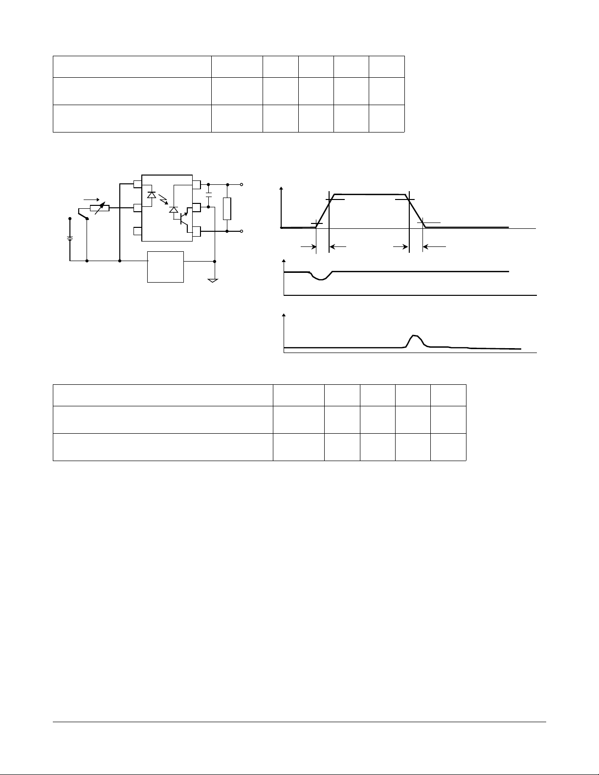
Figure 1. Test set-up Figure 2. Switching time measurement
Vcc
Vo
Vout
0
I
0
t
PHL
F
16 mA
100 Ω
Pulse generator
Zo=50 Ω
tr,tf=5 ns
Duty cycle=10%
Period =100 µs
I
F
1
2
3
6
5
4
C
L
C=100 nF
=15pF
R
L
1.5V
t
PLH
5V
t
SFH636
5–261
Page 3
Description Symbol Min. Typ. Max. Unit
t
t
t
Propagation Delay Time (High–Low)
I
=16 mA, V
F
=5 V, R
CC
=1.9 k Ω , T
L
=25 ° C
A
Propagation Delay Time (Low–High)
I
=16 mA, V
F
=5 V, R
CC
=1.9 k Ω , T
L
=25 ° C
A
t
t
PHL
PLH
0.3 0.8
0.3 0.8
µ s
µ s
Figure 3. Common mode transient test Figure 4. Measurement waveform of CMR
1
I
F
B
V
FF
A
2
3
Pulse
generator
common
mode
6
5
R
L
4
C=100 nF
Vcc
Vo
V
CM
90%
10%
10%
0
t
Vo
R
5V
0
Vo
V
OL
0
90%
t
F
A: I
=0 mA
F
B: IF=16 mA
Description Symbol Min. Typ. Max. Unit
Common Mode Transient Immunity (High)
I
=0, V
F
=1500 V
CM
P-P
, R
=1.9 k Ω , V
L
CC
=5 V, T
Common Mode Transient Immunity (Low)
IF=16 mA, VCM=1500 V
, RL=1.9 kΩ, VCC=5 V, TA=25°C
P-P
=25 ° C
A
CM
CM
H
L
10 kV/µs
10 kV/µs
SFH636
5–262
 Loading...