

Page 1
≤ 70 °
≤ 70 °
Ω
≥
Ω
SFH6135 / SFH6136
HIGH-SPEED 5.3 kV TRIOS“
OPTOCOUPLER
FEATURES
• Isolation Test Voltage: 5300 V
RMS
• TTL Compatible
• High Bit Rates: 1.0 Mbit/s
• High CoMmon-mode Interference Immunity
• Bandwidth 2.0 MHz
• Open-collector Output
• External Base Wiring Possible
• Field-effect Stable by TRIOS
(TRansparent IOn Shield)
• Underwriters Lab File #52744
V
• VDE 0884 Available with Option 1
DE
Description
The SFH6135 and SFH6136 optocouplers feature
a high signal transmission rate and a high isolation resistance. They have a GaAIAs infrared
emitting diode, optically coupled with an integrated photodetector which consists of a photodiode and a high-speed transistor in a DIP-8
plastic package.
Signals can be transmitted between two electrically separated circuits up to frequencies of 2.0
MHz. The potential difference between the circuits to be coupled is not allowed to exceed the
maximum permissible reference voltages.
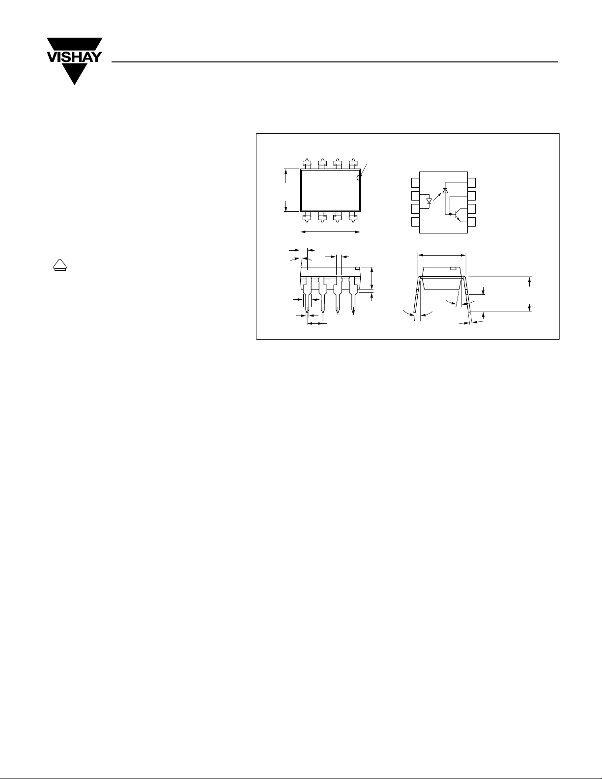
Dimensions in inches (mm)
pin one ID
.255 (6.48)
.268 (6.81)
.030 (0.76)
.045 (1.14)
4° typ.
.050 (1.27)
.018 (.46)
.022 (.56)
4
3
5
6
.379 (9.63)
.390 (9.91)
1
2
78
.031 (0.79)
.020 (.51 )
.035 (.89 )
.100 (2.54) typ.
NC
Anode
Cathode
NC
.130 (3.30)
.150 (3.81)
1
2
3
4
.300 (7.62)
typ.
3°–9°
.008 (.20)
.012 (.30)
10°
Cathode
8
(VCC)
Base
7
(V
)
B
Collector
6
(V
)
O
Emitter
5
(GND)
.110 (2.79)
.130 (3.30)
.230(5.84)
.250(6.35)
Maximum Ratings
Emitter
Reverse Voltage........................................................................................ 3.0 V
Forward Current ...................................................................................... 25 mA
Peak Forward Current (t =1.0 ms, duty cycle 50%)................................ 50 mA
Maximum Surge Forward Current (t ≤ 1.0 µ s, 300 pulses/s) .....................1.0 A
Thermal Resistance .............................................................................700 K/W
Total Power Dissipation ( T
C) ......................................................... 45 mW
A
Detector
Supply Voltage............................................................................... –0.5 to 30 V
Output Voltage ............................................................................... –0.5 to 25 V
Emitter-base Voltage ................................................................................. 5.0 V
Output Current .......................................................................................8.0 mA
Maximum Output Current........................................................................ 16 mA
Base Current .......................................................................................... 5.0 mA
Thermal Resistance .............................................................................300 K/W
Total Power Dissipation ( T
C) ....................................................... 100 mW
A
Package
Isolation Test Voltage ...................................................................... 5300 V
RMS
Pollution Degree (DIN VDE 0110) ................................................................... 2
Creepage ........................................................................................... ≥ 7.0 mm
Clearance........................................................................................... ≥ 7.0 mm
Comparative Tracking Index per DIN IEC112/VDE 0303 part 1 ................. 175
Isolation Resistance
V
=500 V, T
IO
V
=500 V, T
IO
=25 ° C .......................................................................... ≥ 10
A
=100 ° C ........................................................................ ≥ 10
A
12
11
Storage Temperature Range................................................. –55 ° C to +125 ° C
Ambient Temperature Range ................................................ –55 ° C to +100 ° C
Soldering Temperature (max. ≤ 10 s. dip soldering
0.5 mm distance from case bottom).................................................. 260 ° C
Document Number: 83668 www.vishay.com
Revision 17-August-01
2–271
Page 2
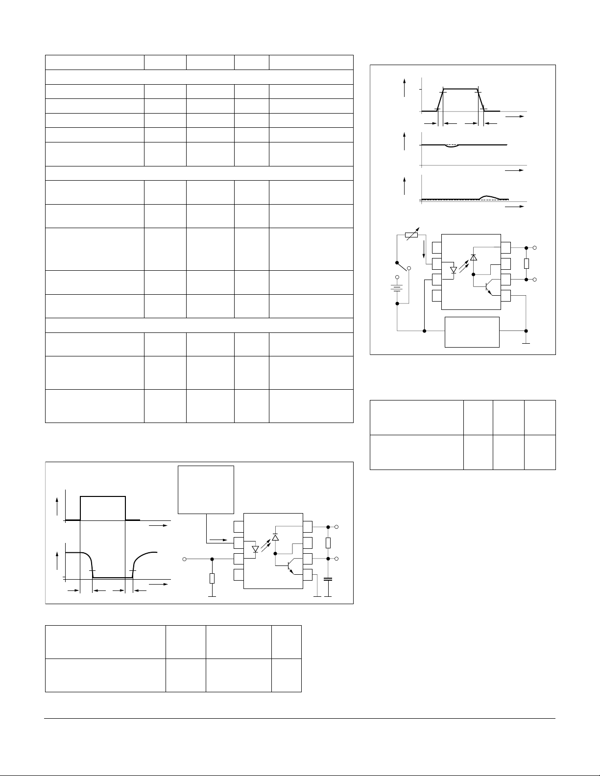
1
2
3
4
8
7
6
5
V
CM
V
O
V
O
10 V
5 V
0 V
V
OL
90%
10% 90%
10%
t
r
t
f
t
t
t
A: I
F
=0 mA
B: I
F
=16 mA
B
V
CC
I
F
+V
CM
V
O
R
L
5 V
A
Pulse generator
Z
O
=50 Ω
t
r
,
tf=8 ns
BR
∆
/ ∆
C
µ A
=
=
Table 4. Characteristics ( T
=25 ° C, unless otherwise specified)
A
Symbol Unit Condition
Figure 2. Common-mode interference
immunity
Emitter
Forward Voltage
Breakdown Voltage
Reverse Current
Capacitance
Temperature Coefficient
of Forward Voltage
V
F
V
I
R
C
O
V
F
1.6 (
≤
3.0 V
≥
0.5 (
≤
125 pF
T
1.7 mV/
A
1.9) V
10) µ A
I
=16 mA
F
I
=10 µ A
R
V
=3.0 V
R
V
=0 V, f=1.0 MHz
R
°
I
=16 mA
F
Detector
Supply Current,
Logic Low I
Supply Current,
Logic High I
Output Voltage,
Output Low
SFH6135
SFH6136
Output Current,
Output High
Output Current,
Output High
CCL
CCH
V
OL
V
OL
I
OH
I
OH
150
0.01 (
0.1 (
0.1 (
3.0 (
0.01 (
≤
1.0) µ A
0.4)
≤
≤
0.4)VV
≤
500) nA
≤
1.0) µ A
I
=16 mA, V
F
=15 V
V
CC
I
=0 mA, V
F
V
=15 V
CC
I
=16 mA,
F
V
=4.5 V
CC
I
=1.1 mA
O
I
=2.4 mA
O
I
=0 mA,
F
V
V
O
CC
I
=0 mA
F
V
V
O
CC
O
open,
O
=5.5 V
=15 V
open,
Package
Coupling CapacitanceInput-output
Current Transfer Ratio
SFH6135
SFH6136
Current Transfer Ratio
SFH6135
SFH6136
SWITCHING TIMES
Figure 1. Schematic
I
F
V
O
V
OL
Delay Time ( I
t
PHL
=16 mA, V
F
High - Low
SFH6135 (R
SFH6136 (R
Low - High
SFH6135 (RL=4.1 kΩ)
SFH6136 (RL=1.9 kΩ)
=4.1 kΩ)
L
=1.9 kΩ)
L
C
IO
CTR
CTR
CTR
CTR
5 V
1.5 V
t
PLH
=5.0 V, T
CC
0.6 pF f=1.0 MHz
7.0)
≥
16 (
≥
19)%%
35 (
1
I
F
2
3
4
100 Ω
0.3 (≤1.5)
≤0.8)
0.2 (
0.3 (≤1.5)
0.2 (≤0.8)
%
%
Pulse generator
Z
O
t
tf=5 ns
,
r
duty cycle 10%
t≤100 µs
t
I
F
t
A
t
PHL
t
PHL
t
PLH
t
PLH
5.0
≥
≥15
=50 Ω
Monitor
=25°C)
I
=16 mA, V
F
V
=4.5 V, T
CC
I
=16 mA, VO=0.5 V,
F
=4.5 V
V
CC
=0.4 V,
O
=25
A
8
7
6
5
µs
µs
µs
µs
R
L
C
15 pF
5 V
V
L
Table 1. Common Mode Interference
C
°
Immunity
V
CM
=10 V
, VCC=5.0 V, TA=25°C
P–P
High (IF=0 mA)
=16 mA)
F
=4.1 kΩ)
L
=1.9 kΩ)
L
=4.1 kΩ)
L
=1.9 kΩ)
L
SFH6135 (R
SFH6136 (R
Low (I
SFH6135 (R
SFH6136 (R
O
CM
CM
CM
CM
1000
H
1000
H
1000
L
1000
L
V/µs
µs
V/
V/µs
µs
V/
Document Number: 83668 www.vishay.com
Revision 17-August-01
2–272
Page 3

Figure 3. LED forward current vs. forward voltage
20
15
10
5
- LED Current in mA
F
I
0
75°C
VF - LED forward Voltage
25°C
0°C
Figure 6. Output Current vs. Output Voltage
(T
=25°C, VCC=5.0 V)
A
25
IF=40mA
20
15
10
5
Output Current, Io(mA)
1.71.61.51.41.3
0
0 5 10 15 20 25
Output Voltage, Vo(V)
IF=35mA
IF=30mA
IF=25mA
IF=20mA
IF=15mA
IF=10mA
IF=5mA
Figure 4. Permissible forward LED current vs. temperature
30
20
10
LED Current in ma
F
I
0
100806040200
Ambient Temperature in °C
Figure 5. Permissible power dissipation vs. temperature
120
100
80
60
40
Total Power in mW
20
0
Detector
Emitter
100806040200
Ambient Temperature in °C
Figure 7. Output Current vs. Temperature
@ V
=0.4 V, VCC=5.0
O
8
7
IF = 20mA
IF = 16mA
6
5
4
IF = 10mA
IF = 2mA
3
2
Output Current, Io(mA)
1
IF = 1mA
0
-60 -40 -20 0 20 40 60 80 100
Temperature, Ta(°C)
Figure 8. Propagation Delay vs. Temperature-SFH6136
@ V
=5.0 V, IF=16 mA, RL=1.9 kΩ
CC
900
800
700
600
500
400
300
200
100
tp - Propagation Delay Time - ns
0
-60 -40 -20 0 20 40 60 80 100
Temperature, Ta(°C)
TpLH @ 3V
TpLH @ 1.5V
TpHL @ 1.5V
TpHL @ 3V
Document Number: 83668 www.vishay.com
Revision 17-August-01
2–273
Page 4

Figure 9. Propagation Delay vs. Temperature-SFH6135
@ V
=5.0 V, IF=16 mA, RL=4.1 kΩ
CC
1400
1200
1000
800
600
TpLH
400
200
tp - Propagation Delay Time - ns
0
TpHL
-60 -40 -20 0 20 40 60 80 100
Temperature, Ta(°C)
Figure 10. Logic High Output Current vs. Temperature
100
10
1
VCC=VO=15 V
VCC=VO=5 V
0.1
0.01
- Collector Current, IC (nA)
OH
I
0.001
-60 -40 -20 0 20 40 60 80 100
Temperature, T
(°C)
A
Figure 11. Small Signal Current Transfer Ratio vs. Quiescent
Input Current (V
0.6
0.5
0.4
0.3
0.2
Transfer Ratio
/ Small Signal Current
O
0.1
/∆i
F
∆i
0
0 5 10 15 20 25
=5.0 V, RL=100 Ω)
CC
IF / mA
Document Number: 83668 www.vishay.com
Revision 17-August-01
2–274
 Loading...