

Page 1
Ostar Observation
Lead (Pb) Free Product - RoHS Compliant
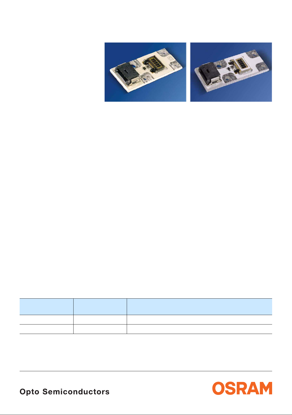
SFH 4730, SFH 4740
SFH 4730
SFH 4730
• Schwarzer Rahmen zur Streulichtminimierung
•3 W optische Leistung
SFH 4740
• Weißer Rahmen für hohe Lichtleistung
•3.6 W optische Leistung
Wesentliche Merkmale
• Aktive Chipfläche 2.1 x 5.4 mm
2
• max. Gleichstrom 1 A
• niedriger Wärmewiderstand (2.8 K/W)
• Emissionswellenlänge 850 nm
• ESD-sicher bis 2 kV nach JESD22-A114-B
• Augensicherheitsrichtlinien der IEC-Normen
60825-1 und 62471 müssen beachtet werden.
SFH 4740
SFH 4730
• Black frame to minimize scattered light
•3 W optical power
SFH 4740
• White frame to achieve high optical power
•3.6 W optical power
Features
• Active chip area 2.1 x 5.4 mm2
• max. DC-current 1 A
• Low thermal resistance (2.8 K/W)
• Spectral emission at 850 nm
• ESD save up to 2 kV acc. to JESD22-A114-B
• Eye safety precautions given in IEC 60825-1
and IEC
62471 have to be followed.
Anwendungen
• Infrarotbeleuchtung für CMOS Kameras
• Überwachungssysteme
• IR-Datenübertragung
• Fahrer-Assistenz Systeme
Typ
Type
Bestellnummer
Ordering Code
Strahlstärke1) (IF = 1A, tp = 20 ms)
Radiant intensity
Applications
• Infrared Illumination for CMOS cameras
• Surveillance systems
• IR Data Transmission
• Driver assistance systems
1)
Ιe (mW/sr)
SFH 4730 Q65110A5452 typ.1000
SFH 4740 Q65110A6190 typ.1200
1)
gemessen bei einem Raumwinkel Ω = 0.01 sr / measured at a solid angle of Ω = 0.01 sr.
2007-08-13 1
Page 2
Grenzwerte Maximum Ratings
SFH 4730, SFH 4740
Bezeichnung
Parameter
Betriebs- und Lagertemperatur
Operating and storage temperature range
Sperrschichttemperatur
Junction temperature
Sperrspannung
Reverse voltage
Vorwärtsgleichstrom, T
1)
≤ 85 °C
B
Forward current
Stoßstrom, tp < 1 ms, D = 0.2, TB ≤ 85 °C
Surge current
Leistungsaufnahme, TB ≤ 85 °C
Power consumption
Thermische Verlustleistung, TB ≤ 85 °C
Thermal power-dissipation
Wärmewiderstand Sperrschicht / Bodenplatte
Thermal resistance Junction / Base plate
Symbol
Symbol
T
, T
B, op
T
J
V
R
I
F
I
FSM
P
tot
P
th
R
thJB
B, stg
Wert
Value
Einheit
Unit
– 40 … + 125 °C
+ 145 °C
0.5 V
1 A
2 A
24 W
21 W
2.8 K/W
1)
T
= Temperatur auf der Rückseite der Metallkernplatine / Temperature at the backside of the base plate.
B
2007-08-13 2
Page 3
Kennwerte (TB = 25 °C) Characteristics
SFH 4730, SFH 4740
Bezeichnung
Parameter
Wellenlänge der Strahlung
Symbol
Symbol
λ
peak
Wavelength at peak emission
I
= 1 A, tp = 10 ms
F
Schwerpunkts-Wellenlänge der Strahlung
λ
centroid
Centroid wavelength
I
= 1 A, tp = 10 ms
F
Spektrale Bandbreite bei 50% von I
Spectral bandwidth at 50% of I
IF = 1 A, t
= 10 ms
p
max
Abstrahlwinkel
max
∆λ 40 nm
ϕ ± 60 Grad
Half angle
Abmessungen der aktiven Chipfläche1)
Dimension of the active chip area
Schaltzeiten, Ie von 10% auf 90% und von 90%
I
auf 10%,
= 1 A, RL = 50 Ω
F
L × B
L × W
t
, t
r
f
Switching times, Ιe from 10% to 90% and from
I
90% to 10%,
Durchlassspannung
= 1 A, RL = 50 Ω
F
V
F
Forward voltage
I
= 1 A, tp = 100 µs
F
Gesamtstrahlungsfluss
Total radiant flux
I
= 1 A, tp = 100 µs
F
SFH 4730
SFH 4740
Temperaturkoeffizient von Ie bzw. Φ
Temperature coefficient of Ie or Φ
I
= 1 A, tp = 10 ms
F
Temperaturkoeffizient von V
Temperature coefficient of V
I
= 1 A, tp = 10 ms
F
e
F
F
Temperaturkoeffizient von λ
e
Φ
Φ
TC
TC
TC
e
e
I
V
λ,centroid
Temperature coefficient of λ
I
= 1 A, tp = 10 ms
F
1)
Die aktive Chipfläche besteht aus 10 einzelnen Chips mit je 1 x 1 mm².
The active chip area consists of 10 single chips with 1 x 1 mm² each.
Wert
Value
Einheit
Unit
850 nm
845 nm
deg.
2.1 × 5.4 mm²
10 ns
18 (≤ 24) V
3
3.6
W
W
– 0.5 %/K
– 2 mV/K
+ 0.2 nm/K
2007-08-13 3
Page 4

Strahlstärke1) Ι
e
Radiant Intensity1) Ι
Bezeichnung
Parameter
SFH 4730, SFH 4740
e
Symbol Werte
Values
Einheit
Unit
SFH
4730-EA
Strahlstärke
Radiant Intensity
I
= 1 A, tp = 20 ms
F
1)
Nur eine Gruppe in einer Verpackungseinheit (Streuung kleiner 1.6:1)
Only one group in one packing unit (variation lower 1.6:1)
Ι
e min
Ι
e max
630
1000
4730-EB
800
1250
Abstrahlcharakteristik
Radiation Characteristics I
50˚
60˚
= f (ϕ)
rel
0˚10˚20˚40˚ 30˚
ϕ
1.0
0.8
0.6
SFH
SFH
4740-EB
800
1250
OHL01660
SFH
4740-FA
1000
1600
mW/sr
mW/sr
0.4
70˚
80˚
90˚
100˚
1.0 0.8 0.6 0.4
2007-08-13 4
0.2
0
0˚ 20˚ 40˚ 60˚ 80˚ 100˚ 120˚
Page 5

SFH 4730, SFH 4740
Relative spektrale Emission
Relative Spectral Emission
I
= f (λ), TB = 25 °C
rel
100
%
I
rel
80
60
40
20
0
700
OHL01714
nm
λ
950750 800 850
Max. zulässiger Durchlassstrom
Max. Permissible Forward Current
I
= f (TB), R
F
= 2.8 K/W
thJB
Durchlassstrom
Forward Current
I
Single pulse, tp = 100 µs
Zulässige Impulsbelastbarkeit
Permissible Pulse Handling
Capability
Duty cycle D = parameter
1200
mA
I
F
800
600
400
200
0
0˚C
20 40 60 80 100 130
OHF02973
T
B
= f (VF), TB = 25 °C,
F
1
10
A
I
F
0
10
-1
10
-2
10
10 12
2.3
A
I
F
2.1
2.0
1.9
1.8
1.7
1.6
1.5
1.4
1.3
1.2
1.1
1.0
0.9
14 16 18 20 22V
I
= f (tp), T
F
10 10 10 10
D
=
≤ 85 °C,
B
t
t
P
T
-2-3-4-5-6
1010
P
T
10
OHF02930
V
F
OHF02974
=
D
0.005
0.01
0.02
0.05
0.1
0.2
0.35
0.5
1
s
t
p
Relativer Gesamtstrahlungsfluss
Relative Total Radiant Flux
Φe/Φe(1000mA) = f (IF), TB = 25 °C,
Single pulse, tp = 100 µs
10
3
OHF02931
mA
I
F
4
1055
Φ
e
Φ
e (1000 mA)
1
10
0
10
5
-1
10
5
-2
10
5
-3
10
12
10 10
I
F
10
20-1
2007-08-13 5
Page 6

SMD NTC Thermistor mit Nickel Barrier Termination, Typ 0603
SMD NTC Thermistor with Nickel Barrier Termination, Type 0603
SFH 4730, SFH 4740
No. of R/T
R
25
B
25/50
B
25/85
characteristics
[Ω]
[K]
[K]
EPCOS 8502 / A01 10k ± 5% 3940 3980 4000
Typische Thermistor Kennlinie
Typical Thermistor Graph
10
6
OHL02893
Ω
R
5
10
5
4
10
5
B
25/100
[K]
3
10
5
2
10
-60 ˚C
2007-08-13 6
-20 20 60 100 160
T
NTC
(www.epcos.com)
Page 7

Maßzeichnung und Ersatzschaltbild
Package Outlines and equivalent circuit diagram
Frame color: black for SFH4730
SFH 4730, SFH 4740
white for SFH4740
Maße in mm (inch) / Dimensions in mm (inch).
Verwendeter Stecker / Used male connector on board:
ERNI male connector SMD 214012, 4-pins (www.erni.com)
Empfohlene Gegenstecker / Recommended female connector for power supply:
ERNI female connector SMD 214025, 4-pins (www.erni.com)
Published by OSRAM Opto Semiconductors GmbH
Wernerwerkstrasse 2, D-93049 Regensburg
www.osram-os.com
© All Rights Reserved.
The information describes the type of component and shall not be considered as assured characteristics.
Terms of delivery and rights to change design reserved. Due to technical requirements components may contain
dangerous substances. For information on the types in question please contact our Sales Organization.
Packing
Please use the recycling operators known to you. We can also help you – get in touch with your nearest sales office.
By agreement we will take packing material back, if it is sorted. You must bear the costs of transport. For packing
material that is returned to us unsorted or which we are not obliged to accept, we shall have to invoice you for any costs
incurred.
Components used in life-support devices or systems must be expressly authorized for such purpose! Critical
components
1
A critical component is a component usedin a life-support device or system whose failure can reasonably be expected
to cause the failure of that life-support device or system, or to affect its safety or effectiveness of that device or system.
2
Life support devices or systems are intended (a) to be implanted in the human body, or (b) to support and/or maintain
and sustain human life. If they fail, it is reasonable to assume that the health of the user may be endangered.
1
, may only be used in life-support devices or systems 2 with the express written approval of OSRAM OS.
2007-08-13 7
 Loading...