

Page 1
IR-Lumineszenzdiode (850 nm) mit hoher Ausgangsleistung
High Power Infrared Emitter (850 nm)
Lead (Pb) Free Product - RoHS Compliant
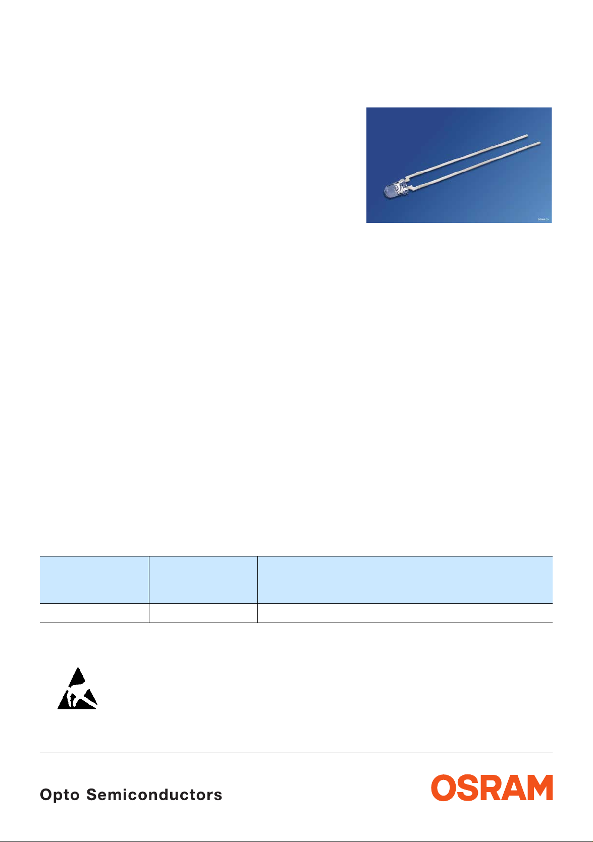
SFH 4350
Vorläufige Daten / Preliminary Data
Wesentliche Merkmale
• Infrarot LED mit hoher Ausgangsleistung
• Abstrahlwinkel ± 13°
• Sehr hohe Strahlstärke
• Emissionswellenlänge typ. 850 nm
Anwendungen
• Infrarotbeleuchtung für CMOS Kameras
• Sensorik
• Datenübertragung
Sicherheitshinweise
Je nach Betriebsart emittieren diese Bauteile
hochkonzentrierte, nicht sichtbare InfrarotStrahlung, die gefährlich für das menschliche
Auge sein kann. Produkte, die diese Bauteile
enthalten, müssen gemäß den Sicherheitsrichtlinien der IEC-Normen 60825-1 und 62471
behandelt werden.
Features
• High Power Infrared LED
• Emission angle ± 13°
• Very high radiant intensity
• Peak wavelength typ. 850 nm
Applications
• Infrared Illumination for CMOS cameras
• Sensor technology
• Data transmission
Safety Advices
Depending on the mode of operation, these
devices emit highly concentrated non visible
infrared light which can be hazardous to the
human eye. Products which incorporate these
devices have to follow the safety precautions
given in IEC 60825-1 and IEC 62471.
Typ
Type
SFH 4350 Q65110A2091 ≥ 40 (typ. 70)
1)
gemessen bei einem Raumwinkel Ω = 0.01 sr / measured at a solid angle of Ω = 0.01 sr
ATTENTION - Observe Precautions For Handling - Electrostatic Sensitive Device
2007-03-29 1
Bestellnummer
Ordering Code
Strahlstärkegruppierung1) (IF = 100 mA, tp = 20 ms)
Radiant Intensity Grouping
Ie (mW/sr)
1)
Page 2
Grenzwerte (TA = 25 °C) Maximum Ratings
SFH 4350
Bezeichnung
Parameter
Betriebs- und Lagertemperatur
Operating and storage temperature range
Sperrspannung
Reverse voltage
Vorwärtsgleichstrom
Forward current
Stoßstrom, tp = 10 μs, D = 0
Surge current
Verlustleistung
Power dissipation
Wärmewiderstand Sperrschicht - Umgebung bei
Montage auf FR4 Platine, Padgröße je 16 mm
2
Thermal resistance junction - ambient mounted
2
on PC-board (FR4), padsize 16 mm
each
Kennwerte (TA = 25 °C) Characteristics
Symbol
Symbol
Top , T
V
I
I
P
R
stg
R
F
FSM
tot
thJA
Wert
Value
Einheit
Unit
– 40 … + 100 °C
5 V
100 mA
1.5 A
180 mW
450
K/W
Bezeichnung
Parameter
Wellenlänge der Strahlung
Wavelength at peak emission
I
= 100 mA
F
Spektrale Bandbreite bei 50% von I
Spectral bandwidth at 50% of I
max
max
IF = 100 mA
Abstrahlwinkel
Half angle
Aktive Chipfläche
Active chip area
Abmessungen der aktiven Chipfläche
Dimension of the active chip area
Schaltzeiten, Ie von 10% auf 90% und von 90%
auf 10%, bei
Switching times, Ιe from 10% to 90% and from
90% to 10%,
I
= 100 mA, RL = 50 Ω
F
I
= 100 mA, RL = 50 Ω
F
Symbol
Symbol
λ
peak
Wert
Value
Einheit
Unit
850 nm
Δλ 35 nm
ϕ ± 13 Grad
deg.
A
L × B
0.09 mm
0.3 × 0.3 mm²
2
L × W
t
, t
r
f
12 ns
2007-03-29 2
Page 3
Kennwerte (TA = 25 °C)
Characteristics (cont’d)
SFH 4350
Bezeichnung
Parameter
Durchlassspannung
Forward voltage
I
= 100 mA, tp = 20 ms
F
I
= 1 A, tp = 100 µs
F
Sperrstrom
Reverse current
V
= 5 V
R
Gesamtstrahlungsfluss
Total radiant flux
I
= 100 mA, tp = 20 ms
F
Temperaturkoeffizient von Ie bzw. Φe,
I
= 100 mA
F
Temperature coefficient of Ie or Φe, IF = 100 mA
Temperaturkoeffizient von VF, IF = 100 mA
Temperature coefficient of VF, IF = 100 mA
Temperaturkoeffizient von λ, IF = 100 mA
Temperature coefficient of λ, IF = 100 mA
Symbol
Symbol
V
F
V
F
I
R
Φ
e typ
TC
I
TC
V
TC
λ
Wert
Value
1.5 (< 1.8)
2.4 (< 3.0)
not designed for
Einheit
Unit
V
V
μA
reverse
operation
50 mW
– 0.5 %/K
– 0.7 mV/K
+ 0.2 nm/K
2007-03-29 3
Page 4

SFH 4350
Strahlstärke Ie in Achsrichtung
1)
gemessen bei einem Raumwinkel Ω = 0.01 sr
Radiant Intensity Ie in Axial Direction
at a solid angle of Ω = 0.01 sr
Bezeichnung
Symbol Werte
Parameter
SFH 4350 -USFH 4350 -VSFH 4350
Strahlstärke
Radiant intensity
I
= 100 mA, tp = 20 ms
F
Strahlstärke
I
e min
I
e max
I
e typ
40
80
63
125
500 700 900 1100 mW/sr
Radiant intensity
I
= 1 A, tp = 100 μs
F
1)
Nur eine Gruppe in einer Verpackungseinheit (Streuung kleiner 2:1) /
Only one group in one packing unit (variation lower 2:1)
Abstrahlcharakteristik
Radiation Characteristics I
50˚
ϕ
= f (ϕ)
rel
1.0
0.8
0˚10˚20˚30˚40˚
OHF02499
Values
-AW
100
200
SFH 4350
-BW
160
320
Einheit
Unit
mW/sr
mW/sr
60˚
70˚
80˚
90˚
100˚
0.6
0.4
0.2
0
0˚ 20˚ 40˚ 60˚ 80˚ 100˚ 120˚0.40.60.81.0
2007-03-29 4
Page 5

Relative Spectral Emission
I
= f (λ)
rel
100
%
I
rel
80
60
40
20
OHL01714
I
e
Radiant Intensity
I
e
100 mA
= f (I
F
Single pulse, tp = 20 μs
OHL01715
I
I
e (100 mA)
1
10
e
0
10
5
-1
10
5
-2
10
5
SFH 4350
)
Max. Permissible Forward Current
I
= f (TA), R
F
125
Ι
mA
F
100
75
50
25
= 450 K/W
thJA
OHR00880
0
700
Forward Current IF = f (VF)
Single pulse, tp = 20 μs
0
10
A
I
F
-1
10
5
-2
10
5
-3
10
5
-4
10
0
0.5 1 1.5 2 2.5 V3
nm
950750 800 850
λ
OHL01713
V
F
-3
10
0
10
1
10
2
10
Permissible Pulse Handling
Capability
I
= f (τ), TA = 25 °C,
F
duty cycle D = parameter
t
T
P
=
OHF02505
t
P
T
10 10s10
1.6
A
I
F
1.4
1.2
1.0
D
=
D
0.005
0.01
0.02
0.8
0.033
0.05
0.1
0.6
0.4
0.2
0.5
1
0.2
0
1010 1010 10
I
mA
F
t
3
1055
I
F
210-1-2-3-4-5
p
0
0 20 40 60 80 100˚C
T
2007-03-29 5
Page 6

Maßzeichnung Package Outlines
SFH 4350
5.2 (0.205)
4.5 (0.177)
4.1 (0.161)
3.9 (0.154)
Chip position
3.1 (0.122)
0.6 (0.024)
0.4 (0.016)
spacing
2.54 (0.100)
Surface
not flat
0.4 (0.016)
0.7 (0.028)
2
1
3.3 (0.130)
0.8 (0.031)
1.8 (0.071)
1.2 (0.047)
Maße in mm (inch) / Dimensions in mm (inch).
Gehäuse / Package 3 mm, klares Gehäuse / 1/10", clear package
Anschlussbelegung
Pin configuration
1 = Anode / anode
2 = Kathode / cathode
0.4 (0.016)
6.3 (0.248)
5.9 (0.232)
2.9 (0.114)
0.6 (0.024)
0.4 (0.016)
4.0 (0.157)
3.6 (0.142)
GEMY6689
Empfohlenes Lötpaddesign Wellenlöten TTW
Recommended Solder Pad Design TTW Soldering
Anode
4.8 (0.189)
4 (0.157)
Maße in mm (inch) / Dimensions in mm (inch).
2007-03-29 6
OHLPY985
Page 7

Lötbedingungen Soldering Conditions Wellenlöten (TTW) (nach CECC 00802) TTW Soldering (acc. to CECC 00802)
300
C
250
T
200
150
100
235 C
CC... 130100
C... 260
1. Welle
1. wave
ca 200 K/s
10 s
5 K/s
2. Welle
2. wave
2 K/s
SFH 4350
OHLY0598
Normalkurve
standard curve
Grenzkurven
limit curves
Zwangskühlung
forced cooling
s
t
50
2 K/s
0
0
50 100 150 200 250
Published by
OSRAM Opto Semiconductors GmbH
Wernerwerkstrasse 2, D-93049 Regensburg
www.osram-os.com
© All Rights Reserved.
The information describes the type of component and shall not be considered as assured chara cteristics.
Terms of delivery and rights to change design reserved. Due to technical requirements components may contain
dangerous substances. For information on the types in question please contact our Sales Organization.
Packing
Please use the recycling operators known to you. We can also help you – get in touch with your nearest sales office.
By agreement we will take packing material back, if it is sorted. You must bear the costs of transport. For packing
material that is returned to us unsorted or wh ich we are not obliged to accept, we shall hav e to invoice you for any costs
incurred.
Components used in life-support devices or systems must be expressly authorized for such purpose! Critical
components 1 , may only be used in life-support devices or systems 2 with the express written approval of OSRAM OS.
1
A critical component is a component used in a life-support device or sys tem whose failure can reasonably be expected
to cause the failure of that life-support device or system, or to affec t its safety or e ffectiveness of that dev ice or system.
2
Life support devices or systems are intended (a) to be implanted in the h uman body, or (b) to support and/or maintain
and sustain human life. If they fail, it is reasonable to assume that the health of the user may be endangered.
2007-03-29 7
 Loading...