

Page 1
Infrarot-LED mit hoher Ausgangsleistung
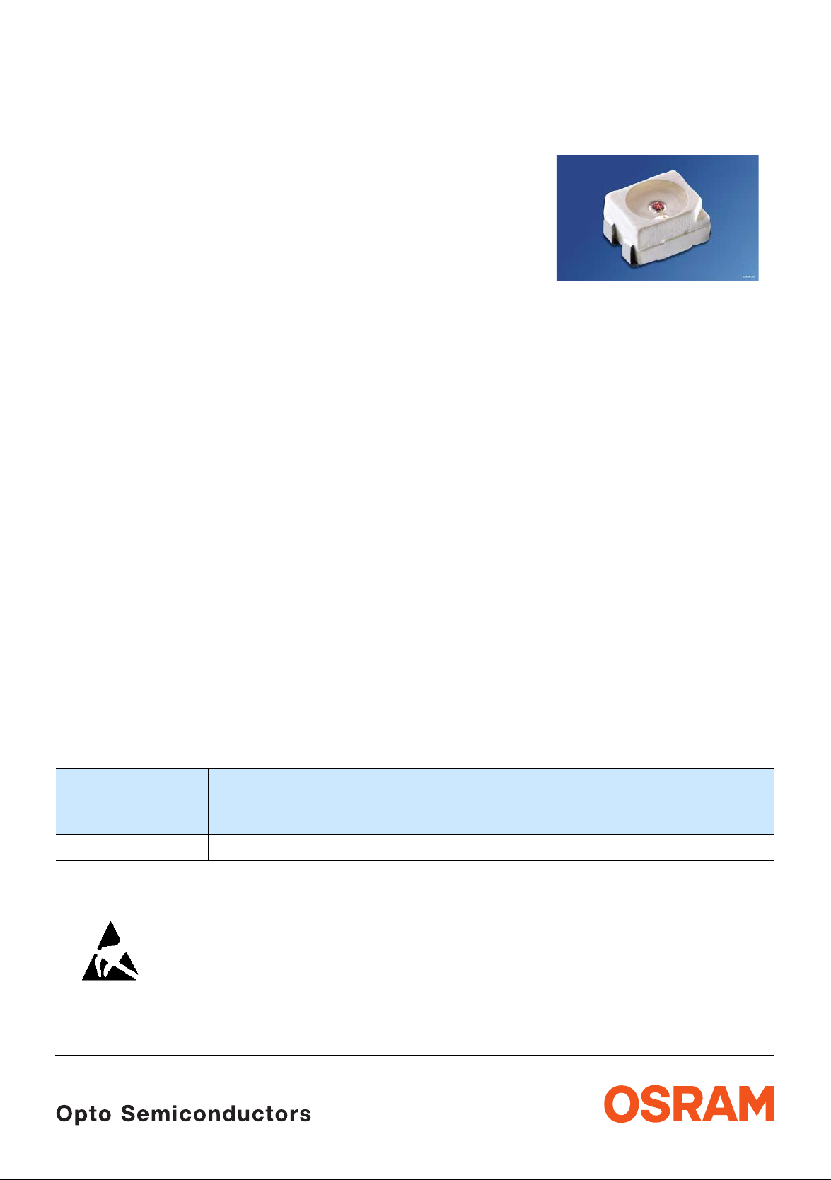
High Power Infrared LED
Lead (Pb) Free Product - RoHS Compliant
SFH 4250
preliminary data / vorläufige Daten
Wesentliche Merkmale
• Infrarot LED mit sehr hoher Ausgangsleistung
• Emissionswellenlänge typ. 850nm
• Hohe Bestromung bei hohen Temperaturen
möglich
Anwendungen
• Infrarotbeleuchtung für CMOS Kameras
• IR-Datenübertragung
• Sensorik
Sicherheitshinweise
Je nach Betriebsart emittieren diese Bauteile
hochkonzentrierte, nicht sichtbare InfrarotStrahlung, die gefährlich für das menschliche
Auge sein kann. Produkte, die diese Bauteile
enthalten, müssen gemäß den Sicherheitsrichtlinien der IEC-Norm 60825-1 behandelt
werden.
Features
• High Power Infrared LED
• Peak wavelength typ. 850nm
• High forward current allowed at high
temperature
Applications
• Infrared Illumination for CMOS cameras
• IR Data Transmission
• optical sensors
Safety Advices
Depending on the mode of operation, these
devices emit highly concentrated non visible
infrared light which can be hazardous to the
human eye. Products which incorporate these
devices have to follow the safety precautions
given in IEC 60825-1 “Safety of laser products”.
Typ
Type
SFH 4250 Q65110A2465 ≥ 10 (typ. 15)
1)
gemessen bei einem Raumwi nkel Ω = 0.01 sr / measured at a solid angle of Ω = 0.01 sr
ATTENTION - Observe Precautions For Handling - Electrostatic Sensitive Device
2005-02-21 1
Bestellnummer
Ordering Code
Strahlstärkegruppierung1) (IF = 100mA, tp = 20 ms)
Radiant Intensity Grouping
Ie (mW/sr)
1)
Page 2
Vorläufige Daten / Preliminary Data SFH 4250
Grenzwerte Maximum Ratings
Bezeichnung
Parameter
Betriebstemperatur
Operating temperature range
Lagertemperatur
Storage temperature range
Sperrspannung
Reverse voltage
Vorwärtsgleichstrom, TA ≤ 65 °C
Forward current
Stoßstrom, tp = 10 µs, D = 0, TA = 25 °C
Surge current
Verlustleistung TA = 25 °C
Power dissipation
Wärmewiderstand
Thermal resistance
Sperrschicht/Umgebung
Junction/ambient
Sperrschicht/Lötpad
Junction/soldering point
Montage auf PC-Board FR 4
2
(Padgröße
≥ 16 mm
)
mounted on PC board FR 4 (pad size ≥ 16 mm 2)
Symbol
Symbol
T
op
T
stg
V
R
I
F
I
FSM
P
tot
R
thJA
R
thJS
Wert
Value
Einheit
Unit
– 40 … + 100 °C
– 40 … + 100 °C
3 V
100 mA
1.5 A
180 mW
300
140
K/W
K/W
Kennwerte (TA = 25 °C) Characteristics
Bezeichnung
Parameter
Wellenlänge der Strahlung
Wavelength at peak emission
I
= 100 mA
F
Spektrale Bandbreite bei 50% von I
Spectral bandwidth at 50% of I
max
max
Symbol
Symbol
λ
∆λ 35 nm
IF = 100 mA
Abstrahlwinkel
Half angle
Aktive Chipfläche
Active chip area
2005-02-21 2
ϕ ± 60 Grad
A
peak
Wert
Value
Einheit
Unit
850 nm
deg.
0.09 mm
2
Page 3
Vorläufige Daten / Preliminary Data SFH 4250
Kennwerte (TA = 25 °C)
Characteristics (cont’d)
Bezeichnung
Parameter
Abmessungen der aktiven Chipfläche
Dimension of the active chip area
Schaltzeiten, Ie von 10% auf 90% und von 90%
I
auf 10%, bei
= 100 mA, RL = 50 Ω
F
Switching times, Ιe from 10% to 90% and from
I
90% to 10%,
= 100 mA, RL = 50 Ω
F
Durchlassspannung
Forward voltage
I
= 100 mA, tp = 20 ms
F
I
= 1 A, tp = 100 µs
F
Sperrstrom
Reverse current
V
= 3 V
R
Gesamtstrahlungsfluss
Total radiant flux
I
= 100 mA, tp = 20 ms
F
Temperaturkoeffizient von Ie bzw. Φe,
I
= 100 mA
F
Temperature coefficient of Ie or Φe, IF = 100 mA
Symbol
Symbol
L × B
L × W
t
, t
r
f
V
F
V
F
I
R
Φ
e
TC
I
Wert
Value
Einheit
Unit
0.3 × 0.3 mm
12 ns
1.5 (< 1.8)
2.4 (< 3.0)
V
V
0.01 (≤ 10) µA
40 mW
– 0.5 %/K
Temperaturkoeffizient von VF, IF = 100 mA
Temperature coefficient of VF, IF = 100 mA
Temperaturkoeffizient von λ, IF = 100 mA
Temperature coefficient of λ, IF = 100 mA
TC
TC
V
λ
– 0.7 mV/K
+ 0.2 nm/K
2005-02-21 3
Page 4

Vorläufige Daten / Preliminary Data SFH 4250
Strahlstärke Ie in Achsrichtung
1)
gemessen bei einem Raumwinkel Ω = 0.01 sr
Radiant Intensity Ie in Axial Direction
at a solid angle of Ω = 0.01 sr
Bezeichnung
Parameter
Strahlstärke
Radiant intensity
I
= 100 mA, tp = 20 ms
F
Strahlstärke
Radiant intensity
I
= 1 A, tp = 100 µs
F
1)
Nur eine Gruppe in einer Verpackungseinheit (Streuung kleiner2:1)
1)
Only one group in one packing unit, (variation lower 2:1)
Radiation Characteristics I
= f (ϕ)
rel
0˚10˚20˚40˚ 30˚
ϕ
1.0
Symbol Werte
Values
SFH 4250-R SFH 4250-S
I
e min
I
e max
I
e typ
OHL01660
10
20
16
32
100 140 mW/sr
Einheit
Unit
mW/sr
mW/sr
50˚
60˚
70˚
80˚
90˚
100˚
1.0 0.8 0.6 0.4
0.8
0.6
0.4
0.2
0
0˚ 20˚ 40˚ 60˚ 80˚ 100˚ 120˚
2005-02-21 4
Page 5

Vorläufige Daten / Preliminary Data SFH 4250
I
e
= f (I
OHL01715
)
F
Max. Permissible Forward Current
I
= f (TA), R
F
120
mA
100
I
F
80
60
40
20
= 300 K/W
thJA
OHL01716
Relative Spectral Emissi on
I
= f (λ)
rel
100
%
I
rel
80
60
40
20
OHL01714
Radiant Intensity
I
100 mA
e
Single pulse, tp = 20 µs
1
10
I
e
I
e (100 mA)
0
10
5
-1
10
5
-2
10
5
0
700
Forward Current IF = f (VF)
Single pulse, tp = 20 µs
0
10
A
I
F
-1
10
5
-2
10
5
-3
10
5
-4
10
0.5 1 1.5 2 2.5 V3
0
nm
950750 800 850
λ
OHL01713
V
F
-3
10
0
10
1
10
2
10
Permissible Pulse Handling
I
Capability
= f (τ), TA = 25 °C,
F
duty cycle D = parameter
t
P
T
=
OHF02505
t
P
T
10 10s10
t
1.6
A
I
F
1.4
1.2
1.0
0.8
0.6
0.4
D
=
D
0.005
0.01
0.02
0.033
0.05
0.1
0.2
0.5
1
0.2
0
1010 1010 10
I
mA
p
3
1055
F
I
F
210-1-2-3-4-5
0
0
40 60 80 120
20
˚C
2005-02-21 5
Page 6

Vorläufige Daten / Preliminary Data SFH 4250
Maßzeichnung Package Outlines
3.0 (0.118)
2.6 (0.102)
2.3 (0.091)
0.8 (0.031)
0.6 (0.024)
3.4 (0.134)
Maße werden wie folgt ange geben: mm (inch) / Dimensions are s pecified as follows: mm (inch).
2.1 (0.083)
AA
3.0 (0.118)
CA
Package marking
0.1 (0.004) (typ.)
(2.4) (0.095)
3.7 (0.146)
0.18 (0.007)
0.12 (0.005)
3.3 (0.130)
2.1 (0.083)
1.7 (0.067)
4˚±1
0.5 (0.020)
1.1 (0.043)
0.9 (0.035)
0.7 (0.028)
0.6 (0.024)
0.4 (0.016)
A A
AC
GPLY6084
Gehäuse / Package weiß, klarer Verguss / white, clear resin
Anschlussbelegung
pin configuration
2005-02-21 6
Kathode: abgeschrägte Ecke
Cathode: beveled edge
Page 7

Vorläufige Daten / Preliminary Data SFH 4250
Empfohlenes Lötpaddesign IR Flow Löten Recommended Solder Pad IR Reflow Soldering
Fläche darf elektrisch nicht beschaltet werden.
Padgeometrie für
verbesserte Wärmeableitung
Paddesign for
improved heat dissipation
2.3 (0.091)
0.8 (0.031)
1.1 (0.043)
3.7 (0.146)
0.7 (0.028)
1.5 (0.059)
3.3 (0.130)
Anode
Do not use this area for electrical contact.
3.3 (0.130)
11.1 (0.437)
Kathode/
Cathode
2
_
Fläche darf elektrisch nicht beschaltet werden.
Do not use this area for electrical contact.
Lötstoplack
Solder resist
Cu Fläche / 16 mm per pad
Cu-area
<
Empfohlenes Lötpaddesign Wellenlöten (TTW) Recommended Solder Pad TTW Soldering
Fläche darf elektrisch nicht beschaltet werden.
Do not use this area for electrical contact.
2 (0.079)
0.5 (0.020)
Kathode/
Cathode
Cu Fläche / > 16 mm per pad
Cu-area
6.1 (0.240)
2.8 (0.110)
2 (0.079)
6 (0.236)
2 (0.079)
3 (0.118)
Padgeometrie für
verbesserte Wärmeableitung
Paddesign for
improved heat dissipation
Anode
1 (0.039)
2.8 (0.110)
Fläche darf elektrisch nicht beschaltet werden.
Do not use this area for electrical contact.
OHLPY440
Bewegungsrichtung
der Platine
Lötstoplack
Solder resist
PCB-direction
2
OHAY1583
2005-02-21 7
Page 8

Vorläufige Daten / Preliminary Data SFH 4250
Lötbedingungen Vorbehandlung nach JEDEC Level 2 Soldering Conditions Preconditioning acc. to JEDEC Level 2 IR-Reflow Lötprofil für bleifreies Löten (nach J-STD-020B) IR Reflow Soldering Profile for lead free soldering (acc. to J-STD-020B)
300
˚C
250
T
255 ˚C
240 ˚C
Maximum Solder Profile
Recommended Solder Profile
Minimum Solder Profile
217 ˚C
200
10 s min
30 s max
150
120 s max
100 s max
Ramp Down
6 K/s (max)
100
Ramp Up
50
3 K/s (max)
25 ˚C
0
0
50 100 150 200 250 300
t
Wellenlöten (TTW) (nach CECC 00802) TTW Soldering (acc. to CECC 00802)
OHLA0687
260 ˚C
245 ˚C
235 ˚C
+0 ˚C
-5 ˚C
±5 ˚C
+5 ˚C
-0 ˚C
s
300
C
250
T
235 C
200
150
100
50
0
0
C... 260
1. Welle
1. wave
ca 200 K/s
CC... 130100
50 100 150 200 250
10 s
Zwangskühlung
2 K/s
forced cooling
5 K/s
2005-02-21 8
2. Welle
2. wave
OHLY0598
Normalkurve
standard curve
Grenzkurven
limit curves
2 K/s
s
t
Page 9

Vorläufige Daten / Preliminary Data SFH 4250
Published by
OSRAM Opto Semiconductors GmbH
Wernerwerkstrasse 2, D-93049 Regensburg
www.osram-os.com
© All Rights Reserved.
The information describes the type of component and sha ll not be c ons idered as assured characte ris tics .
Terms of delivery and rights to change design reserved. Due to technical requirements components may contain
dangerous substances . For in fo rmation on the types in question ple as e c ont ac t our Sales Organization.
Packing
Please use the recycling operators k nown to you . We can als o help you – get in touch wit h your near est sales offic e.
By agreement we will take p acking material back, if it is sorted. You m ust bear the costs of transport. For packing
material that is returned to us unsorted or which we are not obliged to accept, we shall have to invoice you for any costs
incurred.
Components used in life-su pport devices or systems must be expressly authorized fo r such purpose! Critical
components
1
A critical component is a co mponent usedin a l ife-support devi ce or system whose failure can re asonably be expec ted
1
, may only be used in life-support devices or systems 2 with the express written approval of OSRAM OS.
to cause the failure of that life-support device or system, or to affect its safety or effectiveness of that device or system.
2
Life support devices or systems are intend ed (a) to be impl anted i n t he human b ody , or (b ) to supp ort a nd/or ma inta in
and sustain human life. If th ey fail , it is rea so nable to assume that the health of the us er m ay be endangered.
2005-02-21 9
 Loading...