

Page 1
GaAs-IR-Lumineszenzdiode in SMT-Gehäuse
GaAs Infrared Emitter in SMT Package
SFH 420
SFH 425
3.0
2.6
2.3
2.1
3.0
3.4
0.8
0.6
Cathode/Collector marking
Approx. weight 0.03 g
(2.4)
2.8
2.4
2.54
Cathode/
Collector
Collector/Cathode marking
spacing
2.4
1.1
0.9
Anode/
Emitter
(typ)
0.1
3.3
3.7
1.1
0.18
0.12
Cathode/Collector
4.2
3.8
0.7
0.5
2.1
1.7
0.9
0.7
GPL06724
(2.85)
0.6
0.4
GPL06880
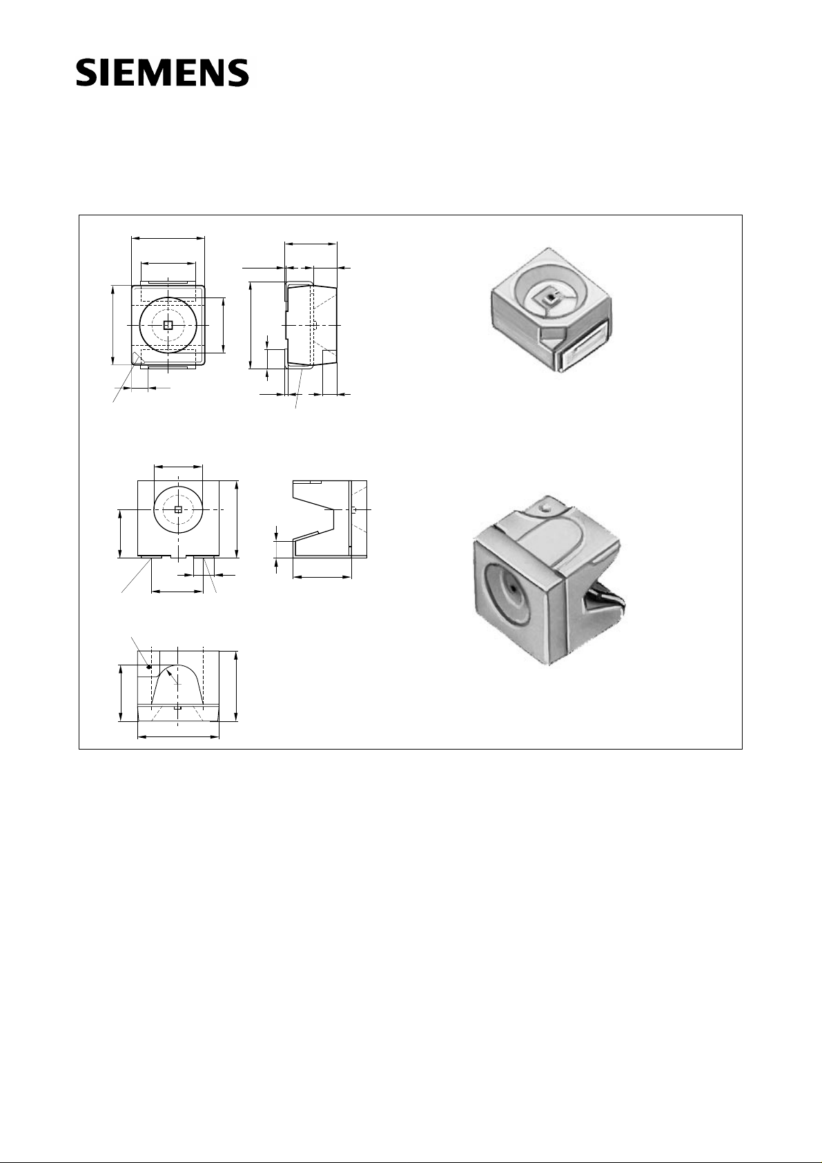
SFH 420 TOPLED
fpl06724fpl06867
(2.9)
(R1)
4.2
3.8
3.8
3.4
SFH 425 SIDELED
Maβe in mm, wenn nicht anders angegeben/Dimensions in mm, unless otherwise specified.
Wesentliche Merkmale
● GaAs-LED mit sehr hohem Wirkungsgrad
● Gute Linearität (I
= f [IF]) bei hohen Strömen
e
● Gleichstrom- (mit Modulation) oder
Impulsbetrieb möglich
● Hohe Zuverlässigkeit
● Hohe Impulsbelastbarkeit
● Oberflächenmontage geeignet
● Gegurtet lieferbar
● SFH 420 Gehäusegleich mit SFH 320/421
SFH 425 Gehäusegleich mit SFH 325/426
● SFH 425: Nur für IR-Reflow-Lötung geeignet.
Bei Schwallötung wenden Sie sich bitte an uns.
Features
● Very highly efficient GaAs-LED
● Good Linearity (I
= f [IF]) at high currents
e
● DC (with modulation) or pulsed operations
are possible
● High reliability
● High pulse handling capability
● Suitable for surface mounting (SMT)
● Available on tape and reel
● SFH 420 same package as SFH 320/421
SFH 425 same package as SFH 325/426
● SFH 425: Suitable only for IR-reflow
soldering. In case of dip soldering, please
contact us first.
Semiconductor Group 1 1997-11-01
Page 2

SFH 420
SFH 425
Anwendungen
● Miniaturlichtschranken für Gleich- und
Wechsellichtbetrieb, Lochstreifenlaser
● Industrieelektronik
● “Messen/Steuern/Regeln”
Typ
Type
SFH 420
SFH 425
Bestellnummer
Ordering Code
Q62702-P1690
Q62702-P0330
Grenzwerte (TA = 25 °C)
Maximum Ratings
Bezeichnung
Description
Betriebs- und Lagertemperatur
Operating and storage temperature range
Applications
● Miniature photointerrupters
● Industrial electronics
● For drive and control circuits
Gehäuse
Package
Kathodenkennzeichnung: abgesetzte Ecke
cathode marking: bevelled edge
TOPLED
SIDELED
Symbol
Symbol
T
; T
op
stg
Wert
Value
– 55 ... + 100 °C
Einheit
Unit
Sperrschichttemperatur
Junction temperature
Sperrspannung
Reverse voltage
Durchlaßstrom
Forward current
Stoßstrom, τ = 10 µs,
D = 0
Surge current
Verlustleistung
Power dissipation
Wärmewiderstand Sperrschicht - Umgebung bei
Montage auf FR4 Platine, Padgröße je 16 mm
2
Thermal resistance junction - ambient mounted on
PC-board (FR4), padsize 16 mm2 each
Wärmewiderstand Sperrschicht - Lötstelle bei
Montage auf Metall-Block
Thermal resistance junction - soldering point,
mounted on metal block
T
V
I
I
P
R
R
j
R
F
FSM
tot
thJA
thJS
100 °C
5V
100 mA
3A
160 mW
450
200
K/W
K/W
Semiconductor Group 2 1997-11-01
Page 3

Kennwerte (TA = 25 °C)
Characteristics
SFH 420
SFH 425
Bezeichnung
Description
Wellenlänge der Strahlung
Wavelength at peak emission
I
= 100 mA, tp = 20 ms
F
max
I
max
Spektrale Bandbreite bei 50% von
Spectral bandwidth at 50% of I
I
= 100 mA
F
Abstrahlwinkel
Half angle
Aktive Chipfläche
Active chip area
Abmessungen der aktiven Chipfläche
Dimension of the active chip area
Schaltzeiten, I
von 10 % auf 90 % und von
e
90 % auf 10 %, bei IF = 100 mA, RL = 50 Ω
Switching times, Ie from 10 % to 90 % and
from 90 % to 10 %, IF = 100 mA, RL = 50 Ω
Kapazität
Capacitance
V
= 0 V, f = 1 MHz
R
Durchlaβspannung
Forward voltage
I
= 100 mA, tp = 20 ms
F
I
= 1 A, tp = 100 µs
F
Sperrstrom
Reverse current
V
= 5 V
R
Gesamtstrahlungsfluβ
Total radiant flux
I
= 100 mA, tp = 20 ms
F
Temperaturkoeffizient von I
I
= 100 mA
F
bzw. Φe,
e
Temperature coefficient of Ie or Φe,
I
= 100 mA
F
Temperaturkoeffizient von
Temperature coefficient of V
Temperaturkoeffizient von λ,
VF, I
F
, I
F
F
I
= 100 mA
F
= 100 mA
= 100 mA
Temperature coefficient of λ, IF = 100 mA
Symbol
Symbol
λ
peak
Wert
Value
Einheit
Unit
950 nm
∆λ 55 nm
ϕ±60 Grad
deg.
A
L × B
L
× W
t
, t
r
f
C
o
V
F
V
F
I
R
Φ
e
TC
I
TC
V
TC
λ
0.09 mm
0.3 × 0.3 mm
0.5 µs
25 pF
1.3 (≤ 1.5)
2.3 (≤ 2.8)
V
V
0.01 (≤ 1)µA
14 mW
– 0.5 %/K
– 2 mV/K
+ 0.3 nm/K
2
Semiconductor Group 3 1997-11-01
Page 4

Gruppierung der Strahlstärke Ie in Achsrichtung
gemessen bei einem Raumwinkel Ω = 0.01 sr
Grouping at radiant intensity Ie in axial direction
at a solid angle of Ω = 0.01 sr
SFH 420
SFH 425
Bezeichnung
Description
Strahlstärke
Radiant intensity
I
= 100 mA, tp = 20 ms
F
Strahlstärke
Radiant intensity
I
= 1 A, tp = 100 µs
F
Relative spectral emission
I
= f (λ)
rel
100
%
Ι
rel
80
60
40
20
OHR01938
Symbol Werte
I
e
I
e typ.
Radiant intensity
Single pulse, t
2
10
A
Ι
e
Ι
e 100 mA
1
10
0
10
-1
10
= 20 µs
p
I
e
Ie100 mA
Einheit
Values
Unit
> 2.5 mW/sr
38 mW/sr
= f (IF)
OHR01551
Max. permissible forward current
I
= f (TA)
F
120
Ι
F
100
80
60
40
20
R
thjA
OHR00883
= 450 K/W
0
880 920 960 1000
Forward current
I
= f (VF), single pulse, tp = 20 µs
F
1
10
A
Ι
F
0
10
-1
10
-2
10
-3
10
1 2 3 4 V 5
nm
λ
OHR01554
V
F
1060
10
-3
10
-2
10-110010110A
Radiation characteristics S
50˚
60˚
70˚
80˚
90˚
100˚
1.0 0.8 0.6 0.4
rel
Ι
F
= f (ϕ)
0˚10˚20˚40˚ 30˚
ϕ
1.0
0.8
0.6
0.4
0.2
0
0˚ 20˚ 40˚ 60˚ 80˚ 100˚ 120˚
0
0
20 40 60 80 100 120mA˚C
T
OHL01660
A
-2
Semiconductor Group 4 1997-11-01
Page 5

Löthinweise
Soldering conditions
SFH 420
SFH 425
Bauform
Types
TOPLED
Tauch-, Schwall- und Schlepplötung
Dip, wave and drag soldering
Lötbadtemperatur
Temperature
of the
soldering
bath
260 °C
Maximal
zulässige
Lötzeit
Max. perm.
soldering
time
10 s
Abstand
Lötstelle –
Gehäuse
Distance
between
solder joint
and case
–
Reflowlötung
Reflow soldering
Lötzonentemperatur
Temperature
of soldering
zone
245 °C
Maximale
Durchlaufzeit
Max. transit
time
10 s
:
SIDELED
–
–
–
≥ 225 °C
10 s
Zusätzliche Informationen über allgemeine Lötbedingungen finden Sie im Datenbuch S. 103ff.
For additional information on generel soldering conditions please refer to our Data Book on
page 169ff.
Permissible pulse handling capability
I
= f (tp)
F
duty cycleD = parameter,T
4
10
mA
Ι
F
5
D
=
3
10
0.1
0.005
0.01
D
0.02
=
0.05
t
p
T
t
p
T
= 20 °C
A
OHR00860
Ι
F
0.2
5
0.5
DC
2
10
-5
-410-310-210-1100101102
10
10s
t
p
Semiconductor Group 5 1997-11-01
 Loading...