

Page 1
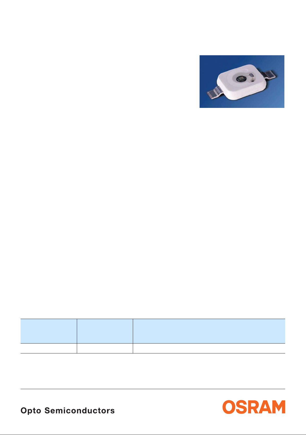
IR-Lumineszenzdiode (940 nm) mit hoher Ausgangsleistung
High Power Infrared Emitter (940 nm)
Lead (Pb) Free Product - RoHS Compliant
SFH 4231
Vorläufige Daten / Preliminary Data
Wesentliche Merkmale
• Punktlichtquelle mit hohem Wirkungsgrad bei
geringer Baugröße
• Chipgröße (emittierende Fläche) 1 x 1 mm2
• max. Gleichstrom 1 A
• niedriger Wärmewiderstand (15 K/W)
• Emissionswellenlänge 940 nm
• ESD-sicher bis 2 kV nach JESD22-A114-B
Anwendungen
• Infrarotbeleuchtung für CMOS Kameras
• Überwachungssysteme
• IR-Datenübertragung
• Fahrer-Assistenz Systeme
• Maschinensicherheit
Sicherheitshinweise
Je nach Betriebsart emittieren diese Bauteile
hochkonzentrierte, nicht sichtbare InfrarotStrahlung, die gefährlich für das menschliche
Auge sein kann. Produkte, die diese Bauteile
enthalten, müssen gemäß den Sicherheitsrichtlinien der IEC-Normen 60825-1 und 62471
behandelt werden.
Features
• Point lightsource with high efficiency and small
package
• die-size (emitting area) 1 x 1 mm2
• max. DC-current 1 A
• Low thermal resistance (15 K/W)
• Maximum of spectral emission at 940 nm
• ESD save up to 2 kV acc. to JESD22-A114-B
Applications
• Infrared Illumination for CMOS cameras
• Surveillance systems
• IR Data Transmission
• Driver assistance systems
• Machine security
Safety Advices
Depending on the mode of operation, these
devices emit highly concentrated non visible
infrared light which can be hazardous to the
human eye. Products which incorporate these
devices have to follow the safety precautions
given in IEC 60825-1 and IEC 62471.
Typ
Type
SFH 4231 Q65110A4808 typ. 500
1)
gemessen mit Ulbrichtkugel / measured with integrating sphere
2007-03-29 1
Bestellnummer
Ordering Code
Gesamtstrahlungsfluss1) (IF = 1A, tp = 100 µs)
Total Radiant Flux
Φe (mW)
1)
Page 2
Grenzwerte (TA = 25 °C) Maximum Ratings
SFH 4231
Bezeichnung
Parameter
Betriebs- und Lagertemperatur
Operating and storage temperature range
Sperrschichttemperatur
Junction temperature
Sperrspannung
Reverse voltage
Vorwärtsgleichstrom
Forward current
Stoßstrom, tp < 1 ms, D = 0.2
Surge current
Leistungsaufnahme
Power consumption
Wärmewiderstand Sperrschicht - Lötstelle bei
Montage auf Metall-Block
Thermal resistance junction - soldering point,
mounted on metal block
Symbol
Symbol
Top , T
T
V
I
I
P
R
stg
J
R
F
FSM
tot
thJS
Wert
Value
Einheit
Unit
– 40 … + 100 °C
+ 125 °C
1 V
1 A
2 A
2.4 W
15 K/W
Kennwerte (TA = 25 °C) Characteristics
Bezeichnung
Parameter
Wellenlänge der Strahlung
Wavelength at peak emission
I
= 1 A, tp = 10 ms
F
Centroid-Wellenlänge der Strahlung
Centroid wavelength
I
= 1 A, tp = 10 ms
F
Spektrale Bandbreite bei 50% von I
Spectral bandwidth at 50% of I
IF = 1 A, t
Abstrahlwinkel
= 10 ms
p
max
max
Half angle
Aktive Chipfläche
Active chip area
Abmessungen der aktiven Chipfläche
Dimension of the active chip area
Symbol
Symbol
λ
peak
λ
centroid
Wert
Value
Einheit
Unit
940 nm
935 nm
∆λ 45 nm
ϕ ± 60 Grad
deg.
A
L × B
1 mm
1 × 1 mm²
2
L × W
2007-03-29 2
Page 3
Kennwerte (TA = 25 °C)
Characteristics (cont’d)
SFH 4231
Bezeichnung
Parameter
Schaltzeiten, Ie von 10% auf 90% und von 90%
I
auf 10%,
= 1 A, RL = 50 Ω
F
Switching times, Ιe from 10% to 90% and from
I
90% to 10%,
= 1 A, RL = 50 Ω
F
Durchlassspannung
Forward voltage
I
= 1 A, tp = 100 µs
F
Strahlstärke
Radiant intensity
I
= 1 A, tp = 100 µs
F
Temperaturkoeffizient von Ie bzw. Φe
Temperature coefficient of Ie or Φe
I
= 1 A, tp = 10 ms
F
Temperaturkoeffizient von VF
Temperature coefficient of VF
I
= 1 A, tp = 10 ms
F
Temperaturkoeffizient von λ
Temperature coefficient of λ
I
= 1 A, tp = 10 ms
F
Symbol
Symbol
t
, t
r
f
V
F
I
e typ
TC
I
TC
V
TC
λ,centroid
Wert
Value
Einheit
Unit
20 ns
1.8 (< 2.4) V
200 mW/sr
– 0.5 %/K
– 1 mV/K
+ 0.2 nm/K
2007-03-29 3
Page 4

SFH 4231
Gesamtstrahlungsfluss1) Φ
Total Radiant Flux1) Φ
Bezeichnung
e
e
Symbol Werte
Parameter
Gesamtstrahlungsfluss
Total Radiant Flux
I
= 1 A, tp = 100 µs
F
1)
Nur eine Gruppe in einer Verpackungseinheit (Streuung kleiner 2:1) /
Only one group in one packing unit (variation lower 2:1)
Φ
Φ
e min
e max
Abstrahlcharakteristik
Radiation Characteristics I
50˚
= f (ϕ)
rel
ϕ
0˚10˚20˚40˚ 30˚
1.0
0.8
Values
SFH 4231-CX SFH 4231-DX
320
630
OHL01660
500
1000
Einheit
Unit
mW
mW
60˚
70˚
80˚
90˚
100˚
1.0 0.8 0.6 0.4
0.6
0.4
0.2
0
0˚ 20˚ 40˚ 60˚ 80˚ 100˚ 120˚
2007-03-29 4
Page 5

SFH 4231
Relative spektrale Emission
Relative Spectral Emission
I
= f (λ)
rel
100
%
I
rel
80
60
40
20
0
800
850 900 950 1025
OHF02895
nm
λ
Max. zulässiger Durchlassstrom
Max. Permissible Forward Current
I
= f (TA), R
F
1200
mA
I
F
800
600
400
= 15 K/W
thJS
OHF02801
Durchlassstrom
Forward Current
I
= f (VF)
F
Single pulse, tp = 100 µs
1
10
A
I
F
0
10
5
-1
10
5
-2
10
0 0.5
1 1.5 2 2.5 3V
OHF02894
V
F
Zulässige Impulsbelastbarkeit
Permissible Pulse Handling
Capability
I
= f (tp), T
F
≤ 85 °C,
A
Duty cycle D = parameter
2.5
A
I
F
2.0
1.5
1.0
OHF02803
D
=
0.005
0.01
0.02
0.05
0.1
0.2
0.5
1
Relativer Gesamtstrahlungsfluss
Relative Total Radiant Flux
Φe/Φe(1000mA) = f (IF)
Single pulse, tp = 100 µs
10
OHF02906
3
mA
I
4
1055
F
Φ
e
Φ
e (1000 mA)
1
10
0
10
5
-1
10
5
-2
10
5
-3
10
12
10 10
0.5
200
0
0˚C
20 40 60 80 100
T
S
0
t
P
t
P
=
D
T
T
1010 10
2007-03-29 5
I
F
-2-3-4-5
1010
10
10 s 10
t
p
210-1
Page 6

1)
Maßzeichnung Package Outlines
SFH 4231
0...0.1 (0.004)
A
6.2 (0.244)
5.8 (0.228)
Heat sink
0.29 (0.011)
0.24 (0.009)
(ø4.2 (0.165))
Protection
Diode
1.2 (0.047)
R1.5 (0.059)
11.2 (0.441)
10.8 (0.425)
0.8 (0.031)
Cathode
1.9 (0.075)
C
1.7 (0.067)
1.0 (0.039)
0.8 (0.031)
6.8 (0.268)
7.2 (0.283)
2.0 (0.079)
1.6 (0.063)
GPLY6192
Kathodenkennung: Markierung
Cathode mark: mark
Gewicht / Approx. weight: 0.2 g
Gurtung / Polarität und Lage Verpackungseinheit 800/Rolle, ø180 mm Method of Taping / Polarity and Orientation Packing unit 800/reel, ø180 mm
Cathode/Collector Side
4 (0.157)
1.55 (0.061)
2 (0.079)
1.75 (0.069)
6.35 (0.250)
8 (0.315)
1)
Maße in mm (inch) / Dimensions in mm (inch)
2007-03-29 6
11.5 (0.453)
12.4 (0.488)
24 (0.945)
0.3 (0.012)
0.3 (0.012)
7.35 (0.289)
1.9 (0.075)
OHAY0508
Page 7

Empfohlenes Lötpaddesign Recommended Solder Pad Design
SFH 4231
12.0 (0.472)
11.6 (0.457)
0.3 (0.012)
ø2.5 (0.098)
ø4.0 (0.157)
Kupfer
Copper
Lötstopplack
Solder resist
Lötpasten Schablone
Solder paste stencil
Bare Copper
Freies Kupfer
1.6 (0.063)
2.3 (0.091)
10 (0.394)
11.6 (0.457)
1.6 (0.063)
ø4.0 (0.157)
Heatsink attach
Footprint
2.3 (0.091)
3 Lötstellen
3 solder points
Thermisch optimiertes PCB
Thermal enhanced PCB
OHAY0681
Achtung:
Anode und Heatsink sind elektrisch verbunden
Attention:
Anode and Heatsink are electrically connected
2007-03-29 7
Page 8

SFH 4231
Lötbedingungen Vorbehandlung nach JEDEC Level 4
Soldering Conditions Preconditioning acc. to JEDEC Level 4
Reflow Lötprofil für bleifreies Löten (nach J-STD-020C)
Reflow Soldering Profile for lead free soldering (acc. to J-STD-020C)
300
˚C
250
T
255 ˚C
240 ˚C
Maximum Solder Profile
Recommended Solder Profile
Minimum Solder Profile
217 ˚C
200
10 s min
OHLA0687
260 ˚C
245 ˚C
235 ˚C
+0 ˚C
-5 ˚C
±5 ˚C
+5 ˚C
-0 ˚C
30 s max
150
120 s max
100 s max
Ramp Down
6 K/s (max)
100
Ramp Up
50
3 K/s (max)
25 ˚C
0
0
50 100 150 200 250 300
s
t
Published by
OSRAM Opto Semiconductors GmbH
Wernerwerkstrasse 2, D-93049 Regensburg
www.osram-os.com
© All Rights Reserved.
The information describes the type of component and shall not be considered as assured characteristics.
Terms of delivery and rights to change design reserved. Due to technical requirements components may contain
dangerous substances. For information on the types in question please contact our Sales Organization.
Packing
Please use the recycling operators known to you. We can also help you – get in touch with your nearest sales office.
By agreement we will take packing material back, if it is sorted. You must bear the costs of transport. For packing
material that is returned to us unsorted or which we are not obliged to accept, we shall have to invoice you for any costs
incurred.
Components used in life-support devices or systems must be expressly authorized for such purpose! Critical
components
1
A critical component is a component usedin a life-support device or system whose failure can reasonably be expected
1
, may only be used in life-support devices or systems 2 with the express written approval of OSRAM OS.
to cause the failure of that life-support device or system, or to affect its safety or effectiveness of that device or system.
2
Life support devices or systems are intended (a) to be implanted in the human body, or (b) to support and/or maintain
and sustain human life. If they fail, it is reasonable to assume that the health of the user may be endangered.
2007-03-29 8
 Loading...