

Page 1
.
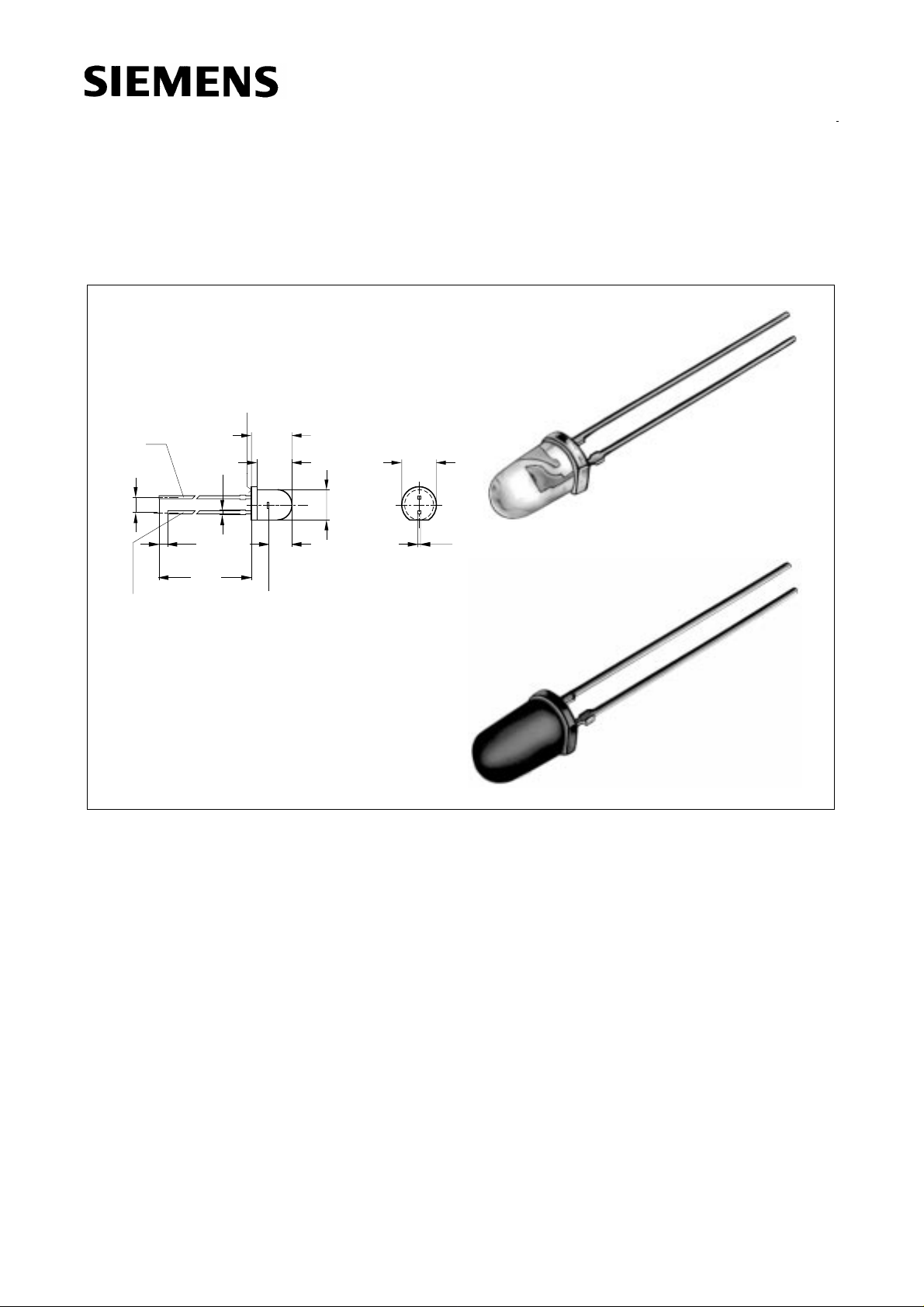
Neu: NPN-Silizium-Fototransistor
New: Silicon NPN Phototransistor
Area not flat
0.8
6.9
6.1
5.7
5.5
0.4
ø5.1
4.0
3.4
Chip position
5.9
5.5
ø4.8
GEX06630
0.6
0.4
spacing
2.54 mm
Cathode (Diode)
Collector (Transistor)
Approx. weight 0.4 g
1.8
1.2
29.5
27.5
SFH 314
SFH 314 FA
SFH 314
SFH 314 FA
0.6
0.4
Maße in mm, wenn nicht anders angegeben/Dimensio ns in mm , unless otherwise specified.
Wesentliche Merkmale
● Speziell geeignet für Anwendungen im
Bereich von 460 nm bis 1080 nm (SFH 314)
und bei 880 nm (SFH 314 FA)
● Hohe Linearität
● 5 mm-Plastikbauform
Anwendungen
● Computer-Blitzlichtgeräte
● Lichtschranken für Gleich- und
Wechsellichtbetrieb
● Industrieelektronik
● “Messen/Steuern/Regeln”
Features
● Especially suitable for applications from
460 nm to 1080 nm (SFH 314) and of
880 nm (SFH 314 FA)
● High linearity
● 5 mm plastic package
Applications
● Computer-controlled flashes
● Photointerrupters
● Industrial electronics
● For control and drive circuits
feof6652 feo06652
Semiconductor Group 1 1997-11-27
Page 2
Typ
Type
SFH 314
SFH 314 FA
Bestellnummer
Ordering Code
SFH 314
SFH 314-2
SFH 314-3
SFH 314 FA
SFH 314 FA-2
SFH 314 FA-3
Q62702-P1668
Q62702-P1755
Q62702-P1756
Q62702-P1675
Q62702-P1757
Q62702-P1758
Grenzwerte
Maximum Ratings
Bezeichnung
Description
Betriebs- und Lagertemperatur
Operating and storage temperature range
Löttemperatur bei Tauchlötung
Lötstelle ≥ 2 mm vom Gehäuse,
Lötzeit
t ≤ 5 s
Dip soldering temperature ≥ 2 mm distance
from case bottom, soldering time
t ≤ 5 s
Symbol
Symbol
T
; T
op
stg
T
S
Wert
Value
Einheit
Unit
– 55 ... + 100 °C
260 °C
Löttemperatur bei Kolbenlötung
Lötstelle ≥ 2 mm vom Gehäuse,
Lötzeit
t ≤ 3 s
Iron soldering temperature ≥ 2 mm distance
from case bottom
t ≤ 3 s
Kollektor-Emitterspannung
Collector-emitter voltage
Kollektorstrom
Collector current
Kollektorspitzenstrom, τ < 10 µs
Collector surge current
Emitter-Kollektorspannung
Emitter-collector voltage
Verlustleistung,
T
= 25 °C
A
Total power dissipation
Wärmewiderstand
Thermal resistance
T
S
V
CE
I
C
I
CS
V
EC
P
tot
R
thJA
300 °C
70 V
50 mA
100 mA
7V
200 mW
375 K/W
Semiconductor Group 2 1997-11-27
Page 3

Kennwerte (TA = 25 °C, λ = 950 nm)
Characteristics
SFH 314
SFH 314 FA
Bezeichnung
Description
Wellenlänge der max. Fotoempfindlichkeit
Wavelength of max. sensitivity
Spektraler Bereich der Fotoempfindlichkeit
S = 10 % von S
max
Spectral range of sensitivity
S = 10 % of S
max
Bestrahlungsempfindliche Fläche
Radiant sensitive area
Abmessung der Chipfläche
Dimensions of chip area
Abstand Chipoberfläche zu Gehäuseoberfläche
Distance chip front to case surface
Halbwinkel
Half angle
Symbol
Symbol
Wert
Value
Einheit
Unit
SFH 314 SFH 314 FA
λ
S max
850 870 nm
λ 460 ... 1080 740 ... 1080 nm
A
L × B
L
× W
H
0.55 0.55 mm
1 × 11×1mm×mm
3.4 ... 4.0 3.4 ... 4.0 mm
ϕ±40 ± 40 Grad
deg.
2
Kapazität,
V
= 0 V, f = 1 MHz, E = 0
CE
Capacitance
Dunkelstrom
Dark current
V
= 10 V, E = 0
CE
Fotostrom,
Photocurrent
E
= 0.5 mW/cm2, VCE = 5 V
e
E
= 1000 Ix, Normlicht/standard light A,
v
V
= 5 V
CE
C
I
I
I
CE
CEO
PCE
PCE
15 15 pF
10 (≤ 200) 10 (≤ 200) nA
≥ 0.63
7
≥ 0.63
–
mA
mA
Semiconductor Group 3 1997-11-27
Page 4

SFH 314
SFH 314 FA
Die Fototransistoren werden nach ihrer Fotoempfindlichkeit gruppiert und mit arabischen
Ziffern gekennzeichnet.
The phototransistors are grouped according to their spectral sensitivity and distinguished
by arabian figures.
Bezeichnung
Description
Fotostrom, λ = 950 nm
Photocurrent
E
= 0.5 mW/cm2, VCE = 5 V
e
SFH 314:
E
= 1000 Ix, Normlicht/
v
standard light A,
V
= 5 V
CE
Anstiegszeit/Abfallzeit
Rise and fall time
I
= 1 mA, VCC = 5 V,
C
R
= 1 kΩ
L
Kollektor-Emitter-
Sättigungsspannung
Collector-emitter saturation
voltage
PCEmin
1)
× 0.3,
2
I
= I
C
E
= 0.5 mW/cm
e
Symbol
Symbol
I
PCE
I
PCE
t
, t
r
f
V
CEsat
Wert
Value
Einheit
Unit
-1 -2 -3 -4
0.63 ... 1.25
3.4
1...2
5.4
1.6 ... 3.2
8.6
≥ 2.5
13.5
mA
mA
8101214µs
150 150 150 150 mV
1)
I
ist der minimale Fotostrom der jeweiligen Gruppe
PCEmin
1)
Directional characteristics S
50
60
I
is the min. photocurrent of the specified group
PCEmin
70
80
90
100
= f (ϕ)
rel
ϕ
10203040
0
1.0
0.8
0.6
0.4
0.2
0
02040 60 80 100 1200.40.60.81.0
OHF02329
Semiconductor Group 4 1997-11-27
Page 5

T
= 25 °C, λ = 950 nm
A
Rel. spectral sensitivity SFH 314 S
100
S
rel
%
80
70
60
50
40
30
20
10
0
400
500 600 700 800 900 nm 1100
Photocurrent I
V
= 5 V, normalized to 25oC
CE
1.6
Ι
PCE
Ι
25
PCE
1.4
1.2
PCE
= f (TA),
OHF02332
λ
OHF01524
rel
=f (λ)
Rel. spectr.sensitivity SFH 314 FA,S
100
S
rel
%
80
70
60
50
40
30
20
10
0
400
500 600 700 800 900 nm 1100
Photocurrent
I
= f (Ee), VCE= 5 V
PCE
1
10
mA
Ι
PCE
0
10
OHF02331
λ
OHF02339
rel
=f(λ)
Dark current I
2
10
nA
Ι
CEO
1
10
0
10
-1
10
-2
10
0
CEO
10 20 30 40 50 70V
Collector-emitter capacitance
CCE= f (VCE), f = 1 MHz
50
C
CE
pF
40
SFH 314
SFH 314 FA
= f (VCE), E = 0
OHF02341
V
CE
OHF02344
1.0
0.8
0.6
0.4
0.2
0
0 25 50 75 100
-25
Photocurrent
I
= f (VCE), Ee = parameter
PCE
1
10
mA
Ι
PCE
0
10
-1
10
0
10 20 30 40 50 V 70
30
-1
10
-2
10
-3
10
C
T
A
-3 -2
10
10
Total power dissipation
P
= f (TA)
tot
OHF02338
mW
1
2
cm
0.5
0.25
0.1
mW
cm
mW
cm
mW
cm
2
2
2
250
mW
P
tot
200
150
100
50
2
10mW/cm
E
e
OHF02340
0
20
10
0
-2 -1
10
10010110 102V
Dark current
I
= f (TA), VCE= 10 V, E = 0
CEO
2
10
nA
Ι
CEO
1
10
0
10
-1
10
V
CE
OHF02342
-2
0
0 20 40 60 80 ˚C 100
V
CE
T
A
10
0
20 40 60 80 100˚C
T
A
Semiconductor Group 5 1997-11-27
 Loading...