

Page 1
SFH 309 P
SFH 309 PFA
NPN-Silizium-Fototransistor
Silicon NPN Phototransistor
SFH 309 P
SFH 309 PFA
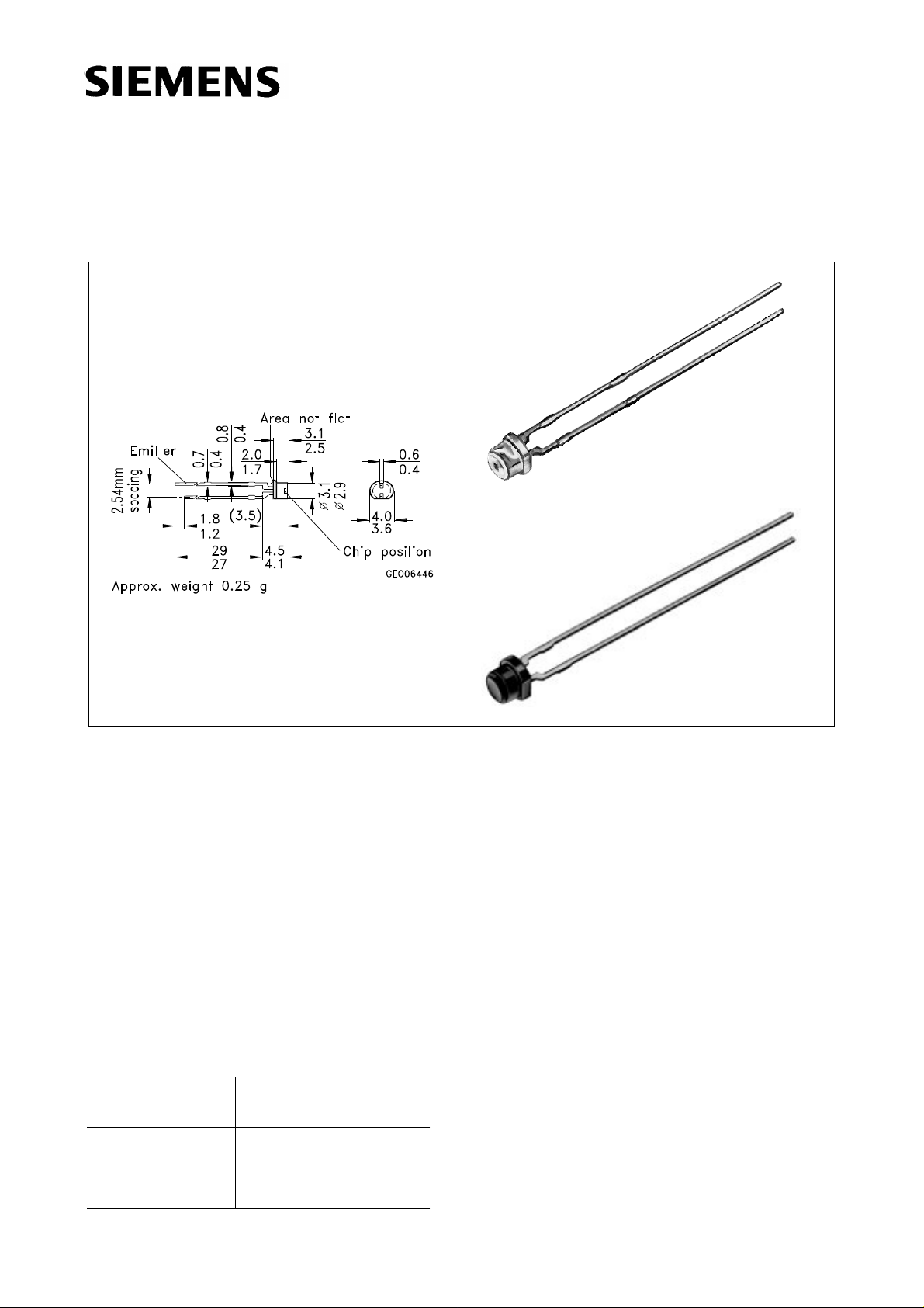
feo06445feof6445
Maße in mm, wenn nicht anders angegeben/Dimensions in mm, unless otherwise specified
Wesentliche Merkmale
● Speziell geeignet für Anwendungen im
Bereich von 380 nm bis 1180 nm
(SFH 309 P) und bei 880 nm (SFH 309 PFA)
● Hohe Linearität
● 3 mm plane Plastikbauform im LED-Gehäuse
● Gruppiert lieferbar
Anwendungen
● Lichtschranken für Gleich- und
Wechsellichtbetrieb
● Industrieelektronik
● “Messen/Steuern/Regeln”
Typ (*vorher)
Type (*formerly)
Bestellnummer
Ordering Code
Features
● Especially suitable for applications from
380 nm to 1180 nm (SFH 309 P) and of
880 nm (SFH 309 PFA)
● High linearity
● 3 mm plane LED plastic package
● Available in groups
Applications
● Photointerrupters
● Industrial electronics
● For control and drive circuits
SFH 309 P Q62702-P245
SFH 309 PFA
Q62702-P246
(*SFH 309 PF)
Semiconductor Group 1
01.97
Page 2
Grenzwerte
Maximum Ratings
SFH 309 P
SFH 309 PFA
Bezeichnung
Description
Betriebs- und Lagertemperatur
Operating and storage temperature range
Löttemperatur bei Tauchlötung
Lötstelle ≥ 2 mm vom Gehäuse,
Lötzeit
t ≤ 5 s
Dip soldering temperature ≥ 2 mm distance
from case bottom, soldering time t ≤ 5 s
Löttemperatur bei Kolbenlötung
Lötstelle ≥ 2 mm vom Gehäuse,
Lötzeit
t ≤ 3 s
Iron soldering temperature ≥ 2 mm distance
from case bottom, soldering time t ≤ 3 s
Kollektor-Emitterspannung
Collector-emitter voltage
Kollektorstrom
Collector current
Kollektorspitzenstrom, τ < 10 µs
Collector surge current
Symbol
Symbol
T
; T
op
stg
T
S
T
S
V
CE
I
C
I
CS
Wert
Value
Einheit
Unit
– 55 ... + 100 °C
260 °C
300 °C
35 V
15 mA
75 mA
T
Verlustleistung,
= 25 °C
A
Total power dissipation
Wärmewiderstand
Thermal resistance
P
tot
R
thJA
165 mW
450 K/W
Semiconductor Group 2
Page 3

Kennwerte (TA = 25 °C, λ = 950 nm)
Characteristics
SFH 309 P
SFH 309 PFA
Bezeichnung
Description
Wellenlänge der max. Fotoempfindlichkeit
Wavelength of max. sensitivity
Spektraler Bereich der Fotoempfindlichkeit
S = 10 % von S
max
Spectral range of sensitivity
S = 10 % of S
max
Bestrahlungsempfindliche Fläche (∅ 240 µm)
Radiant sensitive area
Abmessung der Chipfläche
Dimensions of chip area
Abstand Chipoberfläche zu Gehäuseoberfläche
Distance chip front to case surface
Halbwinkel
Half angle
Symbol
Symbol
Wert
Value
Einheit
Unit
SFH 309 P SFH 309 PFA
λ
S max
860 900 nm
λ 380 ... 1180 730 ... 1120 nm
A 0.045 0.045 mm
L × B
L
× W
H
ϕ±75 ± 75 Grad
0.45 × 0.45 0.45 × 0.45 mm × mm
0.4 ... 0.8 0.4 ... 0.8 mm
deg.
2
Kapazität,
V
Capacitance
Dunkelstrom
Dark current
V
= 25 V, E = 0
CE
= 0 V, f = 1 MHz, E = 0
CE
C
I
CE
CEO
5.0 5.0 pF
1 (≤ 200) 1 (≤ 200) nA
Semiconductor Group 3
Page 4

SFH 309 P
SFH 309 PFA
Bezeichnung
Description
Fotostrom, λ = 950 nm
Photocurrent
E
= 0.5 mW/cm2, VCE = 5 V
e
SFH 309 P:
E
= 1000 Ix, Normlicht/standard light A,
v
V
= 5 V
CE
Anstiegszeit/Abfallzeit
Rise and fall time
I
= 1 mA, VCC = 5 V, RL = 1 kΩ
C
Kollektor-Emitter-Sättigungsspannung
Collector-emitter saturation voltage
I
= 20 µA , Ee = 0.5 mW/cm
C
2
Symbol
Symbol
I
PCE
I
PCE
t
, t
r
f
V
CEsat
Wert
Value
≥ 63
420
Einheit
Unit
µA
µA
≥ 6 µs
150 mV
Directional characteristics S
rel
= f (ϕ)
Semiconductor Group 4
Page 5

SFH 309 P
SFH 309 PFA
Relative spectral sensitivity,
SFH 309 P S
rel
= f (λ)
Total power dissipation
P
= f (TA)
tot
Relative spectral sensitivity,
SFH 309 PFA S
rel
= f (λ)
Photocurrent
I
= f (VCE), Ee= Parameter
PCE
Photocurrent
I
= f (Ee), VCE= 5 V
PCE
Dark current
I
= f (VCE), E = 0
CEO
Dark current
I
= f (TA), VCE = 25 V, E = 0
CEO
Capacitance
C
= f (VCE), f = 1 MHz, E = 0
CE
Semiconductor Group 5
Photocurrent
I
PCE/IPCE25
o
= f (TA), VCE= 5 V
 Loading...