

Page 1
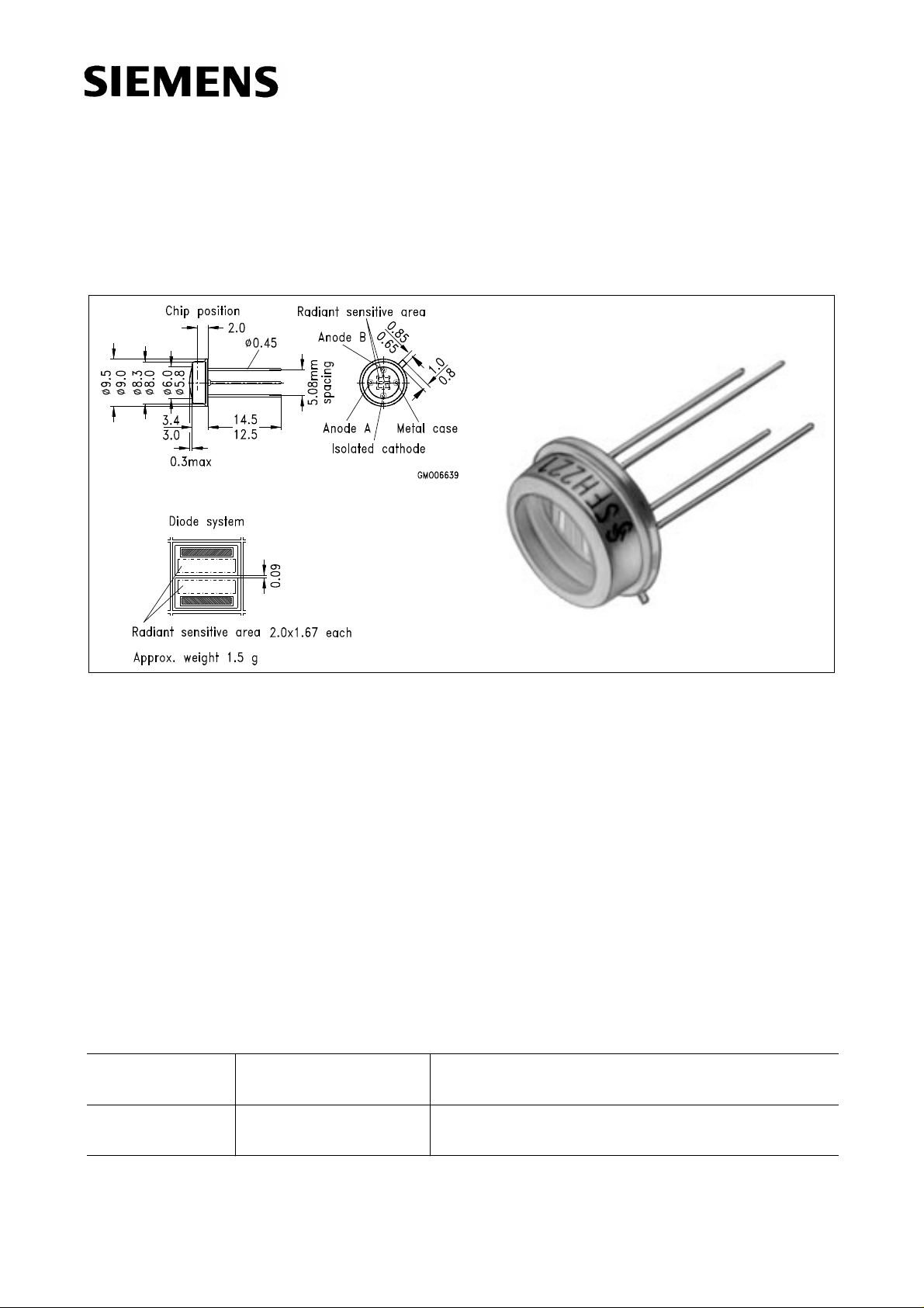
SFH 221 S
Silizium-Differential-Fotodiode
Silicon Differential Photodiode
SFH 221 S
Maβe in mm, wenn nicht anders angegeben/Dimensions in mm, unless otherwise specified.
Wesentliche Merkmale
● Speziell geeignet für Anwendungen im
Bereich von 400 nm bis 1100 nm
● Hohe Fotoempfindlichkeit
● Hermetisch dichte Metallbauform (ähnlich
TO-5), geeignet bis 125oC
● Doppeldiode von extrem hoher
1)
Gleichmäβigkeit
Anwendungen
● Nachlaufsteuerungen
● Kantenführung
● Industrieelektronik
● “Messen/Steuern/Regeln”
Typ (*ab 4/95)
Type (*as of 4/95)
SFH 221 S
Bestellnummer
Ordering Code
Q62702-P270 Lötspieβe im 5.08-mm-Raster (
(*SFH 221)
1)
Eine Abstimmung der Einsatzbedingungen mit dem Hersteller wird empfohlen bei TA > 85oC
1)
For operating conditions of TA > 85oC please contact us.
Features
● Especially suitable for applications from
400 nm to 1100 nm
● High photosensitivity
● Hermetically sealed metal package (similar
to TO-5), suitable up to 125oC
● Double diode with extremely high
homogeneousness
Applications
● Follow-up controls
● Edge drives
● Industrial electronics
● For control and drive circuits
Gehäuse
Package
2
/10”)
solder tabs 5.08 mm (2/10”) lead spacing
1)
Semiconductor Group 399
Page 2
Grenzwerte
Maximum Ratings
SFH 221 S
Bezeichnung
Description
Betriebs- und Lagertemperatur
Symbol
Symbol
T
; T
op
stg
Wert
Value
–40 ... +80
Operating and storage temperature range
Löttemperatur (Lötstelle 2 mm vom
T
S
230
Gehäuse entfernt bei Lötzeit t ≤ 3s)
Soldering temperature in 2 mm distance
from case bottom (t ≤ 3s)
Sperrspannung
V
R
10 V
Reverse voltage
Isolationsspannung gegen Gehäuse
V
IS
100 V
Insulation voltage vs. package
Verlustleistung, T
= 25oC
A
P
tot
50 mW
Total power dissipation
Kennwerte (T
= 25oC, Normlicht A, T = 2856 K) für jede Einzeldiode
A
Characteristics (TA = 25oC, standard light A, T = 2856 K) per single diode
Einheit
Unit
o
C
o
C
Bezeichnung
Description
Fotoempfindlichkeit, V
= 5 V
R
Spectral sensitivity
Wellenlänge der max. Fotoempfindlichkeit
Wavelength of max. sensitivity
Spektraler Bereich der Fotoempfindlichkeit
S = 10% von S
max
Spectral range of sensitivity
S = 10% of S
max
Bestrahlungsempfindliche Fläche
Radiant sensitive area
Abmessung der bestrahlungsempfindlichen
Fläche
Dimensions of radiant sensitive area
Abstand Chipoberfläche zu Gehäuseoberfläche
Distance chip front to case surface
Halbwinkel
Half angle
Symbol
Symbol
Wert
Value
Einheit
Unit
S 24 (≥ 15) nA/Ix
λ
S max
900 nm
λ 400 ... 1100 nm
A 1.54 mm
L x B
0.7 x 2.2 mm
L x W
H 1.1 ... 1.6 mm
ϕ±55 Grad
deg.
2
Semiconductor Group 400
Page 3

Kennwerte (TA = 25oC, Normlicht A, T = 2856 K) für jede Einzeldiode
Characteristics (TA = 25oC, standard light A, T = 2856 K) per single diode
SFH 221 S
Bezeichnung
Description
Dunkelstrom, VR = 10 V
Dark current
Spektrale Fotoempfindlichkeit, λ = 850 nm
Spectral sensitivity
Maximale Abweichung der
Fotoempfindlichkeit vom Mittelwert
Max. deviation of the system spectral
sensitivity from the average
Quantenausbeute, λ = 850 nm
Quantum yield
Leerlaufspannung, E
= 1000 Ix
v
Open-circuit voltage
Kurzschluβstrom, E
= 1000 Ix
v
Short-circuit current
Isolationsstrom, V
= 100 V
IS
Insulation current
Symbol
Symbol
I
R
S
λ
Wert
Value
Einheit
Unit
10 (≤ 100) nA
0.55 A/W
∆S ± 5%
η 0.80 Electrons
Photon
V
L
I
K
I
IS
330 (≥ 280) mV
24 µA
0.1 (≤ 1) nA
Anstiegs und Abfallzeit des Fotostromes
Rise and fall time of the photocurrent
R
= 1 kΩ; VR= 5 V; λ = 850 nm; Ip = 25 µA
L
Durchlaβspannung, I
= 40 mA, E = 0
F
Forward voltage
Kapazität, V
= 0 V, f = 1 MHz, E = 0
R
Capacitance
Temperaturkoeffizient für V
Temperature coefficient of V
Temperaturkoeffizient für I
Temperature coefficient of I
L
L
K
K
Rauschäquivalente Strahlungsleistung
Noise equivalent power
= 10 V, λ = 850 nm
V
R
Nachweisgrenze, V
= 10 V, λ = 850 nm
R
Detection limit
tr, t
V
F
C
0
TC
TC
f
V
I
500 ns
1.0 V
25 pF
–2.6 mV/K
0.18 %/K
NEP 1.0 x 10
D* 1.2 x 10
–13
12
W
√Hz
cm · √Hz
W
Semiconductor Group 401
Page 4

SFH 221 S
Relative spectral sensitivity
S
= f (λ)
rel
Dark current
I
= f (VR), E = 0
R
Photocurrent IP= f (Ev), VR = 5 V
Open-circuit-voltage V
= f (Ev)
L
Capacitance
C = f (V
), f = 1 MHz, E = 0
R
Total power dissipation
P
= f (TA)
tot
Dark current
I
= f (TA), VR= 1 V, E = 0
R
Directional characteristics S
rel
= f (ϕ)
Semiconductor Group 402
 Loading...