

Page 1

SERCON410B
DATASHEET
Page 2

USE IN LIFE SUPPORT DEVICESOR SYSTEMSMUSTBEEXPRESSLYAUTHORIZED.
SGS-THOMSON PRODUCTS ARE NOT AUTHORIZED FOR USE AS CRITICAL COMPONENTS IN LIFE SUPPORT
DEVICES OR SYSTEMS WITHOUT THE EXPRESS WRITTEN APPROVAL OF SGS-THOMSON Microelectronics.
As used herein :
1. Life support devices or systems are those which (a) are
intended for surgical implant into the body,or (b)support
or sustain life, and whose failure to perform, when properly used in accordance with instructions for use provided with the product, can be reasonably expected to
result in significant injury to the user.
2. A critical component is any component of a life support
device or system whose failure to perform can reasonably be expected to cause the failure of the life support
device or system, or to affect its safety or effectiveness.
Page 3

SERCON410BDATASHEET
INDEX
Page
Number
SERCON410B .................................... 1
1 GENERALDESCRIPTION ............................... 5
2 PIN DESCRIPTION ........................................ 6
3 ELECTRICALCHARACTERISTICS ............................... 9
3.1 ABSOLUTEMAXIMUM RATINGS . . . . . . . . . . . . . . . . . . . . . . . . . . . . . 9
3.2 RECOMMENDEDOPERATING . . . . . . . . . . . . . . . . . . . . . . . . ...... 9
3.3 DC ELECTRICALCHARACTERISTICS . . . . . . . . . . . . . . . . . . . . . . . . . . 9
3.4 AC ELECTRICALCHARACTERISTICS . . . . . . . . . . . . . . . . . . . . . . . . . . 11
3.4.1 ClockInput MCLK . . . . . . . . . . . . . . . . . . . . . . . . . . . . . . . . 11
3.4.2 ClockInput SCLK . . . . . . . . . ........................ 11
3.4.3 SerialClock . . . . . . . . . . . . . . . . . . . . . . . . . . . . . . . . . . . . 12
3.4.4 AddressLatch . . . . . . . . . . . . . . . . . . . . . . . . .......... 12
3.4.5 ReadAccessof Control Registers . . . . . . . . . . . . . . . . . . . . . . . . 13
3.4.6 ReadAccessof Dual Port RAM . . . . . . . . . . . . . . . .......... 14
3.4.7 WriteAccess to Control Registers . . . . . ................... 15
3.4.8 WriteAccess to Dual PortRAM . . . . . . . . . . . . . . . . . . . . . . . . . . 16
4 CONTROLREGISTERSAND RAM DATA STRUCTURES .................... 17
4.1 CONTROL REGISTERADDRESSES . . . . . . . . . . . . . . . . . . . . . . . . . . . 17
4.2 DATA STRUCTURES WITHINTHE RAM . . . . . . . . . . . . . . . . . . . . . . . . . 23
4.2.1 TelegramHeaders . . . . . . . . . . . . . . . . . . . . . . . . . . . . . . . . 23
4.2.2 DataContainers . . . . . . . . . . . . . . . . . . . . . ............ 25
4.2.3 EndMarker . . . . . . . . . . . . . . . . . . . . . . . . . . . . . . . . . . . . 26
4.2.4 ServiceContainers . . . . . . . . . . . . . . . . . . . . . . . . . . . . . . . . 26
5 PACKAGE MECHANICAL DATA ................................. 29
6 ADDITIONALSUPPORTAND TOOLS .............................. 29
6.1 SERCOS INTERFACESPECIFICATION . . . . . . . . . . . . . . . . . . . . . . . . . 29
6.2 SOFTWAREAND BOARDSFOR THE SERCON410B . . . . . . . . . . . . . . . . . . 29
Page 4

NOTES:
SERCON410B
Page 5
SERCON410B
PRELIMINARY DATA
This is Preliminary Data from SGS-THOMSON. Detailsare subject tochange without notice.
May 1994
SERCOS INTERFA CECONTROL L E R
(Ordering Number: SERGBQA)
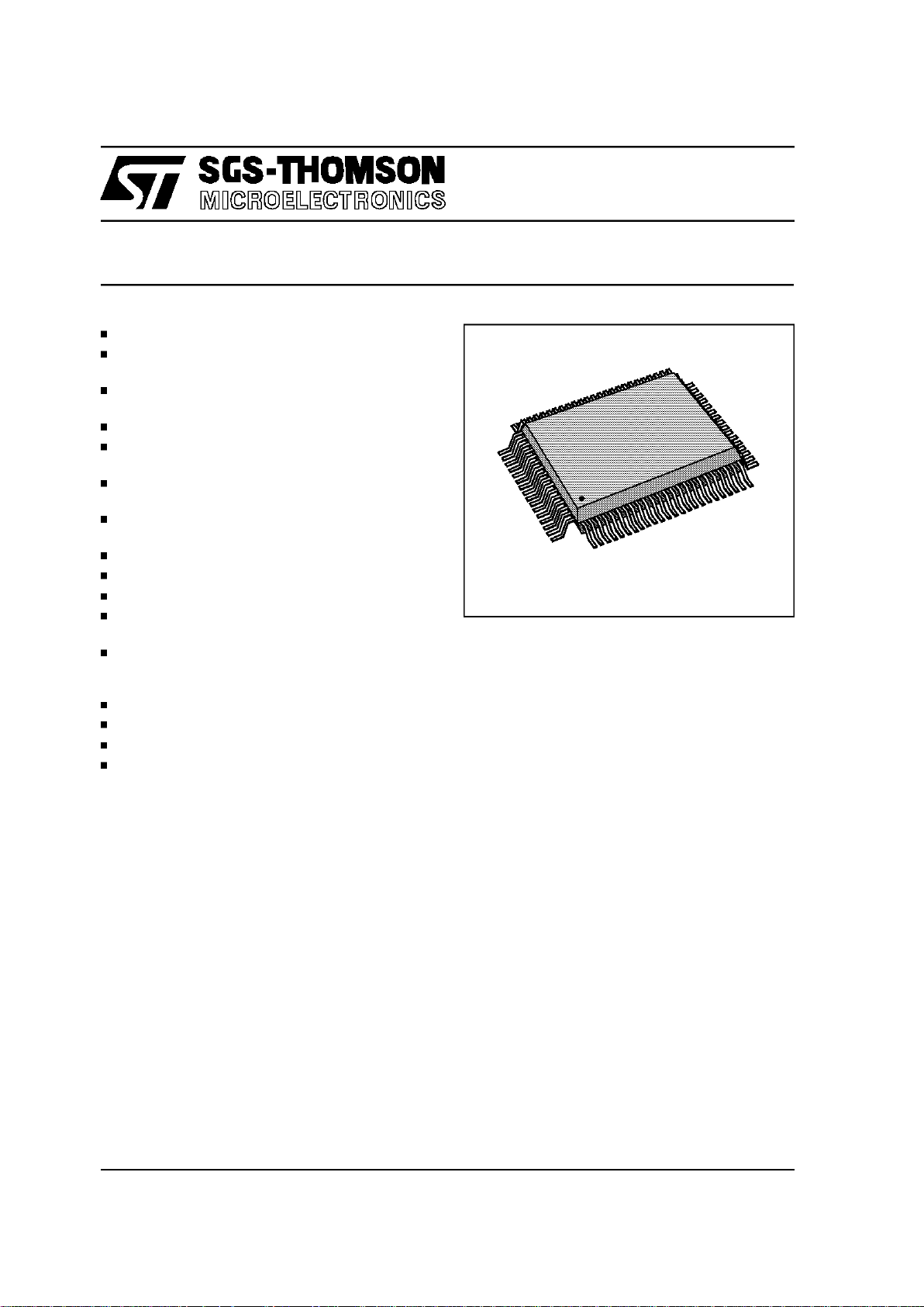
PQFP100
Single-chipcontroller for SERCOS interface
Real timecommunication for industrial control
systems
8/16-bitbus interface, Intel and Motorola con-
trol signals
Dual portRAMwith 1024 words * 16-bit
Data communicationsvia optical fiber rings, RS
485 rings and RS485 busses
Maximumtransmissionrateof 4 Mbaud with in-
ternal clock recovery
Maximumtransmissionrateof 10 Mbaud with
external clockrecovery
Internal repeater for ring connections
Full duplex operation
Modulationof power of optical transmitterdiode
Automatictransmissionof synchronous and
data telegrams in the communicationcycle
Flexible RAM configuration, communication
data stored in RAM (single or double buffer)or
transfervia DMA
Synchronizationby external signal
Timing control signals
Automaticservicechannel transmission
100-pin plasticflat-packcasing
1/30
Page 6
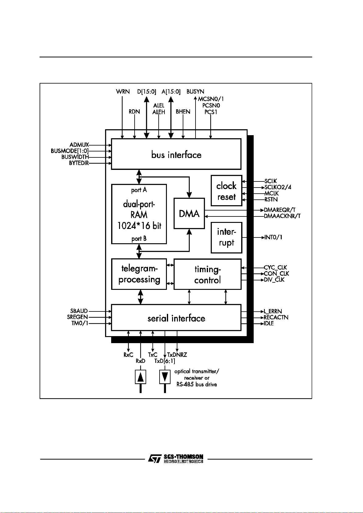
Figure1. SERCON410B Block Diagram
SERCON410B
2/30
Page 7

Figure2. SERCON410B Pin Configuration
SERCON410B
3/30
Page 8

Figure3. SERCOS Interface withRing Connection
Figure4. SERCON410B with RS-485 bus Connection
SERCON410B
4/30
Page 9

1 GENERALDESCRIPTION
The SERCOS interface controller SERCON410B
is anintegrated circuit forSERCOSinterface communication systems. The SERCOS interface is a
digital interface for communication between systems which have to exchange information cyclically at short, fixed intervals (65 µs to 65 ms).It is
appropriate for the synchronous operation of distributed control or test equipment (e.g. connection
between drivesand numeric control).
A SERCOS interfacecommunication system consists of one master and several slaves (Fig. 3).
These units are connected by a fiber optical ring.
This ring startsand ends at the master.The slaves
regenerate and repeat their received data or send
their owntelegrams. By this method the telegrams
sent by the master are received by all slaveswhile
the master receives data telegrams from the
slaves. The optical fiber assures a reliable highspeed datatransmission with excellent noise immunity.
The SERCOS interface controller contains all the
hardware-related functions of the SERCOS interface and considerably reduces thehardware
costs and the computing time requirements of the
microprocessor. It is the direct link between the
electro-opticalreceiver and transmitterand the microprocessorthat executes the control algorithms.
The SERCON410Bcanbeused bothfor SERCOS
interface mastersand slaves.
The circuitcontains the followingfunctions(Fig.1):
-
Interface to the microprocessor with a data
bus width of 8 or 16 bits and with control lines
according to Intel or Motorola standards.
-
A serial interface for making a direct connection with the optical receiver and transmitter of
the fiber optic ring or with drivers to an electric
ring or bus. Data and clock regeneration, the
repeater for ring topologies and the serial
transmitter and receiver are integrated. The
signals are monitored and test signals generated. The serial interface operates up to
4Mbaud without external circuitry and up to 10
Mbaud with external clock regeneration.
-
A dual port RAM (1024 * 16 bit) for control and
communication data. The organization of the
memoryis flexible.
-
Telegram processing for automatic transmission and monitoring of synchronous and data
telegrams. Only transmission data which is intended for the particular interface user is processed. The transmitted data is either stored in
the internal RAM (single or double buffer) or
transferred via direct memory access (DMA).
The transmission of service channel information over several communication cycles is executed automatically.
In addition to the SERCOS interface the SERCON410B can also be used for other real-time
communications tasks. As an alternative to the fiberoptical ring also bus topologies with RS-485
signals are supported (Fig. 4). The SERCON410B
is therefore suitable for a wide range of applications.
SERCON410B
5/30
Page 10

2 PIN DESCRIPTION
Signal (s) Pin (s) IO Function
D15-0
77-80,
82-85,
87-90,
92-95
I/O
Data bus:for 8-bit-widebus interfaces, data is writtento and read via D7-0,
for 16-bit-wide bus interfaces via D15-0. When ADMUX is 1, the address
which is storedin the address latchwith ALEL and ALEH isinput via D15-0.
A15-0
56-59,
61-64,
66-69,
71-74
I/O
Addressbus: when ADMUX is 0the pins are inputs, when ADMUXis 1, they
are outputsfor the addressstored with ALEL (A7-0)and ALEH(A15-8). In
the 8-bit bus mode, A0 distinguishes which byte is transmitted via
D7-0 (depends on BYTEDIR). In the 16-bit bus mode, data is tansferred via
D7-0 only when A0 is 0. A10-1 selects the words of the internal RAM; A61the controlregisters.
ALEL, ALEH 54, 53 I
Address latchenable, low and high, active high: they are only used when
ADMUX is 1. When ALEL/ALEH is 1, the signals go from the data bus to
the address bus, when ALEL/ALEH = 0, they store the address. When
ADMUX is 0, ALEL/ALEH have to be connected to V
DD
.
RDN 51 I
Read: for the Intel bus interface, data is read when RDN is 0. For the
Motorola bus interface, data is read or written to when RDN is 0
(BUSMODE1 = 0) or RDN is 1 (BUSMODE1 = 1).
WRN 52 I
Write: for the Intel bus interface, data is written to when WRN is 0. For the
Motorola bus interface, WRN selects read (WRN = 1) and write (WRN = 0)
operations of the data bus.
BHEN 75 I
Byte high enable, active low: in the 16-bit bus mode, data is transferred via
D15-8 when BHEN is 0.
MCSN0,
MCSN1
46,47 I
Memory chip select, active low: to access theinternal RAM MCSN0 and
MCSN1 must be 0.
PCSN0,
PCS1
48,49 I
Periphery chip select, active low (PCSN0) and active high (PCSN1): to
access the control registers PCSN0 must equal 0 and PCS1 must equal 1.
BUSYN 45 O
RAM busy, active low: becomes active if an access to an address of the
dual port RAM is performed simultaneously to an access to the same
memory location by the internal telegram processing.
DMAREQR 38 O
DMA request receive, active high: becomes active ifdata from the receive
FIFO can be read. At the beginning of the read operation of the last word of
the receive FIFO, DMAREQR becomes inactive.
DMAACKRN 40 I
DMA acknowledge receive, active low: when DMAACKRN is 0, the receive
FIFO is read, independent of the levels on A6-1 and the chip select signals.
DMAREQT 39 O
DMA request transmit, active high: becomes active when data can be
written to the transmit FIFO. DMAREQT becomes inactive again at the
beginning of the last write access to the transmit FIFO.
DMAREQTN 41 I
DMA acknowledge transmit, active low: when DMAACKTN is 0, the
transmit FIFO is written to when there isa bus writeaccess independent of
the levels on A6-1 and the chip select signals.
ADMUX 96 I
Address databus: when ADMUX is 0 A15-0 are the address inputs, when
ADMUX is 1 A15-0 are theoutputs ofthe address latch.
BUSMODE0,
BUSMODE1
97,98 I
Busmode: BUSMODE0= 0 turnson theIntelbusinterface(RDN= read,
WRN= write),BUSMODE0= 1 selects theMotorola interface (RDN= data
strobe, WRN= read/write). BUSMODE1selects the 0-activedata strobe
(BUSMODE1 = 0)or the1-activedata strobe(BUSMODE1= 1).
BUSWIDTH 99 I Buswidth:selectsthe 8-bit- (0)or the16-bit-wide interface(1).
Table 1. SERCON410B I/O Port FunctionSummary
SERCON410B
6/30
Page 11

PIN DESCRIPTION(Continued)
Signal (s) Pin (s) IO Function
BYTEDIR 100 I
Byte address sequence: when BYTEDIR is0, A0 = 0 addresses the lower
8 bits of a word (low byte first), when BYTEDIR is 1, the upper 8 bits of a
word are addressed (high byte first).
INT0, INT1 44,43 O
Interrupts, active low or active high. Interrupt sources and signal polarity
are programmable.
SREGEN 28 I
Internal regeneration. When SREGEN is 0, clock and data regeneration
are turnedoff. RxC and TxC are clock inputs. WhenSREGEN is 1, clock
and data regeneration are turned on. RxC and TxC output the internally
generated clocks.
SBAUD 29 I
Baud rate. When regeneration is turned on, SBAUD selects the baud rate
(f
SCLK/
16 whenSBAUD is 0, f
SCLK
/32 when SBAUD is 1). Can be
overwritten by the microprocessor.
RxD
14
I Receive data for the serial interface.
RxC
12
I/O
Receive clockfor the serialinterface. When regeneration is turned off
(SREGEN = 0), clock input for the serial receiver and transmitter (only
when repeater is turned on); when regeneration is turned on (SREGEN= 1)
output ofthe internally generated receive clock. Themaximum frequency
is 10 MHz.
RECACTN
26
O
Receive active,active low. Indicates that the serial receiver is receiving a
telegram.
TxD1
16
O Transmit data. The pin can be switched to a high impedance state.
TxD6-2
22,21,2
0,
18,17
O
Transmit data or output port. The pins either output the serial data or can
be used as parallel output ports. When they output transmit data, each pin
can be switched to a high impedance state individually.
TxDNRZ
24
O NRZ-coded transmit data.
TxC
13
I/O
Transmit clock for the serial interface. When regeneration is turned off
(SREGEN = 0) and the repeater is turned off,it is the clock input for the
serial transmitter; when regeneration is turned on (SREGEN = 1) itis the
output forthe internally generated transmit clock. The maximum frequency
is 10 MHz.
IDLE
25
O Transmitter active, active low. When transmitting own data IDLE is 0.
TM0, TM1
30,31
I
Turn on test generator: TM0 = 0 switches TxD1-6 to continuous signal light,
TM1 = 0 switch-over to zero bit stream. The processor can overwrite the
level of TM1-0.
L_ERRN
32
O
Line error, active low: goes low when signal distortion is too high or when
the receive signal is missing. The operating mode is programmed by the
processor.
CYC_CLK
34
I
SERCOS interface cycle clock: CYC_CLK synchronizes the
communication cycles.The polarity is programmable.
CON_CLK
35
O
Control clock: becomes active within a communication cycle. Time,
polarity and width are programmable.
DIV_CLK 36 O
Divided control clock: becomes active several times within a ommunication
cycle. Number of pulses, start time, repetition rate and polarity are
programmable, the pulse width is 1µs.
SCLK 2 I
Serial clock for clock regeneration: the frequency is 16 or 32 times the
baud rate, the maximum frequency is 64 MHz.
Table 1. SERCON410B I/O Port FunctionSummary
(Continued)
SERCON410B
7/30
Page 12

Signal (s) Pin (s) IO Function
SCLKO2 6 O Clock output: outputs the SCLK clock divided by 2.
SCLKO4 5 O Clock output: outputs the SCLK clock divided by 4.
MCLK 4 I
Master clock for telegram processing and timing control,frequency 12 to 20
MHz.
RSTN 10 I Reset, active low. Must be zerofor at least 50 ns after power on.
TEST 7 I Test, active high. Has to be tied to V
SS
.
OUTZ 11 I
Puts outputs into high impedance state, active high: OUTZ is 1 puts all pins
into a high impedance state. The clocks are turned off and the circuit is
reset. For the in-circuit test and for turning on the powerdown mode.
NDTRO 9 O
NAND treeoutput. For the test at the semiconductor manufacturers and for
the connection test after board production. NDTRO isnot set to a high
impedance state.
V
SS
3,15,23,
33,42,
50,60,
70,81,
91
Ground pins.
V
DD
1,8,19,
27,37,
55,65,
76,86
Power supply +5 V± 5%.
Table 1. SERCON410B I/O Port FunctionSummary
(Continued)
PIN DESCRIPTION(Continued)
SERCON410B
8/30
Page 13

3 ELECTRICALCHARACTERISTICS
3.1 ABSOLUTEMAXIMUM RATINGS
Symbol Parameter Value Unit
V
DD
Supply Voltage -0.3 to 7.0 V
V
I
Input Voltage VSS-0.3 to VDD+0.3 V
V
O
Output Voltage VSS-0.3 to VDD+0.3 V
T
STG
Storage Temperature -55 to +150 °C
3.2 RECOMMENDED OPERATINGCONDITIONS
Symbol Parameter
Value
Unit
Min. Max.
T
A
Operating Temperature -40 85 °C
V
DD
Operating SupplyVoltage 4.75 5.25 V
f
SCLK
Clock Frequency SCLK 64 MHz
f
MCLK
Clock Frequency MCLK 20 MHz
f
TxC,fRxC
Clock Frequency TxC, RxC 10 MHz
Symbol Parameter Test Conditions
Value
Unit
Min. Typ. Max.
V
IL
Input Low Level Voltage 0.8 V
V
IH
Input High Level Voltage
2.4 V
V
T+
Schmitt trig.+ve threshold All pins except
D15-0, A15-0,
ALEL, ALEH,
RDN, WRN,
BHEN, MCSN0-1,
PCSN0, PCS1,
DMAACKTN,
DMAACKRN
2.0 2.4 V
VT- Schmitt trig. +ve threshold 0.6 0.8 V
(VDD=5V± 5%TA= -40°C to +85°C,unlessotherwise specified)
3.3 DC ELECTRICALCHARACTERISTICS
SERCON410B
9/30
Page 14

Symbol Parameter Test Conditions
Value
Unit
Min. Typ. Max.
I
IL
Low Level Input Current
(Pull-up resistor)
VI = V
SS
-450 -50 -30 µA
I
IH
High Level Input Current
VI = V
DD
-10 <1 10 µA
V
OL
Low level Output Voltage,
allO- and I/O-pinsexceptTXD6-1
I
OI
=-4 mA 0.4 V
V
OH
High level output voltage,
allO- and I/O-pinsexceptTXD6-1
I
OH
=+4 mA 2.4 V
V
OL
Highleveloutputvoltage,
allO- and I/O-pinsexceptTXD6-1
I
OI
=-8 mA 0.4 V
V
OH
High level output voltage,
pins TXD6-1
IOH = +8 mA V
DD
- 0.5
I
OZ
Tri-state output leakage VO=0VorV
DD
-10 <1 +10 µA
I
KLU
I/O latch-up current V<VSSV>V
DD
200mA mA
V
ESD
Electrostatic protection C=100 pF, R = 1.5 k 2000 V
C
PIN
Pin capacitance 10 pF
DC ELECTRICALCHARACTERISTICS (Continued)
SERCON410B
10/30
Page 15

Figure5. Timing of Clock MCLK and Related Outputs
(C
load
=50pF,VDD=5V±5% TA=-40°C to +85 °C)
3.4 AC ELECTRICALCHARACTERISTICS
3.4.1 Clock InputMCLK
Symbol Parameter
Value
Unit
Min. Type Max.
f
MCLK
Clock Frequency MCLK 12 20 MHz
t
MCLK0
MCLK Low 20 ns
t
MCLK1
MCLK High 20 ns
t
MCLD
Output Delay Rising Edge MCLK to
DMAREQR/T, CON_CLK, DIV_CLK
30 ns
Figure6. Timing of Clock SCLK
3.4.2 Clock InputSCLK
Symbol Parameter
Value
Unit
Min. Type Max.
f
SCLK
Clock Frequency SCLK 64 MHz
t
SCLK0
SCLK Low 6.5 ns
t
SCLK1
SCLK High 6.5 ns
SERCON410B
11/30
Page 16

Figure7. Timing of SerialClock Inputs RxC and TxC and RelatedSignals
AC ELECTRICALCHARACTERISTICS (Continued)
3.4.3 SerialClock
Symbol Parameter
Value
Unit
Min. Type Max.
f
RTXC
Clock Frequency RxC, TxC 10 MHz
t
RTXC0
RxC, TxC Low 40 ns
t
RTXX1
RxC, TxC High 40 ns
t
RTOUT
Output Delay RxC, TxC toTxD6-1,
TxDNRZ, IDLE, RECACTN
45 ns
t
RXDSU
Setup RxD to Falling Edge of RxC 15 ns
(SREGEN= 0, external clock regeneration,RxC and TxC are inputs)
Figure8. Timing of SerialClock Inputs RxC and TxC and RelatedSignals
3.4.4 Address Latch
Symbol Parameter
Value
Unit
Min. Type Max.
t
ALEW
Pulse Width ALEL, ALEH 25 ns
t
ALESU
SetupTimeD15-0ToFalling EdgeALEH,
ALEL
10 ns
t
ALEHD
HoldTime Falling Edge ALEH,ALEL to D15-0 5 ns
t
DA
Delay from D15-0 to A15-0 20 ns
SERCON410B
12/30
Page 17

Figure9. Read Access of Control Registers
AC ELECTRICALCHARACTERISTICS (Continued)
3.4.5 ReadAccess of Control Registers
Symbol Parameter
Value
Unit
Min. Type Max.
t
ASU
Setup time A6-0, BHEN, PCSN0, PCS1,
DMAACKNR, WRN (only Motorola mode) to
fallingedge RDN (Intelor Motorolamode
with low active strobe) or rising edge RDN
(Motorola mode with high active strobe)
0ns
t
AHD
Holdtime A10-0, BHEN,MCSN0-1,WRN
(only Motorola mode) to rising edge RDN
(Intel Motorola mode with low active strobe)
or falling edge RDN (Motorola mode with high
activestrobe)
0ns
t
PAD
AccesstimeA6-0, BHEN,PCSN0,PCS1,
DMAACKNR, WRN(only Motorola mode)to
D15-0valid
50 ns
t
PRDD
Access time RDN to D15-0 valid 40 ns
t
RDZ
Delay RDN to D15-0 high-Z 15 ns
t
PRQ
Delay RDN to DMAREQR low 30 ns
SERCON410B
13/30
Page 18

Figure10. Read Access of Dual Port RAM
AC ELECTRICALCHARACTERISTICS (Continued)
3.4.6 ReadAccess of Dual Port RAM
Symbol Parameter
Value
Unit
Min. Type Max.
t
ASU
Setup time A10-0, BHEN, MCSN0-1, WRN
(only Motorola mode)to falling edge RDN
(Intel or Motorola mode with low active
strobe) or rising edge RDN (Motorola mode
with high active strobe)
0ns
t
AHD
Holdtime A10-0, BHEN,MCSN0-1,WRN
(only Motorola mode) to rising edge RDN
(Intel Motorola mode with low active strobe)
or falling edge RDN (Motorola mode with high
activestrobe)
0ns
t
MRDD
AccesstimeRDN to D15-0valid 60 ns
t
MBSY
Delay RDN to BUSYN low 35 ns
t
MBHD
Delay BUSYN high to D15-0 valid 30 ns
t
RDZ
Delay RDN to D15-0 high-Z 15 ns
t
RD1
RDN andWRN highafter endof readaccess 30 ns
SERCON410B
14/30
Page 19

Figure11. Write Access to Control Registers
AC ELECTRICALCHARACTERISTICS (Continued)
Symbol Parameter
Value
Unit
Min. Type Max.
t
ASU
Setup time A6-0, BHEN, PCSN0, PCS1,
DMAACKNT, WRN (only Motorola mode) to
falling edge WRN (Intel mode) or RDN
(Motorola mode, strobe active low) or rising
edge RDN (Motorola mode, strobe active
high)
0ns
t
AHD
Holdtime A6-0, BHEN,PCSN0,PCS1,
DMAACKNT, WRN (only Motorolamode) to
risingedgeWRN (Intelmode)or RDN
(Motorola mode, strobeactive low)or falling
edgeRDN (Motorolamode,strobe active
high)
0ns
t
PWRW
PulsewidthWRN (Intelmode)or RDN
(Motorola mode)
30 ns
t
DSU
Setup time D15-0 to end of write access 10 ns
t
DHD
Hold time D15-0 to end of write access 10 ns
t
PRQ
Delay WRN or RDN to DMAREQT low 30 ns
3.4.7 WriteAccess to Control Registers
SERCON410B
15/30
Page 20

Figure12. Write Access to DUAL PortRAM
AC ELECTRICALCHARACTERISTICS (Continued)
Symbol Parameter
Value
Unit
Min. Type Max.
t
ASU
Setup time A10-0, BHEN, MCSN0-1, WRN
(only Motorola mode) to falling edge of
WRN (Intelmode) orRDN (Motorola mode
with low active strobe) or rising edge RDN
(Motorola mode with high active strobe)
0ns
t
AHD
Holdtime A10-0, BHEN,MCSN0-1,WRN
(onlyMotorolamode)to rising edgeof WRN
(Intelmode)or RDN (Motorola mode withlow
activestrobe)or risingedge RDN (Motorola
mode with highactivestrobe)
0ns
t
MWRW
PulsewidthWRN or RDN 30 ns
t
DSU
Setup time D15-0 to end of write access 10 ns
t
DHD
Hold time D15-0 after endof writeaccess 10 ns
t
MBSY
Delay WRN or RDN (begin of write access)
to BUSYN low
35 ns
t
MBHWH
Setup time BUSYN high to end of write
access
30 ns
t
WR1
WRN and RDN high after end of write
access
40 ns
3.4.8 WriteAccess to Dual PortRAM
SERCON410B
16/30
Page 21

4 CONTROLREGISTERSAND RAM DATA
STRUCTURES
4.1 CONTROLREGISTERADDRESSES
The following table is an overview of the control
registers. The address is the word address which
is inputbyA6-1. To calculate the byte address,the
value has to be multipliedby two. The reset val-
ues of the control registers are shown in bold.
A6-1 Bit Name R/W Value Function
0H 0-15 VERSION R 2 Circuitcode (0002H)
1H
0 RSTFL R/W
0
1
Reset has not taken place
Reset has taken place
1 SWRST W
0
1
Do not reset
Reset by software
2 (Not used)
3 REPON R/W
0
1
Repeater turned off
Repeater turned on
4 SREGEN R Level at SREGEN pin
5 REGMODE R/W
0
1
Sampling at the middle of bit
Sampling according to SERCOS interface
specification
6 R/W
0
1
Baud rate = f
SCLK
/16
Baud rate= f
SCLK
/32
7 POLRXD R/W
0
1
“Light on” when RxD = 0
“Light on” when RxD = 1
8 PRESYNC R/W
0
1
No pre-frame sync word
Pre-frame sync word
9 POLTXD R/W
0
1
“Light on” when TxD = 0
“Light on” when TxD = 1
10 ENTSBAUD R/W
0
1
Baud rate selected by SWSBAUD pin
Baud rateselected by SWSBAUD control bit
11 SBAUD R Level at pin SBAUD
12 RXDNRZ R/W
0
1
Receive data is NRZI-coded
Receive data is NRZI-coded
13 WRSYNC R/W
Direct RAM write access
RAM write access internally synchronized
14 DMAMODE R/W
0
1
DMAREQR/DMAREQT are static signals
DMAREQR/DMAREQT are pulses
15 (Not used)
All control registers can be written to and read
(R/W),with the exceptionof the controlbits that
initiate an action (W).The status registers can
only be read (R). When control registers which
contain bits that are not usedor can only be read,
are writtento, these bits can be set to 0 or 1; they
are notevaluated internally. If control registers
are read with bits that are not used, these bitsare
set to 0.
SERCON410B
17/30
Page 22

CONTROLREGISTER ADDRESSES (Continued)
A6-1 Bit Name R/W Value Function
2H
0-5 ENTXD1-6 R/W
0
1
Pin TxDn has a highimpedance
Pin TxDn is outputting transmit data
6 TXDMODE R/W
0
1
TXDMODE
TxD2-6 is outputting ENTXD2-6
7-9 TMODE0-2 R/W
0-3
4,6
5
7
Test functionsare controlledvia TM0-1 pins
Continuous signal light
Zero bit stream
Normal operation
10-11 TM0-1 R 0 Level at TM0-1
12 RDIST R
0
1
Receive data normal
Receive data over distortion limit
13 FIBBR R
0
1
Filler signal ordata is received
No edges on receive data
14-15 LMODE0-1 R/W
0
1
2
3
L_ERRN active by FIBBR and RDIST
L_ERRN active by RDIST
L_ERRN active by FIBBR
L_ERRN is inactive
3H
0 INTFL0 R
0
1
Interrupt INT0 not active
Interrupt INT0 active
1 ENINT0 R/W
0
1
Interrupt INT0 disabled
Interrupt INT0 disabled
2 POLINT0 R/W
0
1
Interrupt INT0 1-active
Interrupt INT0 0-active
3 INTFL1 R
0
1
Interrupt INT1 not active
Interrupt INT1 active
4 ENINT1 R/W
0
1
Interrupt INT1 disabled
Interrupt INT1 enabled
5 POLINT1 R/W
0
1
Interrupt INT1 1-active
Interrupt INT1 0-active
6 COMACT R
0
1
No transmission block is processed
Transmission blockis processed
7 COMBLK R
0
1
Transmission block0 isprocessed
Transmission block1 isprocessed
8 ENTMT R/W
0
1
Do not send data telegrams
Send data telegrams
9 FLTMT R
0
1
Data telegram is not sent
Data telegram is sent
10 FLRWAIT R
0
1
Data telegram is not expected
Data telegram is expected
11 FLREC R
0
1
Data telegram is not received
Data telegram is received
SERCON410B
18/30
Page 23

CONTROLREGISTER ADDRESSES (Continued)
A6-1 Bit Name R/W Value Function
3H
12 DMAREQT R
0
1
DMA request of transmit FIFO inactive
DMA request of transmit FIFO active
13 DMAREQR R
0
1
DMA request of receive FIFO inactive
DMA request of receive FIFO active
14 IDLE R Level at IDLE pin
15 RECACTN R Level at RECACTN pin
4H
INT_n R
0
1
Interrupt event has not occurred
Interrupt flag active, interrupt event has occurred
CLR_INT_n W
0
1
Do not modify interrupt flag
Clear interrupt flag
0 INT_RDIST R/W Interrupt receive data distorted
1 INT_FIBBR R/W Interrupt no receive data
2 INT_COMBLK0 R/W Interrupt start transmission block 0
3 INT_COMBLK1 R/W Interrupt start transmission block 1
4 INT_COMEND R/W Interruptend of transmission block
5 INT_PHAS0 R/W Interrupt phase MST = 0.
6 INT_PHASERR R/W Interruptphase MST errored
7 INT_MSTEARLY R/W Interrupt communication cycle start too early
8 INT_MSTLATE R/W Interrupt communication cycle start too late
9 INT_MSTMISS R/W InterruptMST missingtwice
10 INT_TSTART R/W Interruptstart of transmit telegram
11 INT_TEND R/W Interrupt end of transmit telegram
12 INT_RWAIT R/W Interrupt start waiting for receive telegram
13 INT_RSTART R/W Interrupt start of receive telegram
14 INT_REND R/W Interrupt end of receive telegram
15 INT_RERR R/W Interrupt error of receive telegram
5H
0-7 INT_SC_0-7 R/W Interrupt service container
8 INT_RMISS R/W Interrupt receive telegram missing twice
9-12 INT_TIME0-3 R/W Interrupt time TINT0-3
13 INT_DIVCLK R/W Interrupt DIVCLKsignal
14 INT_PROGERR R/W Interrupt programming error
15 INT_NEWADR R/W Interruptaddress change
SERCON410B
19/30
Page 24

CONTROLREGISTER ADDRESSES (Continued)
A6-1 Bit Name R/W Value Function
6H 0-15 EN0_INT_n R/W
0
1
Interrupt flag does not activateINT0
Interrupt flag activates INT0
Bit assignmentsame as for address 4H
7H 0-15 EN0_INT_n R/W
0
1
Interrupt flag does not activateINT0
Interrupt flag activates INT0
Bit assignmentsame as for address 5H
8H 0-15 EN1_INT_n R/W
0
1
Interrupt flag does not activateINT1
Interrupt flag activates INT1
Bit assignmentsame as for address 4H
9H 0-15 EN1_INT_n R/W
0
1
Interrupt flag does not activateINT1
Interrupt flag activates INT1
Bit assignmentsame as for address 5H
OAH
0-7 PHAS0 R/W
Phase for MST transmit (master) or MST
receive (slave) (reset value = 0FFH)
8-15 PHAS1 R/W
Phase for MST receive (slave)
(reset value = 0FFH)
OBH
0-7 PHASREC R Phase information of received MST
8-15 RECADR R Address of receive telegram
0CH
0 MSTEN R/W
0
1
MST isnot transmitted or received
MST istransmitted orreceived (SERCOS
interface mode)
1 MSTMASTER R/W
0
1
Receive MST (SERCOS interface slave)
Transmit and receive MST (SERCOS
interface master)
2 COMBLK0 R/W
0
1
When phase = PHAS0 transmission block 0
is processed
When phase = PHAS0 transmission block 1
is processed
3 COMBLK1 R/W
0
1
When phase = PHAS1 transmission block 0
is processed
When phase = PHAS1 transmission block 1
is processed
4 CON_CLK R Level at CON_CLK pin
5 ENCONCLK R/W
0
1
CON_CLK pin doesn’t become active
CON_CLK pin becomes active from TINT0 to
TINT1
6 POLCONCLK R/W
0
1
Signal at CON_CLK is1-active
Signal at CON_CLK is0-active
7 CYC_CLK R Level at CYC_CLKpin
8 ENCYCCLK R/W
0
1
CYC_CLK pin does not trigger timing control
CYC_CLK pin triggers timing control after
TCYCSTART
SERCON410B
20/30
Page 25

CONTROLREGISTER ADDRESSES (Continued)
A6-1 Bit Name R/W Value Function
OCH
9 POLCYCCLK R/W
0
1
Timing control triggered by rising edge of
CYC_CLK
Timing control triggered by falling edge of
CYC_CLK
10 CYCSTART W
0
1
No function
Trigger timing control after TCYCSTART
(master)
11 RDTCNT W
0
1
Do not read TCNT
Load TCNT to TCNTRD
12-15 NCYC R/W
Number of communcation cycles triggered by
CYC_CLK or CYCSTART
0DH
0-7 HS_TIMEOUT R/W Handshake timeout for service channel
8-15 BUSY_TIMEOUT R/W BUSY timeout for service channel
0EH
0-4 MCLKDIV R/W
Predivider value: fMCLK/1 MHz - 1
(reset value = 19)
5-7 (Not used)
8-12 MCLKST R/W Initial value for predivider
13-15 (Not used)
0FH 0-15 TSCYC0 R/W
SERCOS interface cycle timein •s for
transmission block 0
10H 0-15 TSCYC1 R/W
SERCOS interface cycle timein •s für
transmission block 1
11H 0-15 TCYCDEL R
Time at which MST is received, ring delay
(master)
12H 0-15 TCNTLT R Stored value of TCNT time counter
13H 0-15 TCNTST R/W Initial value for TCNT time counter
14H 0-15 TCYCSTART R/W Delay in triggering timing control
15H 0-15 JTSCYC1 R/W Receive time window for MST 1
16H 0-15 JTSCYC2 R/W Receive time window for MST 2
17H 0-15
PROGERR_FL R Error flags
CLR_PROGERR_FL W Clear errorflags
18H 0-15 JTRDEL1 R/W Receive time window for data telegram 1
19H 0-15 JTRDEL2 R/W Receive time window for data telegram 2
1AH 0-15 TINT0 R/W
Time at which time interrupt 0 and first edge
of CON_CLK occur
1BH 0-15 TINT1 R/W
Time at which time interrupt 1 and second
edge of CON_CLK occur
SERCON410B
21/30
Page 26

CONTROLREGISTER ADDRESSES (Continued)
A6-1 Bit Name R/W Value Function
1CH 0-15 TINT2 R/W Time at which time interrupt 2 occurs
1DH 0-15 TINT3 R/W Time at which time interrupt 3 occurs
1EH 0-15 TDIVCLK R/W
Time at which the firstpulse of DIV_CLK
occurs
1FH 0-15 DTDIVCLK R/W DIV_CLK pulse distance
20H
0-7 NDIVCLK R/W
Number of DIV_CLK pulses within one
communication cycle(reset value =0)
8 POLDIVCLK R/W
0
1
Pulses from DIV_CLK are 1-active
Pulses from DIV_CLK are 0-active
9-15 (Not used)
21H
0-9 THTPT R
Internal RAM address of telegram header of
transmitted telegram
10-15 (Not used)
22H 0-15 THT R
Control word 0 of telegram header of
transmitted telegram
23H
0-9 THWPT R
Internal RAM address of telegram header of
a telegram which is expected
10-15 (Not used)
24H 0-15 THW R
Control word 0 of telegram header of
telegram which is expected
25H
0-9 THRPT R
Internal RAM address of telegram header of
received telegram
10 MSTTCHK R/W
0
1
MST receive time is not checked
MST receive time is checked
11 PHAS12 R/W
0
1
Normal operation
Operating mode for SERCOS interface
phase 1 and 2
12 FLMDTADR R/W
0
1
Address of receive telegram different
from expected value
Address of receive telegram equal to
expected value
13-15 (Not used)
26H 0-15 THR R
Control word 0 of telegram header of
received telegram
27H
0-15 RFIFO R Receive FIFO
0-15 TFIFO W Transmit FIFO
SERCON410B
22/30
Page 27

4.2 DATA STRUCTURES WITHIN THERAM
In thisRAMthe first eleven words have a fixed meaning.
A10-1 Contents
0-1 COMPT0-1: Start of transmission blocks 0-1
2-9 SCPT0-7: Address service containers 0-7
10 NMSTERR: Error counter MST
4.2.1 TelegramHeaders
A telegramheader for receive telegramcontains thefollowingfive control words:
INDEX Bit Name Function
0
0-7 ADR Telegram address
8 DMA
Data storage in the internal RAM (DMA = 0) or DMA transfer
(DMA = 1)
9 DBUF
Data in the RAM: single buffer (DBUF = 0) ordouble buffer (DBUF
=1)
10 VAL
For single buffering(DMA= 0,DBUF =0) orDMA transfer (DMA =1):
telegram data is invalid (VAL = 0) or valid (VAL = 1); for double
buffering (DMA = 0, DBUF = 1): data in buffer 0 (VAL = 0) or buffer
1 (VAL = 1) is valid. Modified by controller at beginning and end of
receive telegrams.
11 ACHK
Telegrams are received if the address isvalid (ACHK = 1) or
independent on the received address (ACHK = 0). The received
address is stored at ADR.
12 TCHK
The time of receiving is checked (TCHK = 1) or not checked
(TCHK = 0).
13 RERR
The last telegram was free of error (RERR = 0) or errored or not
received (RERR = 1).
14 0 Marker bitfor telegram header of receive telegram.
15 0 Marker bitfor telegram header.
1 0-15 TRT Time for the start of telegram in µs after end of MST.
2 0-15 TLEN Length of telegram in data words (not including address).
3
0-9 PT
Word address within the RAM of the next telegram header or the
end marker.
10-15 (Not used)
4 0-15 NERR Errorcounter
The restof the RAM can be divided into data structures as required.
SERCON410B
23/30
Page 28

A telegramheader for transmit telegram comprisesfour control words:
DATA STRUCTURES WITHIN THE RAM(Continued)
Index Bit Name Function
0
0-7 ADR Telegram address
8 DMA Data storagein the RAM (DMA = 0) or DMA transfer (DMA = 1).
9 DBUF Data in RAM: singlebuffer (DBUF = 0) or double buffer(DBUF = 1).
10 VAL
For double buffering (DMA= 0, DBUF =1): datain buffer0 (VAL= 0)
or buffer1 (VAL= 1) arevalid. Setby processor.
11-12 EN
Data telegram isnot to be transmitted (EN = 0), transmitted once
(EN = 1),continuously (EN =2) or transmittedonlyif the previously
received telegram contains theexpected address (EN =3) (PHAS12
=1 and FLMDTADR = 1). If EN is 1 the circuit sets EN to 0 after
the transmit telegram has been started.
13 (Not used)
14 1 Marker bitfor telegram header of transmit telegram.
15 0 Marker bitfor telegram header.
1 0-15 TRT Time for the start of telegram in •s after the end of MST.
2 0-15 TLEN Length of the telegram in data words (not including address).
3
0-9 PT Word address of thenext telegram header or the end marker.
10-15 (Not used)
SERCON410B
24/30
Page 29

DATA STRUCTURES WITHIN THE RAM(Continued)
4.2.2 DataContainers
A data containercomprises one or two 16-bit control words as well as a variable number of data
words. If the data is stored in the internal RAM
(DMA =0) and a single buffer isused (DBUF = 0),
the data container has one buffer. Using RAM
Index Bit Name Function
0
0-9 LEN Number of 16-bit data words of the data block.
10 SVFL Flag, whether data block uses service container (SVFL = 1).
11-13 NSV Number of service container, which is used (0 - 7).
14 SCMASTER
Processing of service container in slave mode (SCMASTER = 0)
or master mode (SCMASTER = 1).
15 LASTDC
Last data container of the telegram (1) or further data containers
follow (0).
1 0-15 POS
Position of the data block within the telegram in number of words.
The firstdata record of a telegram has POS = 0 (only in case of
receive telegrams).
Figure13. Structure of Data Containers
storage anddouble buffering(DBUF= 1),twodata
buffers are needed. In case of DMA transfer (DMA
= 1) the data container only comprises the control
words (Fig. 13). The structure of the two control
words depends on whether a telegram is transmitted or received:
SERCON410B
25/30
Page 30

DATA STRUCTURES WITHIN THE RAM(Continued)
4.2.3 EndMarker
The end marker comprisestwo 16-bit words:
Index Bit Name Function
0
0-13 (Not used)
14 1 Marker bitfor the end marker.
15 1 Marker bitfor the end marker.
1 0-15 TEND Time after end ofMST at which the last telegram hasended (in µs).
Figure14. Structure of Service Container
4.2.4 ServiceContainers
A servicecontainer contains5 control wordsand a buffer (BUFLENwords, max. length 255) (Fig. 14)
SERCON410B
26/30
Page 31

DATA STRUCTURES WITHIN THE RAM(Continued)
Index Bit Name Function
0
0 HS_MDT Handshake-bit in MDT
1 L/S_MDT Read/write in MDT
2 END_MDT End in MDT
3-5 ELEM_MDT Data element type in MDT
6 SETEND END_MDT is to be set
7 M_BUSY
Service container waits for interaction of
microprocessor (M_BUSY = 1)
8-9 NINFO_WRITE Number of info words in write buffer (1 to 4)
10-11 (Not used)
12 INT_ERR Slave reports error
13 INT_END_WRBUF End of write buffer is reached
14 INT_END_RDBUF End of read buffer is reached
15 (Not used)
1
0 HS_AT Handshake bit in AT
1 BUSY_AT Busy bit in AT
2 ERR_AT Error bit in AT
3 CMD_AT Command modification bit in AT
4-6 (Not used)
7 RECERR Last transmission was correct (0) or errorneous (1)
8-9 NINFO_READ Number of info words in read buffer (1 to 4)
10-15 (Not used)
2
0-7 WRDATPT Pointer topresent position in write buffer
8-15 WRDATLAST Pointer to last position in write buffer
3
0-7 RDDATPT Pointer to present position in read buffer
8-15 RDDATLAST Pointer to last position in read buffer
4
0-7 ERR_CNT Error counter
8 BUSY_CNT Errorcountsdifferences ofhandshake (0)orBUSYcycles (1)
9 INT_SC_ERR Interrupt due to protocol error
10 INT_HS_TIMEOUT Interrupt due to handshake timeout
11 INT_BUSY_TIMEOUT Interrupt BUSY timeout
12 INT_CMD Slave has set command modification bit
13-15 (Not used)
For master mode (SCMASTER = 1) the control words are coded as follows:
SERCON410B
27/30
Page 32

DATA STRUCTURES WITHIN THE RAM(Continued)
The coding of the five control wordsdepends on the mode of the service channel. Using the slavemode
(SCMASTER = 0) they have the following structure:
Index Bit Name Function
0
0 HS_AT Handshake bit in AT
1 BUSY_AT Busybitin AT,also waiting formicroprocessor interaction
2 ERR_AT Error bit in AT
3 Error bit in AT Command modification bit in AT
4-6 ELEM Data element of present transmission
7 L/S Read (0)/write(1) of present transmission
8-9 NINFO_WRITE Number of info words in write buffer (1 to 4)
10-11 (Not used)
12 INT_ELEM_CHANGE Master has modified data element or read/write
13 INT_END_WRBUF End of write buffer is reached
14 INT_END_RDBUF End of read buffer is reached
15 INT_END_MDT Master reports end via END_MDT-bit
1
0 HS_MDT Handshake bit in MDT
1 L/S_MDT Read/write in MDT
2 END_MDT End bit in MDT
3-5 ELEM_MDT Data element in MDT
6 (Not used)
7 RECERR Last transmission was correct (0) or errorneous (1)
8-9 NINFO_READ Number of info words in read buffer (1 to 4)
10-15 (Not used)
2
0-7 WRDATPT Pointer topresent position in write buffer
8-15 WRDATLAST Pointer to last position in write buffer
3
0-7 RDDATPT Pointer to present position in read buffer
8-15 RDDATLAST Pointer to last position in read buffer
4
0-8 (Not used)
9 INT_SC_ERR Interrupt due toprotocolerror
10-15 (Not used)
SERCON410B
28/30
Page 33

5 PACKAGE MECHANICAL DATA
Figure15. SERCON410B 100 Pin Plastic Quad Flat Pack Package
Dim. mm inches
Min Typ Max Min Typ Max
A 3.40 0.134
A2 2.55 2.80 3.05 0.100 0.110 0.120
D 23.65 23.90 24.15 0.931 0.941 0.951
D1 19.90 20.00 20.10 0.783 0.787 0.791
D3 18.85 0.742
E 17.65 17.90 18.15 0.695 0.705 0.715
E1 13.90 14.00 14.10 0.547 0.551 0.555
E3 12.35 0.486
e 0.65 0.026
Number ofPins
ND 30
NE 20
N 100
6 ADDITIONALSUPPORTAND TOOLS
6.1 SERCOSINTERFACE SPECIFICATION
The SERCOS interface specification is available
at:
FördergemeinschaftSERCOSinterface e.V.
Herseler Str. 31
D-50389 Wesseling
Tel. xx49-2236-1517
Fax. xx49-2236-1542
6.2 SOFTWAREAND BOARDS FOR THE
SERCON410B
Driver software SERCDRV
Master and slave routines forthe SERCON410B
Written in ANSI-C
Independentfrom operating systemand processor
Contains:
-
initialization
-
start-up of SERCOS interface (phases 0 - 4)
-
service channel transmission
Easy portable to many microprocessorsand hardware platforms
PC-AT boardSERCEB
16-bit ISA bus
Receiver and transmitter for fibre optics (SERCOS
interface standard)
SERCON410Band additionaltimerchip 82C54
Additional RS-485-signals for serial connection
and synchronization
Wire wrap area for extension
Add-on board SERCINT
Multiplexed 16-bit address/data-bus
Receiver and transmitter for fibre optics (SERCOS
interface standard)
SERCON410B
AdditionalRS-485-signals for serial connection
These software and boards areavailable at:
IAM GmbH
Vertrieb Systemtechnik
Richard-Wagner-Str.1
D-38106 Braunschweig
Tel. xx49-531-3802-0
Fax.xx49-531-3802-110
SERCON410B
29/30
Page 34

Information furnished is believed to be accurate and reliable. However, SGS-THOMSON Microelectronicsassumes no responsability for the
consequences ofuse ofsuch information nor for any infringement ofpatents or other rights of third parties which may resultfrom itsuse. No
license is granted by implicationor otherwise under any patent or patent rights of SGS-THOMSON Microelectronics.Specifications mentioned
in this publication are subject to change without notice. This publication supersedes and replaces all informationpreviously supplied.
SGS-THOMSON Microelectronics products are not authorized for use as critical components in life support devices or systems without the
express writtenapprovalof SGS-THOMSON Microelectronics.
1994 SGS-THOMSON Microelectronics - All rights reserved.
Purchase ofI
2
C Components bySGS-THOMSON Microelectronics conveys a license under the Philips I2C Patent.
Rights to use these components in an I
2
C system is granted provided thatthe systemconforms tothe I2C Standard
Specification as defined by Philips.
SGS-THOMSON Microelectronics Group ofCompanies
Australia - Brazil - France - Germany - Hong Kong -Italy - Japan - Korea - Malaysia - Malta - Morocco
The Netherlands - Singapore - Spain - Sweden - Switzerland -Taiwan - Thailand - United Kingdom- U.S.A.
NOTES:
SERCON410B
30/30
 Loading...