

Page 1
SEMiX653GB176HDs
SEMiX® 3s
Trench IGBT Modules
SEMiX653GB176HDs
Features
• Homogeneous Si
• Trench = Trenchgate technology
•V
• UL recognised file no. E63532
Typical Applications*
with positive temperature
CE(sat)
coefficient
Absolute Maximum Ratings
Symbol Conditions Values Unit
IGBT
V
I
C
I
Cnom
I
CRM
V
CES
GES
Tj= 150 °C
I
= 2xI
CRM
Cnom
T
=25°C
c
T
=80°C
c
1700 V
619 A
438 A
450 A
900 A
-20 ... 20 V
VCC= 1000 V
V
t
psc
T
j
GE
V
CES
≤ 20 V
≤ 1700 V
= 125 °C
T
j
10 µs
-55 ... 150 °C
Inverse diode
T
I
F
I
Fnom
I
FRM
I
FSM
T
Tj= 150 °C
I
= 2xI
FRM
Fnom
tp= 10 ms, sin 180°, Tj=25°C
j
=25°C
c
T
=80°C
c
545 A
365 A
450 A
900 A
2900 A
-40 ... 150 °C
Module
I
t(RMS)
T
stg
V
isol
AC sinus 50Hz, t = 1 min 4000 V
600 A
-40 ... 125 °C
• AC inverter drives
•UPS
• Electronic welders
Characteristics
Symbol Conditions min. typ. max. Unit
IGBT
V
CE(sat)
V
CE0
r
CE
V
GE(th)
I
CES
C
ies
C
oes
C
res
Q
R
Gint
t
d(on)
t
r
E
on
t
d(off)
t
f
E
off
R
th(j-c)
IC=450A
V
=15V
GE
chiplevel
VGE=15V
VGE=VCE, IC= 18 mA 5.2 5.8 6.4 V
VGE=0V
V
= 1700 V
CE
VCE=25V
V
=0V
GE
G
VGE=- 8 V...+ 15 V
Tj=25°C
VCC= 1200 V
I
=450A
C
=3.6Ω
R
G on
R
=3.6Ω
G off
per IGBT 0.054 K/W
T
=25°C
j
= 125 °C
T
j
Tj=25°C
T
= 125 °C
j
T
=25°C
j
T
= 125 °C
j
T
=25°C
j
T
= 125 °C
j
f=1MHz
f=1MHz
f=1MHz
T
= 125 °C
j
Tj= 125 °C
Tj= 125 °C
Tj= 125 °C
Tj= 125 °C
Tj= 125 °C
22.45V
2.45 2.9 V
11.2V
0.9 1.1 V
2.2 2.8 mΩ
3.4 4.0 mΩ
3mA
mA
39.6 nF
1.65 nF
1.31 nF
4200 nC
1.67 Ω
290 ns
90 ns
300 mJ
975 ns
190 ns
180 mJ
GB
© by SEMIKRON Rev. 1 – 24.06.2010 1
Page 2
SEMiX653GB176HDs
SEMiX® 3s
Trench IGBT Modules
SEMiX653GB176HDs
Features
• Homogeneous Si
• Trench = Trenchgate technology
•V
• UL recognised file no. E63532
Typical Applications*
• AC inverter drives
•UPS
• Electronic welders
with positive temperature
CE(sat)
coefficient
Characteristics
Symbol Conditions min. typ. max. Unit
Inverse diode
V
V
r
F
I
RRM
Q
E
R
= V
F
F0
rr
rr
th(j-c)
IF=450A
EC
V
=0V
GE
chip
IF=450A
di/dt
= 4200 A/µs
off
V
=-15V
GE
V
= 1200 V
CC
per diode 0.11 K/W
T
=25°C
j
= 125 °C
T
j
Tj=25°C
T
= 125 °C
j
Tj=25°C
T
= 125 °C
j
T
= 125 °C
j
Tj= 125 °C
Tj= 125 °C
1.7 1.90 V
1.7 1.9 V
0.9 1.1 1.3 V
0.7 0.9 1.1 V
1.3 1.3 1.3 mΩ
1.8 1.8 1.8 mΩ
380 A
130 µC
73 mJ
Module
L
CE
R
CC'+EE'
R
th(c-s)
M
s
M
t
=25°C
T
res., terminal-chip
C
T
= 125 °C
C
per module 0.04 K/W
to heat sink (M5) 3 5 Nm
to terminals (M6)
2.5 5 Nm
20 nH
0.7 mΩ
1mΩ
Nm
w 300 g
Temperatur Sensor
R
100
B
100/125
Tc=100°C (R25=5 kΩ) 493 ± 5% Ω
R
T[K];
(T)=R100
exp[B
100/125
(1/T-1/T
100
)];
3550
±2%
K
GB
2 Rev. 1 – 24.06.2010 © by SEMIKRON
Page 3
SEMiX653GB176HDs
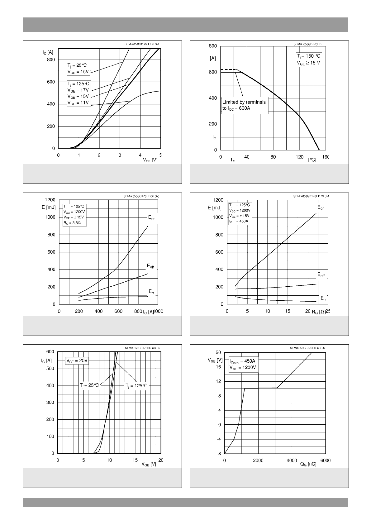
Fig. 1: Typ. output characteristic, inclusive R
Fig. 3: Typ. turn-on /-off energy = f (IC) Fig. 4: Typ. turn-on /-off energy = f (RG)
CC'+ EE'
Fig. 2: Rated current vs. temperature IC = f (TC)
Fig. 5: Typ. transfer characteristic Fig. 6: Typ. gate charge characteristic
© by SEMIKRON Rev. 1 – 24.06.2010 3
Page 4
SEMiX653GB176HDs
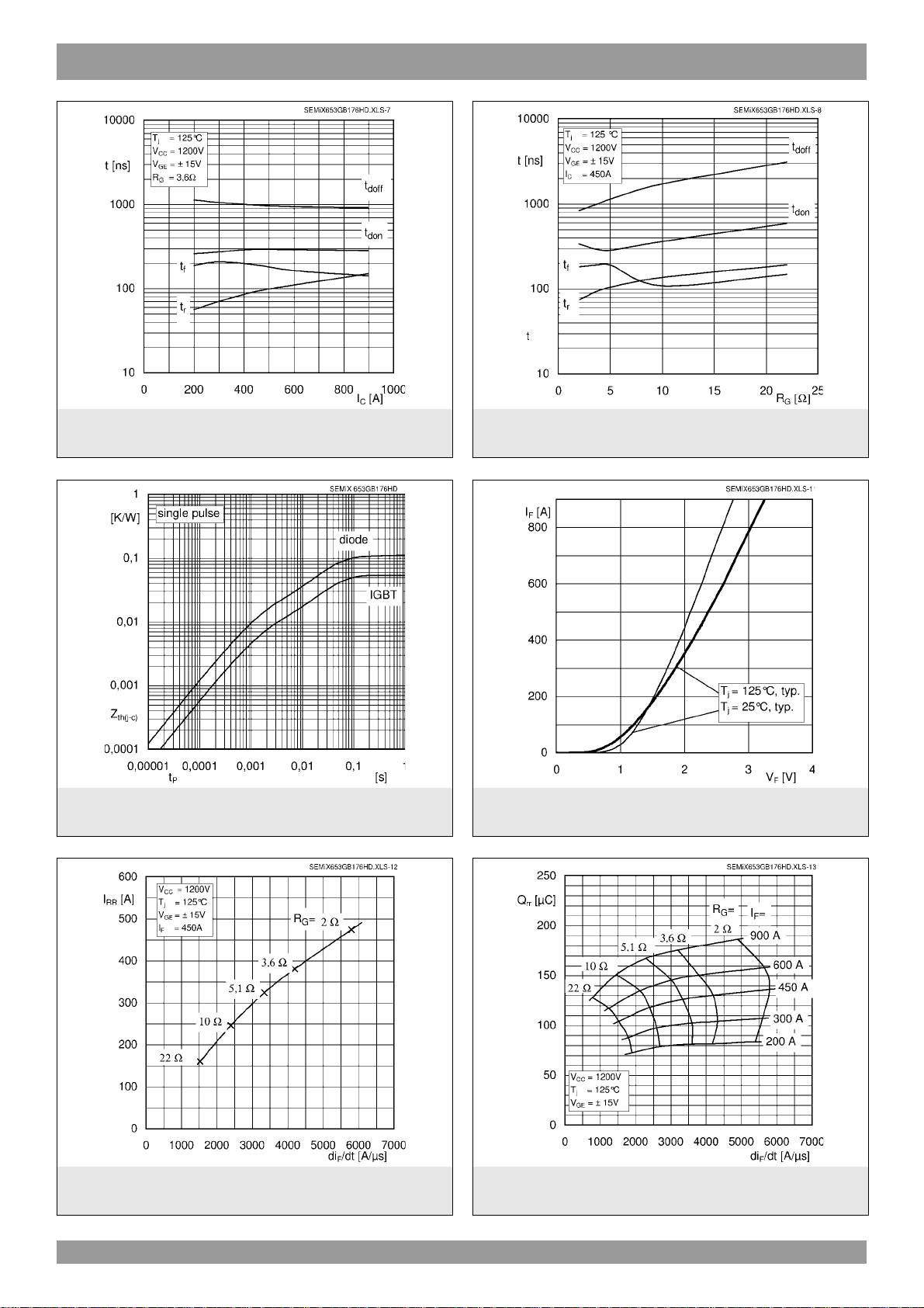
Fig. 7: Typ. switching times vs. I
C
Fig. 8: Typ. switching times vs. gate resistor R
G
Fig. 9: Typ. transient thermal impedance Fig. 10: Typ. CAL diode forward charact., incl. R
CC'+EE'
Fig. 11: Typ. CAL diode peak reverse recovery current Fig. 12: Typ. CAL diode recovery charge
4 Rev. 1 – 24.06.2010 © by SEMIKRON
Page 5
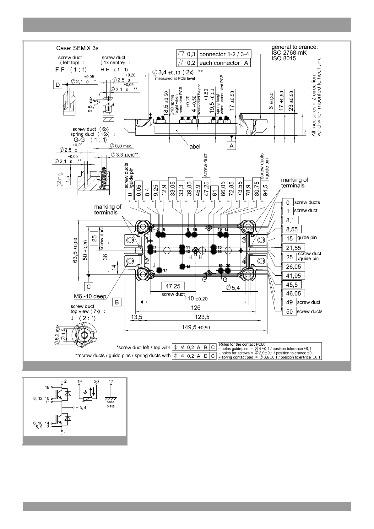
SEMiX653GB176HDs
SEMiX 3s
spring configuration
This is an electrostatic discharge sensitive device (ESDS), international standard IEC 60747-1, Chapter IX
* The specifications of our components may not be considered as an assurance of component characteristics. Components have to be tested
for the respective application. Adjustments may be necessary. The use of SEMIKRON products in life support appliances and systems is
subject to prior specification and written approval by SEMIKRON. We therefore strongly recommend prior consultation of our personal.
© by SEMIKRON Rev. 1 – 24.06.2010 5
 Loading...