

Page 1

S-MOS Systems, Inc. • 150 River Oaks Parkway • San Jose, CA 95134 • Tel: (408) 922-0200 • Fax: (408) 922-0238
371-1.0
1
SED1520/21
DOT MATRIX LCD DRIVER
S-MOS Systems, Inc.
October, 1996
Version 1.0 (Preliminary)
Page 2

–
S-MOS Systems, Inc. • 150 River Oaks Parkway • San Jose, CA 95134 • Tel: (408) 922-0200 • Fax: (408) 922-0238
371-1.0
2
THIS PAGE INTENTIONALLY BLANK
Page 3

S-MOS Systems, Inc. • 150 River Oaks Parkway • San Jose, CA 95134 • Tel: (408) 922-0200 • Fax: (408) 922-0238
371-1.0
3
Table of Contents
1.0 GENERAL DESCRIPTION . . . . . . . . . . . . . . . . . . . . . . . . . . . . . . . . . . . . . . . . . . . . . . . . . . . . . . . . . . . . . . . 5
1.1 Description . . . . . . . . . . . . . . . . . . . . . . . . . . . . . . . . . . . . . . . . . . . . . . . . . . . . . . . . . . . . . . . . . . . . . . 5
1.2 Features . . . . . . . . . . . . . . . . . . . . . . . . . . . . . . . . . . . . . . . . . . . . . . . . . . . . . . . . . . . . . . . . . . . . . . . . 5
1.3 SED1520 Family Specifications . . . . . . . . . . . . . . . . . . . . . . . . . . . . . . . . . . . . . . . . . . . . . . . . . . . . . . 6
1.4 Model Classification . . . . . . . . . . . . . . . . . . . . . . . . . . . . . . . . . . . . . . . . . . . . . . . . . . . . . . . . . . . . . . . 6
2.0 BLOCK DIAGRAMS . . . . . . . . . . . . . . . . . . . . . . . . . . . . . . . . . . . . . . . . . . . . . . . . . . . . . . . . . . . . . . . . . . . . 7
2.1 System Block Diagram . . . . . . . . . . . . . . . . . . . . . . . . . . . . . . . . . . . . . . . . . . . . . . . . . . . . . . . . . . . . . 7
2.2 Block Diagram . . . . . . . . . . . . . . . . . . . . . . . . . . . . . . . . . . . . . . . . . . . . . . . . . . . . . . . . . . . . . . . . . . . 8
2.3 Description of Circuit Blocks . . . . . . . . . . . . . . . . . . . . . . . . . . . . . . . . . . . . . . . . . . . . . . . . . . . . . . . . . 9
2.3.1 MPU Interface . . . . . . . . . . . . . . . . . . . . . . . . . . . . . . . . . . . . . . . . . . . . . . . . . . . . . . . . 9
2.3.2 Busy Flag . . . . . . . . . . . . . . . . . . . . . . . . . . . . . . . . . . . . . . . . . . . . . . . . . . . . . . . . . . . 11
2.3.3 Display Start Line Register . . . . . . . . . . . . . . . . . . . . . . . . . . . . . . . . . . . . . . . . . . . . . 11
2.3.4 Column Address Counter . . . . . . . . . . . . . . . . . . . . . . . . . . . . . . . . . . . . . . . . . . . . . . 11
2.3.5 Page Register . . . . . . . . . . . . . . . . . . . . . . . . . . . . . . . . . . . . . . . . . . . . . . . . . . . . . . . 11
2.3.6 Display Data RAM . . . . . . . . . . . . . . . . . . . . . . . . . . . . . . . . . . . . . . . . . . . . . . . . . . . . 11
2.3.7 Common Timing Generator . . . . . . . . . . . . . . . . . . . . . . . . . . . . . . . . . . . . . . . . . . . . . 12
2.3.8 Display Data Latch Circuit . . . . . . . . . . . . . . . . . . . . . . . . . . . . . . . . . . . . . . . . . . . . . . 12
2.3.9 LCD Driver Circuit . . . . . . . . . . . . . . . . . . . . . . . . . . . . . . . . . . . . . . . . . . . . . . . . . . . . 14
2.3.10 Display Timing Generator . . . . . . . . . . . . . . . . . . . . . . . . . . . . . . . . . . . . . . . . . . . . . . 14
2.3.11 Oscillation Circuit . . . . . . . . . . . . . . . . . . . . . . . . . . . . . . . . . . . . . . . . . . . . . . . . . . . . . 14
2.3.12 Reset Circuit . . . . . . . . . . . . . . . . . . . . . . . . . . . . . . . . . . . . . . . . . . . . . . . . . . . . . . . . 16
3.0 PIN CONFIGURATION . . . . . . . . . . . . . . . . . . . . . . . . . . . . . . . . . . . . . . . . . . . . . . . . . . . . . . . . . . . . . . . . . 19
3.1 Pin Configuration . . . . . . . . . . . . . . . . . . . . . . . . . . . . . . . . . . . . . . . . . . . . . . . . . . . . . . . . . . . . . . . . 19
3.2 Pin Description . . . . . . . . . . . . . . . . . . . . . . . . . . . . . . . . . . . . . . . . . . . . . . . . . . . . . . . . . . . . . . . . . . 20
3.2.1 Power Signals . . . . . . . . . . . . . . . . . . . . . . . . . . . . . . . . . . . . . . . . . . . . . . . . . . . . . . . 20
3.2.2 System Bus Interface Signals . . . . . . . . . . . . . . . . . . . . . . . . . . . . . . . . . . . . . . . . . . . 20
3.2.3 LCD Drive Circuit Signals . . . . . . . . . . . . . . . . . . . . . . . . . . . . . . . . . . . . . . . . . . . . . . 21
4.0 COMMANDS . . . . . . . . . . . . . . . . . . . . . . . . . . . . . . . . . . . . . . . . . . . . . . . . . . . . . . . . . . . . . . . . . . . . . . . . . 23
4.1 Display ON/OFF . . . . . . . . . . . . . . . . . . . . . . . . . . . . . . . . . . . . . . . . . . . . . . . . . . . . . . . . . . . . . . . . . 23
4.2 Display Start Line . . . . . . . . . . . . . . . . . . . . . . . . . . . . . . . . . . . . . . . . . . . . . . . . . . . . . . . . . . . . . . . . 23
4.3 Set Page Address . . . . . . . . . . . . . . . . . . . . . . . . . . . . . . . . . . . . . . . . . . . . . . . . . . . . . . . . . . . . . . . 24
4.4 Column Address . . . . . . . . . . . . . . . . . . . . . . . . . . . . . . . . . . . . . . . . . . . . . . . . . . . . . . . . . . . . . . . . . 24
4.5 Read Status. . . . . . . . . . . . . . . . . . . . . . . . . . . . . . . . . . . . . . . . . . . . . . . . . . . . . . . . . . . . . . . . . . . . . 25
4.6 Write Display Data . . . . . . . . . . . . . . . . . . . . . . . . . . . . . . . . . . . . . . . . . . . . . . . . . . . . . . . . . . . . . . . 25
4.7 Read Display Data . . . . . . . . . . . . . . . . . . . . . . . . . . . . . . . . . . . . . . . . . . . . . . . . . . . . . . . . . . . . . . . 26
4.8 Select ADC . . . . . . . . . . . . . . . . . . . . . . . . . . . . . . . . . . . . . . . . . . . . . . . . . . . . . . . . . . . . . . . . . . . . . 26
4.9 Static Drive ON/OFF . . . . . . . . . . . . . . . . . . . . . . . . . . . . . . . . . . . . . . . . . . . . . . . . . . . . . . . . . . . . . . 26
4.10 Select Duty . . . . . . . . . . . . . . . . . . . . . . . . . . . . . . . . . . . . . . . . . . . . . . . . . . . . . . . . . . . . . . . . . . . . . 27
Page 4

Table of Contents
S-MOS Systems, Inc. • 150 River Oaks Parkway • San Jose, CA 95134 • Tel: (408) 922-0200 • Fax: (408) 922-0238
371-1.0
4
4.11 Read Modify Write . . . . . . . . . . . . . . . . . . . . . . . . . . . . . . . . . . . . . . . . . . . . . . . . . . . . . . . . . . . . . . . 27
4.11.1 Cursor Blinking Sequence . . . . . . . . . . . . . . . . . . . . . . . . . . . . . . . . . . . . . . . . . . . . . 28
4.12 End . . . . . . . . . . . . . . . . . . . . . . . . . . . . . . . . . . . . . . . . . . . . . . . . . . . . . . . . . . . . . . . . . . . . . . . . . . 28
4.12.1 End Timing . . . . . . . . . . . . . . . . . . . . . . . . . . . . . . . . . . . . . . . . . . . . . . . . . . . . . . . . . 28
4.13 Reset . . . . . . . . . . . . . . . . . . . . . . . . . . . . . . . . . . . . . . . . . . . . . . . . . . . . . . . . . . . . . . . . . . . . . . . . . 29
4.14 Save Power (Combined Command) . . . . . . . . . . . . . . . . . . . . . . . . . . . . . . . . . . . . . . . . . . . . . . . . . 29
4.14.1 External Resistor Division Circuit . . . . . . . . . . . . . . . . . . . . . . . . . . . . . . . . . . . . . . . . 29
5.0 ELECTRICAL CHARACTERISTICS . . . . . . . . . . . . . . . . . . . . . . . . . . . . . . . . . . . . . . . . . . . . . . . . . . . . . . 31
5.1 Absolute Maximum Ratings . . . . . . . . . . . . . . . . . . . . . . . . . . . . . . . . . . . . . . . . . . . . . . . . . . . . . . . . 31
5.2 DC Characteristics . . . . . . . . . . . . . . . . . . . . . . . . . . . . . . . . . . . . . . . . . . . . . . . . . . . . . . . . . . . . . . . 32
5.3 Timing Characteristics . . . . . . . . . . . . . . . . . . . . . . . . . . . . . . . . . . . . . . . . . . . . . . . . . . . . . . . . . . . . 35
5.3.1 System Bus Read/Write I (80 Family MPU) . . . . . . . . . . . . . . . . . . . . . . . . . . . . . . . . 35
5.3.2 System Bus Read/Write II (68 Family MPU) . . . . . . . . . . . . . . . . . . . . . . . . . . . . . . . . 36
5.3.3 Display Control Timing. . . . . . . . . . . . . . . . . . . . . . . . . . . . . . . . . . . . . . . . . . . . . . . . . 37
6.0 MPU INTERFACE . . . . . . . . . . . . . . . . . . . . . . . . . . . . . . . . . . . . . . . . . . . . . . . . . . . . . . . . . . . . . . . . . . . . . 39
6.1 80 Family MPU . . . . . . . . . . . . . . . . . . . . . . . . . . . . . . . . . . . . . . . . . . . . . . . . . . . . . . . . . . . . . . . . . 39
6.2 68 Family MPU . . . . . . . . . . . . . . . . . . . . . . . . . . . . . . . . . . . . . . . . . . . . . . . . . . . . . . . . . . . . . . . . . 40
7.0 LCD DRIVER INTERCONNECTIONS . . . . . . . . . . . . . . . . . . . . . . . . . . . . . . . . . . . . . . . . . . . . . . . . . . . . . 41
7.1 SED1520FOA - SED1520FOA . . . . . . . . . . . . . . . . . . . . . . . . . . . . . . . . . . . . . . . . . . . . . . . . . . . . . 41
7.2 SED1520FAA - SED1520FAA . . . . . . . . . . . . . . . . . . . . . . . . . . . . . . . . . . . . . . . . . . . . . . . . . . . . . . 41
7.3 SED1520FOA - SED1521FOA *1 . . . . . . . . . . . . . . . . . . . . . . . . . . . . . . . . . . . . . . . . . . . . . . . . . . 41
7.4 SED1520FAA - SED1521FAA . . . . . . . . . . . . . . . . . . . . . . . . . . . . . . . . . . . . . . . . . . . . . . . . . . . . . . 42
7.5 HD44103CH - SED1521FAA . . . . . . . . . . . . . . . . . . . . . . . . . . . . . . . . . . . . . . . . . . . . . . . . . . . . . . . 42
8.0 TYPICAL CONNECTIONS WITH LCD PANEL . . . . . . . . . . . . . . . . . . . . . . . . . . . . . . . . . . . . . . . . . . . . . . 43
8.1 Duty 1/16, 10 characters x 2 lines . . . . . . . . . . . . . . . . . . . . . . . . . . . . . . . . . . . . . . . . . . . . . . . . . . . 43
8.2 Duty 1/16, 23 characters x 2 lines . . . . . . . . . . . . . . . . . . . . . . . . . . . . . . . . . . . . . . . . . . . . . . . . . . . 43
8.3 Duty 1/32, 33 characters x 4 lines . . . . . . . . . . . . . . . . . . . . . . . . . . . . . . . . . . . . . . . . . . . . . . . . . . . 44
8.4 Duty 1/32, 20 kanji characters x 2 lines . . . . . . . . . . . . . . . . . . . . . . . . . . . . . . . . . . . . . . . . . . . . . . . 44
8.5 Duty 1/32, 2–screen display, 20 kanji characters x 4 lines. . . . . . . . . . . . . . . . . . . . . . . . . . . . . . . . . 45
9.0 PACKAGE DIMENSIONS . . . . . . . . . . . . . . . . . . . . . . . . . . . . . . . . . . . . . . . . . . . . . . . . . . . . . . . . . . . . . . . 47
9.1 Plastic QFP 5-100 Pin . . . . . . . . . . . . . . . . . . . . . . . . . . . . . . . . . . . . . . . . . . . . . . . . . . . . . . . . . . . . 47
10.0 PAD LAYOUT . . . . . . . . . . . . . . . . . . . . . . . . . . . . . . . . . . . . . . . . . . . . . . . . . . . . . . . . . . . . . . . . . . . . . . . . 49
10.1 Pad Layout (SED1520D/SED1521D) . . . . . . . . . . . . . . . . . . . . . . . . . . . . . . . . . . . . . . . . . . . . . . . . 49
10.1.1 Al Pad . . . . . . . . . . . . . . . . . . . . . . . . . . . . . . . . . . . . . . . . . . . . . . . . . . . . . . . . . . . . . 50
10.1.2 Au Bump Pad . . . . . . . . . . . . . . . . . . . . . . . . . . . . . . . . . . . . . . . . . . . . . . . . . . . . . . . 50
10.2 Pad Coordinates (SED1520DAB) . . . . . . . . . . . . . . . . . . . . . . . . . . . . . . . . . . . . . . . . . . . . . . . . . . . 51
Page 5

S-MOS Systems, Inc. • 150 River Oaks Parkway • San Jose, CA 95134 • Tel: (408) 922-0200 • Fax: (408) 922-0238
371-1.0
5
1.0 General Description 1.0 – 1.2
1.0 GENERAL DESCRIPTION
1.1 DESCRIPTION
The SED1520 is a dot matrix LCD driver LSI intended for display of characters and graphics. The
bit-addressable display data, which is sent from a microcomputer, is stored in a built-in display data
RAM and generates the LCD drive signal.
The SED1520 incorporates innovative circuit design strategies to assure very low current dissipation and a wide range of operating voltages. With these features, the SED1520 permits the user to
implement high-performance handy systems operating from a miniature battery.
In order for the user to adaptively configure his system, the SED1520 family offers two application
forms. One form allows an LCD display of 12 characters
×
2 lines with an indicator with a single
chip. The other is dedicated to driving a total of 80 segments, enabling a medium-size display to
be achieved by using a minimum number of drivers.
1.2 FEATURES
•
Low-power CMOS technology
•
Fast CPU 8-bit data interface (80xx, 68xx)
•
Segment output . . . . . . . . . . 61 outputs
•
Common output . . . . . . . . . . 16 outputs
•
Duty cycle . . SED1520 . . . 1/16 to 1/32
SED1521 . . . 1/8 to 1/32
•
Built-in display data RAM. . . 2560 bits
•
Rich display command setting
•
On-chip CR oscillation circuit
•
Recommended expansion segment driver: 80 bit
•
Master/slave operation is supported
•
Low power consumption . . . 30 µ W
•
LCD voltage. . . . . . . . . . . . . 3.5 to 13V
•
Single power supply. . . . . . . 2.4 to 7.0V
•
Package. . . . . . . . . . . . . . . . QFP5-100 pin (F
OA
, F
AA
)
QFP15-100 pin (F
OC
, F
AC
)
Al pad (D
OA
, D
AA
)
Au bump (D
OB
, D
AB
)
TAB (T
OA
)
Page 6
1.3 – 1.4 1.0 General Description
S-MOS Systems, Inc. • 150 River Oaks Parkway • San Jose, CA 95134 • Tel: (408) 922-0200 • Fax: (408) 922-0238
371-1.0
6
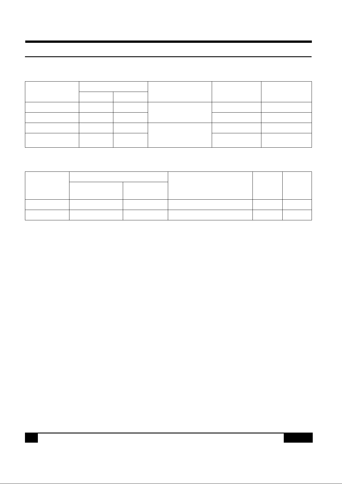
1.3 SED1520 FAMILY SPECIFICATIONS
1.4 MODEL CLASSIFICATION
Product Name
Clock Frequency
Applicable Driver
No. of SEG
Drivers
No. of COM
Drivers
On Chip External
SED1520F
OA
18kHz 18kHz
SED1520F
OA
,
SED1521F
OA
61 16
SED1521F
OA
— 18kHz 80 0
SED1520F
AA
— 2kHz SED1520F
AA
,
SED1521F
AA
,
HD44103CH
61 16
SED1521F
AA
— 2kHz 80 0
Model Name
Operating Clock
Connectable Drivers
SEG
Driver
COM
Driver
Internal
oscillator
External
clock
SED1520F
O*
18KHz 18KHz SED1520F
O*
, SED1521F
O*
61 ports 16 ports
SED1520F
A*
— 2KHz SED1520F
A*
, SED1521F
A*
61 ports 16 ports
Page 7
S-MOS Systems, Inc. • 150 River Oaks Parkway • San Jose, CA 95134 • Tel: (408) 922-0200 • Fax: (408) 922-0238
371-1.0
7
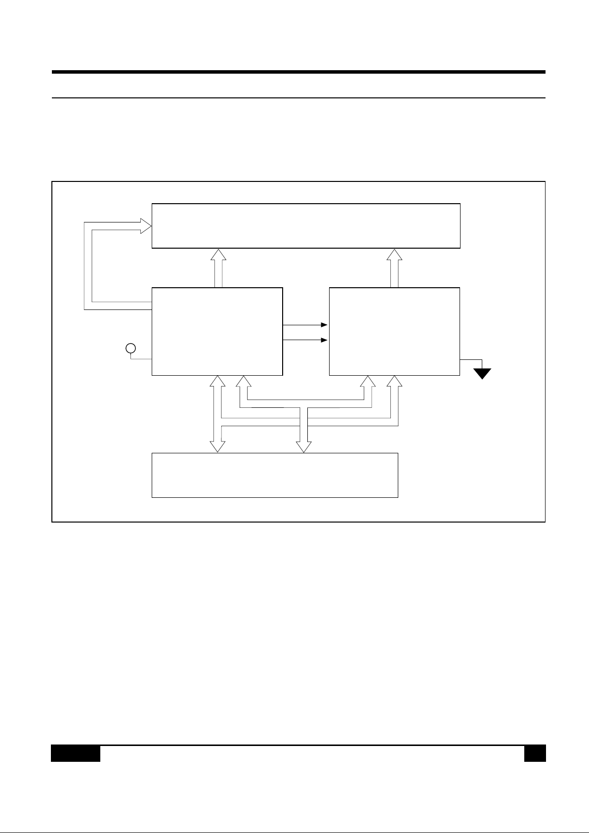
2.0 Block Diagrams 2.0 – 2.1
2.0 BLOCK DIAGRAMS
2.1 SYSTEM BLOCK DIAGRAM
SEG0~SEG60
28 CHAR × 2 LINES
CPU (68xx, 80xx)
SED1521SED1520
SEG0~SEG79
DATA
CONTROL
FR
Ck
M/S M/S
GND
V
DD
COM0~COM15
Page 8
2.2 – 2.2 2.0 Block Diagrams
S-MOS Systems, Inc. • 150 River Oaks Parkway • San Jose, CA 95134 • Tel: (408) 922-0200 • Fax: (408) 922-0238
371-1.0
8
2.2 BLOCK DIAGRAM
LINE ADDRESS DECODER
DISPLAY DATA RAM
2560 BITS
I/O BUFFER
INTERNAL BUS
LOW ADDRESS
REGISTER
BUS
HOLDER
LINE COUNTER
DISPLAY
TIMING
GENERATOR
DISPLAY START LINE REGISTER
FR
COMMAND
DECODER
COLUMN ADDRESS REGISTER
STATUS
MPU INTERFACE
COLUMN ADDRESS COUNTER
COLUMN ADDRESS DECODER
DISPLAY DATA LATCH CIRCUIT
LCD DRIVER CIRCUIT
COMMON
COUNTER
CL
(OSC2)
D
0
D
A
E , R/W
(OSC1)
RES
(RD)(WR)
0
, CS
7
∼
∼
V
DD
V
SS
V , V , M/S
1
V , V , V
235
(SG SG )
77 79
∼(SG SG )
61 76
∼ SG SG
060
∼CM CM
015
4
Page 9
S-MOS Systems, Inc. • 150 River Oaks Parkway • San Jose, CA 95134 • Tel: (408) 922-0200 • Fax: (408) 922-0238
371-1.0
9
2.0 Block Diagrams 2.3 – 2.3.1.3
2.3 DESCRIPTION OF CIRCUIT BLOCKS
2.3.1 MPU Interface
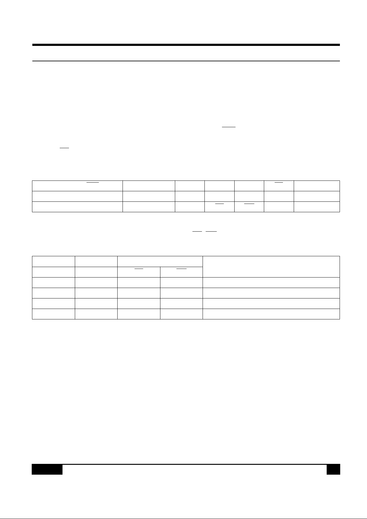
2.3.1.1 Selection of Interface Type
The SED1520 Series uses 8 bits of bi-directional data bus (D0–D7) to transfer data. The reset pin
is capable of selecting MPU interface; setting the polarity of RES
to either “H” or “L” can provide
direct interface of the SED1520 with a 68 or 80 family MPU (see Table 1 below).
With CS
at high level, the SED1520 is independent from the MPU bus and stays in standby mode.
In this mode, however, the reset signal is input independently of the internal status.
Table 1
2.3.1.2 Identification of Data Bus Signals
The SED1520 uses a combination of A0, E, R/W, (RD, WR) to identify a data bus signal.
Table 2
2.3.1.3 Access to Display Data RAM and Internal Register
In order to make matching of operating frequencies between the MPU and the display data RAM
or internal register, the SED1520 performs a sort of LSI–LSI pipelining via the bus holder attached
to the internal data bus.
Consider the case where the MPU reads the content of the display data RAM. In the first data read
cycle (dummy), the data is stored on the bus holder. In the next data read cycle, the data is read
from the bus holder to the system bus.
Also, consider the case where the MPU writes data to the display data RAM. In the first data write
cycle, the data is held on the bus holder. The data is written to the display data RAM before the
next data write cycle begins.
Polarity of RES
Type A0 E R/W CS D0–D7
“L” active 68 MPU
↑↑↑↑ ↑
“H” active 80 MPU
↑
RD WR
↑↑
Common 68 MPU 80 MPU
Function
A0 R/W RD
WR
1101Read display data
1010Write display data
0101Read status
0010Write to internal register (command)
Page 10
2.3.1.4 – 2.3.1.5 2.0 Block Diagrams
S-MOS Systems, Inc. • 150 River Oaks Parkway • San Jose, CA 95134 • Tel: (408) 922-0200 • Fax: (408) 922-0238
371-1.0
10
Therefore, MPU’s access to the SED1520 is affected not by display data RAM access time (t
ACC
,
t
DS
) but by cycle time (t
CYC
). This leads to faster transfer of data to and from the MPU. If the cycle
time requirement is not met, the MPU has only to execute the NOP instruction and this is apparently equivalent to execution of a waiting operation. However, there is a restriction on the read
sequence of the display data RAM; when an address is set, its data is output not to the first read
instruction (immediately following the address setting operation) but to the second read instruction.
Thus, one dummy read cycle is necessary after an address set or write cycle. This relation is
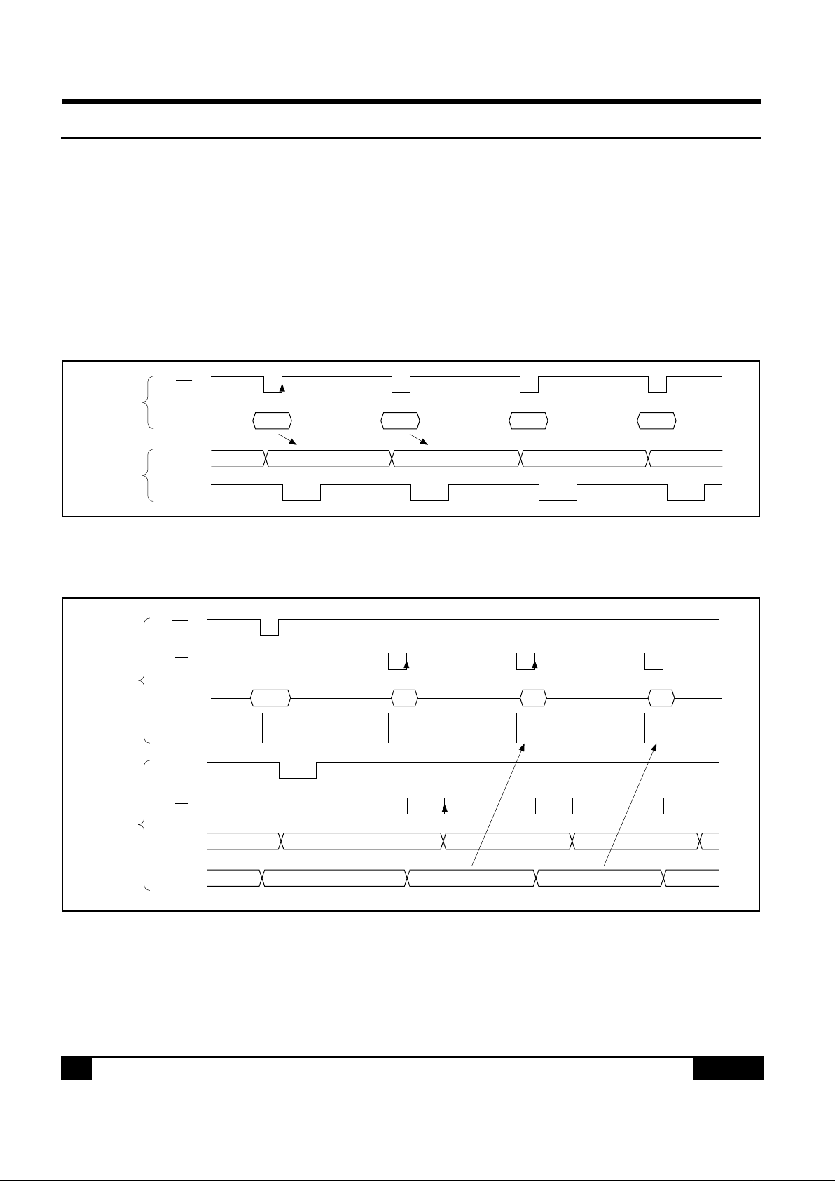
shown in Figures 2.3.1.4 and 2.3.1.5.
2.3.1.4 Write Timing Diagram
2.3.1.5 Read Timing Diagram
WR
DATA
MPU
Bus
Holder
WR
N N + 1 N + 2 N + 3
N + 2N + 1N N + 3
Internal
Timing
WR
DATA
MPU
Bus
Holder
Column
Address
WR
RD
RD
N
Address Set
at N
Dummy Read Data Read
at N
Data Read
at N+1
N n n+1
n + 1nN n + 2
N + 2N + 1N
Internal
Timing
Page 11

S-MOS Systems, Inc. • 150 River Oaks Parkway • San Jose, CA 95134 • Tel: (408) 922-0200 • Fax: (408) 922-0238
371-1.0
11
2.0 Block Diagrams 2.3.2 – 2.3.6
2.3.2 Busy Flag
Busy flag being “1” means that the SED1520 is performing its internal operation and any instruction
other than Read Status is disabled. The busy flag is output to pin D7 by a Read Status instruction.
As long as the cycle time (t
CYC
) requirement is met, the flag need not be checked before each com-
mand and this dramatically improves the MPU performance.
2.3.3 Display Start Line Register
This register is a pointer which determines the start line corresponding to COM0 (normally, the uppermost line of display) for display of data in the display data RAM. It is used for scrolling the display or changing the page from one to another. Executing the Set Display Start Line command
sets 5 bits of display start address in this register. Its content is preset in the line counter at each
timing the FR signal changes. The line counter is incremented synchronously to a CL input, thus
generating a line address for sequential reading of 80 bits of data from the display data RAM to the
LCD driver circuit.
2.3.4 Column Address Counter
The column address counter is a 7–bit presettable counter which gives column addresses of the
display data RAM as shown in Fig. 2.3.8.1. When a Read/Write Display Data command comes in,
the counter is incremented by 1. For any nonexisting address over 50H, the counter is locked and
not incremented.
The column address counter is independent from the page register.
2.3.5 Page Register
This register gives a page address of the display data RAM as shown in Fig. 2.3.8.1. The Set Page
Address command permits the MPU to access a new page of the display data RAM.
2.3.6 Display Data RAM
Dot data for display is stored in this RAM. Since the MPU and LCD driver circuit operate independently of each other, data can be changed asynchronously without adverse effect on the display.
One bit of the display data RAM is assigned to one bit of LCD:
LCD on = “1”
LCD off = “0”
The ADC command inverts the assignment relationship between a display data RAM column address and a segment output (see Fig. 2.3.8.1).
Page 12
2.3.7 – 2.3.8 2.0 Block Diagrams
S-MOS Systems, Inc. • 150 River Oaks Parkway • San Jose, CA 95134 • Tel: (408) 922-0200 • Fax: (408) 922-0238
371-1.012
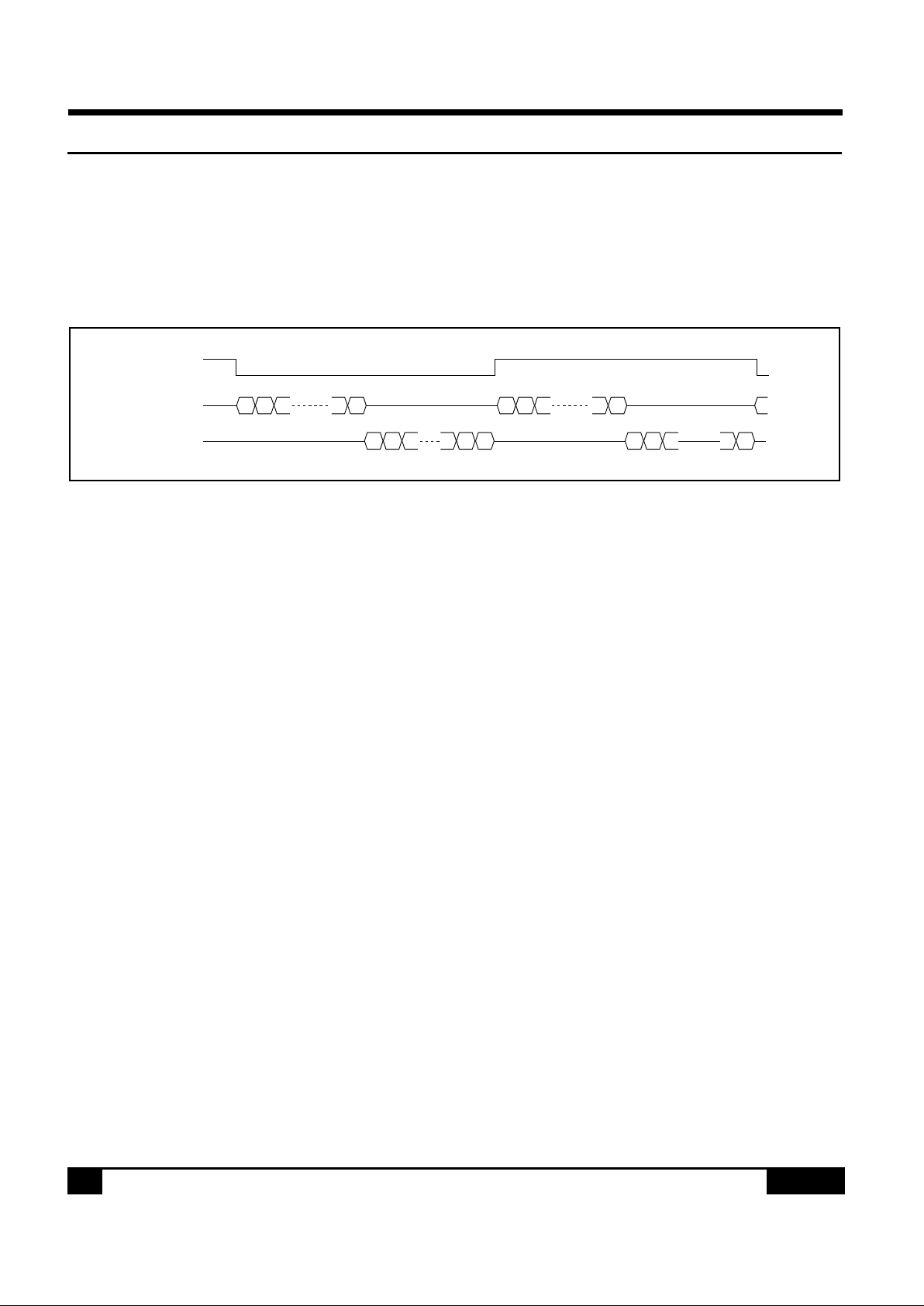
2.3.7 Common Timing Generator
This circuit generates common timing and frame (FR) signals from the basic clock (CL). The Select Duty command selects a duty of 1/16 or 1/32. The 1/32 duty is achieved by a two-chip (master
and slave) configuration (common multi-chip system).
2.3.7.1 Common Timing Diagram
2.3.8 Display Data Latch Circuit
The display data latch circuit temporarily stores the data which will be output from the display
data RAM to the LCD driver circuit at one-common intervals. The display ON/OFF and Static
Driver ON/OFF commands control the latched data so that the data in the display data RAM
remains unchanged.
0 1 21415 01 15
16 17 30 31 16 17 31
FR
(Master
Output)
Master
Common
Slave
Common
Page 13
S-MOS Systems, Inc. • 150 River Oaks Parkway • San Jose, CA 95134 • Tel: (408) 922-0200 • Fax: (408) 922-0238
371-1.0 13
2.0 Block Diagrams 2.3.8.1 – 2.3.8.1
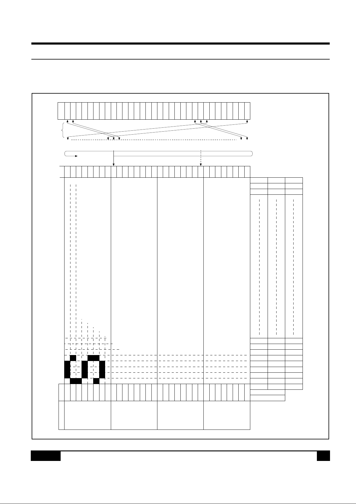
2.3.8.1 Relationship between Display Data RAM Locations and Addresses (Display Start
Line: 08)
Page Address
D1,D2=0,0
0,1
1,0
1,1
COM 0
123456789
101112131415161718192021222324252627282930
31
DATA
D
0
D1D2D3D4D5D6D7D0D1D2D3D4D5D6D7D0D1D2D3D4D5D6D7D0D1D2D3D4D5D6D7
Page 0
Page 1
Page 2
Page 3
(In this example,
the display start
line is set at
address 08.)
Start
1/16
Line
address
Associated
Line (ex.)
Assignment
Common
Output
00H
010203040506070809
0A
0B
0C
0D
0E
0F
101112131415161718
19
1A
1B
1C
1D
1E
1F
Column Address
ADC
Display Area
SEG Pin
SEG 0
1
2
3
4
5
6
7
D
0=“I”
4F
H
4E
4D
4C
4B
4A
49
48
D
0=“O”
00
H
01
02
03
04
05
06
07
77
78
79
02
01
00
4D
4E
4F
Page 14

2.3.9 – 2.3.11 2.0 Block Diagrams
S-MOS Systems, Inc. • 150 River Oaks Parkway • San Jose, CA 95134 • Tel: (408) 922-0200 • Fax: (408) 922-0238
371-1.014
2.3.9 LCD Driver Circuit
This circuit generates 80 sets of multiplexer that generate quartet levels for LCD driving. Display
data in the display data latch, common timing generator output and FR signal are combined to output an LCD driving waveform.
2.3.10 Display Timing Generator
This circuit generates an internal display timing signal from the basic clock (CL) and frame signal (FR).
The frame signal FR makes the LCD driver circuit generate a dual frame AC driving waveform
(type B) to drive LCD, while making both the line counter and common timing generator synchronized to the FR signal output LSI (dedicated common driver or the SED1520 master LSI). To
achieve these functions, the FR signal must be a clock with a duty of 50% which is synchronized
to the frame period.
The clock CL is a clock used to operate the line counter. For a system in which both the SED1520
and SED1521F coexist, they should be of LSI types having the same clock frequency to be applied
to pin CL.
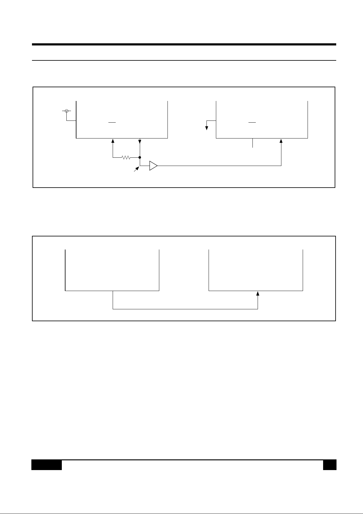
2.3.11 Oscillation Circuit
This circuit is a low-power CR oscillator which uses an oscillation resistor Rf alone to adjust the
oscillation frequency. It generates display timing signals. The SED1520 is available in two LSI
types if classified by oscillation: one LSI type contains an oscillation circuit and the other uses an
externally provided clock.
The oscillation resistor Rf is connected as shown below. Where an LSI containing an oscillation
circuit is operated with an external clock, it is necessary to input the clock with the same phase as
OSC2 of the master LSI to OSC2 of the slave LSI.
Page 15
S-MOS Systems, Inc. • 150 River Oaks Parkway • San Jose, CA 95134 • Tel: (408) 922-0200 • Fax: (408) 922-0238
371-1.0 15
2.0 Block Diagrams 2.3.11.1 – 2.3.11.2
2.3.11.1 LSI Containing Oscillator
* As the parasitic capacitance in this portion increases, the oscillation frequency will shift to a lower level. The Rf must
have a smaller value than the specification.
* For a system having two or more slave LSIs, a CMOS buffer is necessary.
2.3.11.2 LSI Operating with External Clock
Master LSI
(CS)
OSC1
M/S
VDD
VSS
(CL)
OSC2
R
f
*1
*2
( )
Slave LSI
(CS)
OSC1
Open
M/S
(CL)
OSC2
Y-Driver
CL2
SED1521F
AA
CL
Page 16

2.3.12 – 2.3.12 2.0 Block Diagrams
S-MOS Systems, Inc. • 150 River Oaks Parkway • San Jose, CA 95134 • Tel: (408) 922-0200 • Fax: (408) 922-0238
371-1.016
2.3.12 Reset Circuit
This circuit senses the leading edge or trailing edge of RES and initializes the system when its
power is switched on.
Initialization:
(a) Display off
(b) Display start line register: First line
(c) Static drive off
(d) Column address counter: Address 0
(e) Page address register: Page 0
(f) Select duty: 1/32
(g) Select ADC: Forward (ADC command D0 = “0”, ADC status flag = “1”)
(h) Read modify write off
The input at pin RES
is level-sensed to select an MPU interface mode as shown in Table 1. For
interfacing with an 80 family MPU, an “H” active reset signal is input to pin RES
. For interfacing
with a 68 family MPU, an “L” active reset signal is input to the pin. (See Fig. 7.)?????
As exemplified in section 6 “MPU Interface”, pin RES
is connected to the MPU reset pin. Thus the
SED1520 and the MPU are initialized at the same time. If system is initialized by pin RES
at power-
on, it may no longer be reset.
The Reset command causes initialization (b), (d) and (e).
Page 17

S-MOS Systems, Inc. • 150 River Oaks Parkway • San Jose, CA 95134 • Tel: (408) 922-0200 • Fax: (408) 922-0238
371-1.0 17
2.0 Block Diagrams 2.3.12.1 – 2.3.12.1
2.3.12.1 Example of LCD Driving Waveform
8
9
10
11
12
13
14
15
COM 0
1
2
3
4
5
6
7
FR
V
DD
V
SS
V
DD
V
1
V
2
V
3
V
4
V
5
V
DD
V
1
V
2
V
3
V
4
V
5
V
DD
V
1
V
2
V
3
V
4
V
5
V
DD
V
1
V
2
V
3
V
4
V
5
V
DD
V
1
V
2
V
3
V
4
V
5
V
5
V
4
V
3
V
2
V
1
V
DD
–V
1
–V
2
–V
3
–V
4
–V
5
V
5
V
4
V
3
V
2
V
1
V
DD
–V
1
–V
2
–V
3
–V
4
–V
5
COM0
COM1
COM2
SEG0
SEG1
COM0~SEG0
COM0~SEG1
SEG 0
123
4
0123 310123 31
0
1/6 bias, 1/32 duty
1/5 bias, 1/16 duty 1 2 3 15 0123 15
Page 18

2.3.12.1 – 2.3.12.1 2.0 Block Diagrams
S-MOS Systems, Inc. • 150 River Oaks Parkway • San Jose, CA 95134 • Tel: (408) 922-0200 • Fax: (408) 922-0238
371-1.018
THIS PAGE INTENTIONALLY BLANK
Page 19

S-MOS Systems, Inc. • 150 River Oaks Parkway • San Jose, CA 95134 • Tel: (408) 922-0200 • Fax: (408) 922-0238
371-1.0 19
3.0 Pin Configuration 3.0 – 3.1
3.0 PIN CONFIGURATION
3.1 PIN CONFIGURATION
Index
80
SEG22
SEG23
SEG24
SEG25
SEG26
SEG27
SEG28
SEG29
SEG30
SEG31
SEG32
SEG33
SEG34
SEG35
SEG36
SEG37
SEG38
SEG39
SEG40
SEG41
1
100
DB2
DB3
DB4
DB5
DB6
DB7
V
DD
RES
FR
V5
V3
V2
M/5
V4
V1
COM0
COM1
COM2
COM3
COM4
COM5
COM6
COM7
COM8
COM9
COM10
COM11
COM12
COM13
COM14
COM15
SEG60
SEG59
SEG58
SEG57
SEG56
SEG55
SEG54
SEG53
SEG52
SEG51
SEG50
SEG49
SEG48
SEG47
SEG46
SEG45
SEG44
SEG43
SEG42
DB1
DB0
V
SS
R/W(WR)
E(RD)
CL(OSC2)
CS(OSC1)
AO
SEG0
SEG1
SEG2
SEG3
SEG4
SEG5
SEG6
SEG7
SEG8
SEG9
SEG10
SEG11
SEG12
SEG13
SEG14
SEG15
SEG16
SEG17
SEG18
SEG19
SEG20
SEG21
70 60
50
40
30
10 20
90
SED1520/SED1521
75
5
65
15
55
25
85
45
95
35
Page 20

3.2 – 3.2.2 3.0 Pin Configuration
S-MOS Systems, Inc. • 150 River Oaks Parkway • San Jose, CA 95134 • Tel: (408) 922-0200 • Fax: (408) 922-0238
371-1.020
3.2 PIN DESCRIPTION
* Master LSI common outputs COM0–COM15 correspond to slave LSI outputs COM31–COM16.
3.2.1 Power Signals
VDD Connected to +5V power. Common to MPU power pin VCC.
V
SS 0V, connected to system GND.
V
1–V5 Multi-level power used to drive LCDs. Voltage specified to each LCD cell is divided by
resistors or impedance-converted by an operational amplifier before being applied. Each
voltage to be applied must be based on V
DD, while fulfilling the following conditions:
V
DD ≥ V1 ≥ V2 ≥ V3 ≥ V4 ≥ V5
3.2.2 System Bus Interface Signals
D7–D0 8–bit, tri-state, bi-directional I/O bus. Normally, connected to the data bus of an 8–/16–
bit standard microcomputer.
A0 Input pin. Normally, the LSB of the MPU address bus is connected to this input pin to
provide data/command selection.
0: Display control data on D
7–D0
1: Display data on D7–D0
RES Input pin. The SED1520 can be reset or initialized by setting RES to low level (if it is
interfaced with a 68 family MPU) or high level (if with an 80 family MPU). This reset operation occurs when an edge of the RES
signal is sensed. The level input selects the
type of interface with the 68 or 80 family MPU:
High level: Interface with 68 family MPU
Low level: Interface with 80 family MPU
Product name
Pin No.
74 75 96~100, 1~11 93 94 95
SED1520FOA OSC1 OSC2 COM0~COM15* M/S V4 V1
SED1521FOA CS CL SEG76~SEG61 SEG79 SEG78 SEG77
SED1520FAA CS CL COM0~COM15* M/S V4 V1
SED1521FAA CS CL SEG76~SEG61 SEG79 SEG78 SEG77
Page 21

S-MOS Systems, Inc. • 150 River Oaks Parkway • San Jose, CA 95134 • Tel: (408) 922-0200 • Fax: (408) 922-0238
371-1.0 21
3.0 Pin Configuration 3.2.3 – 3.2.3
CS Chip Select input signal which is normally obtained by decoding an address bus sig-
nal. Effective with “L” active and a chip operating with external clocks. For a chip containing an oscillator, CS
works as an oscillation amplifier input pin to which an
oscillation resistor (Rf) is connected. In this case, RD
, WR and E must be a signal
ANDed with CS.
E(RD
) Chip interfaced with 68 family MPU:
Enable Clock signal input for the 68 family MPU.
Chip interfaced with 80 family MPU:
“L” Active input pin to which the 80 family MPU RD
signal is connected.
With this signal held at “L”, the SED1520 data bus works as output.
R/W (WR
) Chip interface with 68 family MPU:
Read/Write control signal input pin.
R/W = “H” : Read
R/W = “L” : Write
Chip interfaced with 80 family MPU:
“L” Active input pin to which the 80 family WR
is connected. The signal
on the data bus is fetched by the leading edge of WR
.
3.2.3 LCD Drive Circuit Signals
CL Input signal effective with a chip using external clocks. This display data latch signal
increments the line counter (at the trailing edge) or the common counter (at the leading edge). CL is connected to CL2 of the common driver. For a chip containing an
oscillator, this pin works as the oscillation amplifier output pin to which an oscillation
resistor (Rf) is connected.
FR LCD AC signal I/O pin. Connected to pin M of the common driver.
I/O selection:
Chip containing commons M/S = 1 : Output
M/S = 0 : Input
Chip containing segments alone : Input
Page 22

3.2.3.1 – 3.2.3.2 3.0 Pin Configuration
S-MOS Systems, Inc. • 150 River Oaks Parkway • San Jose, CA 95134 • Tel: (408) 922-0200 • Fax: (408) 922-0238
371-1.022
SEG0– LCD column (segment) driving output. One of the VDD, V2, V3 and V5 levels is
SEG79 selected by a combination of the content of display RAM and the FR signal.
3.2.3.1 LCD Column (Segment) Driving Output Timing
COM0– LCD common (row) driving output. One of the VDD, V1, V4 and V5 levels is
COM15 selected by a combination of the output of the common counter and the FR
(COM31– signal. The common (row) scanning order for the slave LSI is reverse to that for
COM16) the master LSI.
3.2.3.2 LCD common (row) driving output
M/S Input signal which selects the master or slave LSI. Connected to VDD or VSS.
(SEG79)
M/S = V
DD: Master
M/S = V
SS : Slave
M/S selection changes the function of pins FR, COM0–COM15, OSC1 (CS
) and
OSC2 (CL):
The common scanning order for the slave driver is reverse to that for master.
M/S FR COM output OSC1 OSC2
VDD Output COM0–COM15 Input Output
VSS Input COM31–COM16 NC Input
FR
DATA
1
1
V
DD
V
2
V
5
V
3
0
0
10
Output Level
FR
Counter Output
1
1
V
S
V
1
V
DD
V
4
0
0
10
Output Level
Page 23

S-MOS Systems, Inc. • 150 River Oaks Parkway • San Jose, CA 95134 • Tel: (408) 922-0200 • Fax: (408) 922-0238
371-1.0 23
4.0 Commands 4.0 – 4.2
4.0 COMMANDS
Table 3 lists the commands used with the SED1520. This LSI uses a combination of A0, R/W (RD,
WR
) to identify a data bus signal. Interpretation and execution of a command depends not on external clock but on internal timing alone. Therefore, a command can be executed so fast that no
busy check is needed.
A detailed description of commands follows.
4.1 DISPLAY ON/OFF
This command forces all display to turn on or off.
D 0 = Display OFF
1 = Display ON
4.2 DISPLAY START LINE
This command specifies a line address (shown in Fig. 2.3.8.1) thus marking the display line that
corresponds to COM0. Display begins with the specified line address and covers as many lines as match
the display duty in address ascending order. Dynamic line address change with the Display Start Line
command enables column-wise scrolling or page change.
– High-order bits
R/W
A0 RD WR D7 D0
0101010111D
R/W
A0 RD WR D7 D0
010110A4A3A2A1A0
A4 A3 A2 A1 A0 Line address
00000 0
00001 1
——
——
11111 31
Page 24

4.3 – 4.4 4.0 Commands
S-MOS Systems, Inc. • 150 River Oaks Parkway • San Jose, CA 95134 • Tel: (408) 922-0200 • Fax: (408) 922-0238
371-1.024
4.3 SET PAGE ADDRESS
This command is used to specify a page address equivalent to a row address for MPU access to
the display data RAM. A required bit of the display data RAM can be accessed by specifying its
page address and column address. Changing the page address causes no change in display.
4.4 COLUMN ADDRESS
This command specifies a display data RAM column address. The column address is incremented
by 1 each time the MPU accesses from the set address to the display data RAM. Thus, it is possible for the MPU to gain continuous access to only the data. This incrementing stops with address
80; the page address is not continuously changed.
R/W
A0 RD WR D7 D0
010101110A1A0
A1 A0 Page
00 0
01 1
10 2
11 3
R/W
A0 RD WR D7 D0
0100A6A5A4A3A2A1A0
A6 A5 A4 A3 A2 A1 A0 Column address
0000000 0
0000001 1
——
——
1001111 79
Page 25

S-MOS Systems, Inc. • 150 River Oaks Parkway • San Jose, CA 95134 • Tel: (408) 922-0200 • Fax: (408) 922-0238
371-1.0 25
4.0 Commands 4.5 – 4.6
4.5 READ STATUS
BUSY: BUSY being “1” means that system is performing an internal operation or is reset. No
command is accepted before BUSY = “0”. As long as the cycle time requirement is met,
no BUSY check is needed.
ADC: Indicates assignment of column addresses to segment drivers.
0: Inverted (column address 79-n ↔ segment driver n)
1: Forward (column address n ↔ segment driver n)
ON/OFF: Indicates display on or off.
0: Display on
1: Display off
This bit has polarity reverse to the Display ON/OFF command.
RESET: Indicates that system is being initialized by the RES
signal or the Reset command.
0: Display mode
1: Being reset
4.6 WRITE DISPLAY DATA
This command allows the MPU to write 8 bits of data into the display data RAM. Once the data is
written, the column address is automatically incremented by 1; this enables the MPU to write multiword data continuously.
R/W
A0 RD WR D7 D0
001
Busy
ADC
ON/
OFF
Reset
0000
R/W
A0 RD WR D7 D0
1 1 0 Write data
Page 26

4.7 – 4.9 4.0 Commands
S-MOS Systems, Inc. • 150 River Oaks Parkway • San Jose, CA 95134 • Tel: (408) 922-0200 • Fax: (408) 922-0238
371-1.026
4.7 READ DISPLAY DATA
This command allows the MPU to read 8 bits of data from the display data RAM location specified
by a column address and a page address. Once the data is read, the column address is automatically incremented by 1; this enables the MPU to read multi-word data continuously.
A dummy read is needed immediately after the column address is set. For details, see 3. (1)–(c).
??
4.8 SELECT ADC
This command inverts the relation of assignment between display data RAM column addresses
and segment driver outputs. In other words, the Select ADC command can software-invert the order of segment driver output pins, reducing the restrictions on the configuration of ICs at LCD module assembly. For details, see Fig. 2.3.8.1.
Incrementing the column address by 1, which takes place after the MPU writing or reading display
data, follows the sequence of column addresses specified in Fig. 2.3.8.1.
D = 0: Clockwise output (forward)
D = 1: Counterclockwise output (reverse)
4.9 STATIC DRIVE ON/OFF
This command forces all display to be on and, at the same time, all common output to be selected.
D = 0: Static drive off
D = 1: Static drive on
R/W
A0 RD WR D7 D0
1 0 1 Read data
A0 RD WR D7 D0
0101010000D
R/W
A0 RD WR D7 D0
0101010010D
Page 27

S-MOS Systems, Inc. • 150 River Oaks Parkway • San Jose, CA 95134 • Tel: (408) 922-0200 • Fax: (408) 922-0238
371-1.0 27
4.0 Commands 4.10 – 4.11
4.10 SELECT DUTY
This command is used to select the duty (degree of multiplexity) of LCD driving. It is valid for the
SED1520F (actively operating LSI) only, not valid for the SED1521F (passively operating LSI).
The SED1521F operates with any duty determined by the FR signal.
D = 0: Duty 1/16
D = 1: Duty 1/32
If the system contains both SED1520FOA (internal oscillation) and the SED1521FOA LSIs, they
must have the same duty.
4.11 READ MODIFY WRITE
This command is used with the End command in a pair. Once it has been entered, the column
address will be incremented not by the Read Display Data command but by the Write Display Data
command only. This mode will stay until the End command is entered.
Entry of the End command causes the column address to return to the address which was valid
when the Read Modify Write command was entered. This function lessens the load of the MPU
when the data in a specific display area are repeatedly updated (as blinking cursor).
Even in the Read Modify Write mode, any command other than Read/Write Data and Set Column
Address may be used.
R/W
A0 RD WR D7 D0
0101010100D
R/W
A0 RD WR D7 D0
01011100000
Page 28

4.11.1 – 4.12.1 4.0 Commands
S-MOS Systems, Inc. • 150 River Oaks Parkway • San Jose, CA 95134 • Tel: (408) 922-0200 • Fax: (408) 922-0238
371-1.028
4.11.1 Cursor Blinking Sequence
4.12 END
This command cancels the Read Modify Write command, returning the column address to the initial mode address.
4.12.1 End Timing
R/W
A0 RD WR D7 D0
01011101110
Page Address Set
Column Address Set
Read Modify Write
Dummy Read
Data Read
Data Write
No
End
Modify
Ended?
N + 1N N + 2 NN + m
Column
Address
Read Modify Write Mode Set
End
Return
Page 29

S-MOS Systems, Inc. • 150 River Oaks Parkway • San Jose, CA 95134 • Tel: (408) 922-0200 • Fax: (408) 922-0238
371-1.0 29
4.0 Commands 4.13 – 4.14.1
4.13 RESET
This command initializes the display start line register, column address counter, and page address
counter without any effect on the display data RAM. For details, see section 2.3.12.
The reset operation follows entry of the Reset command.
Initialization at power-on is performed not by the Reset command but by a reset signal applied to
the RES
pin.
4.14 SAVE POWER (COMBINED COMMAND)
Static drive going on with display off invokes power-saving mode, reducing current consumption
to nearly static current level. During this mode, the SED1520 holds the following conditions:
(a)It stops driving the LCD; the segment and common driver outputs are at VDD level.
(b)Oscillation and external clock input are disabled; OSC2 is in floating condition.
(c)The display data and operational mode are held.
The power-saving mode is cancelled by display on or static drive off.
If an external resistor division circuit is used to give LCD driving voltage level, the current flowing
into the resistors must be cut off by the power-save signal.
4.14.1 External Resistor Division Circuit
R/W
A0 RD WR D7 D0
01011100010
V
DD
Power
Save
Signal
V
SSH
V
DD
V
1
V
2
V
3
V
4
V
5
SED1520
– •
Page 30

4.14.1 – 4.14.1 4.0 Commands
S-MOS Systems, Inc. • 150 River Oaks Parkway • San Jose, CA 95134 • Tel: (408) 922-0200 • Fax: (408) 922-0238
371-1.030
Table 3 Commands
* With display off (command (1)), static drive going on (9) invokes power-saving mode.
Command
Code
Function
A0 RD WR D7 D6 D5 D4 D3 D2 D1 D0
(1) Display ON/OFF 0 1 0 10101110/1
Turns all display on or off, independently of display RAM data or internal status.
1: ON
0: OFF (Power-saving mode with static drive on)*
(2) Display start line 0 1 0 1 1 0
Display Start Address
(0–31)
Specifies RAM line corresponding to uppermost
line (COM0) of display.
(3) Set page address 0 1 0 101110
Page
(0–3)
Sets display RAM page in page address register.
(4)
Set column
(segment) address
0 1 0 0 Column Address (0–79)
Sets display RAM column address in column
address register.
(5) Read status 0 0 1
Busy
ADC
ON/OFF
RESET
0000
Reads the following status:
BUSY 1: Internal operation, 0: Ready
ADC 1: CW output (forward),
0: CCW output (reverse)
ON/OFF 1: Display off, 0: Display on
RESET 1: Being reset, 0: Normal
(6) Write display data 1 1 0 Write Data
Writes data from
data bus into
display RAM.
Display RAM location
whose address has been
preset is accessed. After
access, the column
address is incremented
by 1.
(7) Read display data 1 0 1 Read Data
Reads data from
display RAM onto
data bus.
(8) Select ADC 0 1 0 10100000/1
Used to invert relationship of assignment
between display RAM column addresses and
segment driver outputs.
0: CW output (forward)
1: CCW output (reverse)
(9)
Static drive ON/
OFF
01 0 10100100/1
Selects normal display or static driving operation.
1: Static drive (power-saving mode)
0: Normal driving
(10) Select duty 0 1 0 10101000/1
Selects LCD cell driving duty.
1: 1/32
0: 1/16
(11) Read modify write 0 1 0 11100000
Increments column address counter by 1 when
display data is written. (This is not done when
data is read.)
(12) End 0 1 0 11101110Clears read modify write mode.
(13) Reset 0 1 0 11100010
Sets display start line register on the first line.
Also sets column address counter and page
address counter to 0.
Page 31

S-MOS Systems, Inc. • 150 River Oaks Parkway • San Jose, CA 95134 • Tel: (408) 922-0200 • Fax: (408) 922-0238
371-1.0 31
5.0 Electrical Characteristics 5.0 – 5.1
5.0 ELECTRICAL CHARACTERISTICS
5.1 ABSOLUTE MAXIMUM RATINGS
Notes:
1. All voltages are based on VDD = 0V.
2. The following condition must always hold true with voltages V
1, V2, V3, V4 and V5:
V
DD ≥ V1 ≥ V2 ≥ V3 ≥ V4 ≥ V5
3. The LSI may be permanently damaged if used with any value in excess of the absolute maximum ratings. During normal
operation, the LSI should preferably be used within the specified electrical characteristics. Failure to meet them can
cause the LSI to malfunction or lose its reliability.
4. Generally, flat package LSIs may have moisture resistance lowered when solder dipped. In mounting LSIs on a board,
it is recommended to use a method which is least unlikely to give thermal stress on the package resin.
Parameter Symbol Standard Unit
Supply voltage (1) V
SS –8.0 ~ +0.3 V
Supply voltage (2) V
5 –16.5 ~ +0.3 V
Supply voltage (3)
V
1, V4
V2, V3
V5 ~ +0.3 V
Input voltage V
IN VSS – 0.3 ~ +0.3 V
Output voltage V
O VSS – 0.3 ~ +0.3 V
Allowable loss P
D 250 mW
Operating temperature T
OPR –30 ~ +85 °C
Storage temperature T
STG –65 ~ +150 °C
Soldering temperature/time T
SOLDER 260/10 (at leads) °C/Sec
Page 32

5.2 – 5.2 5.0 Electrical Characteristics
S-MOS Systems, Inc. • 150 River Oaks Parkway • San Jose, CA 95134 • Tel: (408) 922-0200 • Fax: (408) 922-0238
371-1.032
5.2 DC CHARACTERISTICS
VDD = 0V, Ta = –20 ~ 75°C
Parameter
Symbol
Condition Min. Typ. Max. Unit
Applicable
pin
Operating
voltage
(1)*1
Recommended
VSS
–5.5 –5.0 –4.5
VVSS
Allowable –7.0 –2.4
Operating
voltage
(2)
Recommended
V5
–13.0 –3.5
VV5 *10
Allowable –13.0
Allowable V1, V2 0.6 × V5 VDD VV1, V2
Allowable V3, V4 V5 0.4 × V5 VV3, V4
High level input voltage
VIHT
VSS +
2.0
VDD
V
*2
*3
VIHC 0.2 × VSS VDD
Low level input voltage
VILT VSS VSS + 0.8
V
*2
*3
VILC VSS 0.8 × VSS
High level output voltage
VOHT IOH = –3.0mA
VSS +
2.4
V
*4
*5
OSC2
VOHC1 IOH = –2.0mA VSS + 2.4
VOHC2 IOH = –120µA 0.2 × VSS
Low level output voltage
VOLT IOL = 3.0mA VSS + 0.4
V
*4
*5
OSC2
VOLC1 IOL = 2.0mA VSS + 0.4
VOLC2 IOL = 120µA 0.8 × VSS
Input leakage current ILI –1.0 1.0 µA*6
Output leakage current ILO –3.0 3.0 µA*7
LCD driver ON resistor RON Ta = 25°C
V5 = –5.0V 5.0 7.5
KΩ
SEG 0 ~ 79
*11
COM 0 ~ 15
V5 = –3.5V 10.0 50.0
Static current dissipation IDDQ CS = CL = VDD 0.05 1.0 µAVDD
Dynamic current dissipation
IDD (1)
During
display
V5 = –5.0V
fCL = 2KHz 2.0 5.0
µA
VDD *12
*13
*14
Rf = 1MΩ 9.5 15.0
fCL = 18KHz 5.0 10.0
IDD (2)
During access
tCYC = 200KHz
300 500 µA*8
Input pin capacitance CIN
Ta = 25°C
f = 1MHz
5.0 8.0 pF
All input
pins
Page 33

S-MOS Systems, Inc. • 150 River Oaks Parkway • San Jose, CA 95134 • Tel: (408) 922-0200 • Fax: (408) 922-0238
371-1.0 33
5.0 Electrical Characteristics 5.2 – 5.2
Notes:
*1. Operation over a wide range of voltages is guaranteed except where a sudden voltage
change occurs during access.
*2. Pins A0, D0–D7, E(RD
), R/W (WR) and CS
*3. Pins CL, FR, M/S and RES
*4. Pins D0–D7
*5. Pin FR
*6. Pins A0, E (RD
), R/W (WR), CS, CL and RES
*7. Applicable when pins D0–D7 and FR are at high impedance.
*8. This value is current consumption when a vertical stripe pattern is written at t
CYC. Current
consumption during access is nearly proportionate to access frequency (t
CYC). Only TDD (1)
is consumed while no access is made.
*9. Relationship between oscillation frequency, frame and Rf (SED1520F
OA)
Oscillation frequency fOSC
Rf = 1.0MΩ ± 2%
VSS = –5.0V
15 18 21
KHz *9
Rf = 1.0MΩ ± 2%
VSS = –3.0V
11 16 21
Reset time tR 1.0 1000 µs RES
(Continued) VDD = 0V, Ta = –20 ~ 75°C
Parameter
Symbol
Condition Min. Typ. Max. Unit
Applicable
pin
40
30
20
10
0
fOSC (kHz)
Rf (MΩ)
0.5 1.5 2.52.01.0
Ta = 25°C
V
SS
= –5V
200
100
0
Frame (Hz)
Rf (MΩ)
0.5 1.5 2.52.01.0
Ta = 25°C
V
SS
= –5V
Duty 1/16, 1/32
Page 34

5.2 – 5.2 5.0 Electrical Characteristics
S-MOS Systems, Inc. • 150 River Oaks Parkway • San Jose, CA 95134 • Tel: (408) 922-0200 • Fax: (408) 922-0238
371-1.034
Notes (continued):
Relationship between external clock (fCL) and frame (SED1520F
AA)
*10. Operating voltage ranges of V
SS and V5
*11. Resistance with a voltage of 0.1V applied between the output pin (SEG, COM) and each pow-
er pin (V
1, V2, V3, V4). It is specified within the operating voltage range.
*12, 13, 14. Current consumed by each discrete IC, not including LCD panel and wiring capaci-
tances.
*12. Applicable to SED1520F
AA and SED1521FAA
*13. Applicable to SED1520FOA
*14. Applicable to SED1521FOA
200
100
0
1/32
1/16
Frame (Hz)
fCL (kHz)
321
–15
–10
–5
0
V
5
(V)
VSS (V)
–2 –4 –6 –8
Operating
Voltage
Range
Page 35

S-MOS Systems, Inc. • 150 River Oaks Parkway • San Jose, CA 95134 • Tel: (408) 922-0200 • Fax: (408) 922-0238
371-1.0 35
5.0 Electrical Characteristics 5.3 – 5.3.1
5.3 TIMING CHARACTERISTICS
5.3.1 System Bus Read/Write I (80 Family MPU)
*1. Each of the values where VSS = –3.0V is about 200% of that where VSS = –5.0V (i.e., the listed value).
*2. The rise or fall time of input signals should be less than 15 ns.
Ta = –20 to 75°C, VSS = –5.0V ± 10%, Unit: ns
Signal Symbol Parameter Min. Max. Condition
A0, CS
t AH8
t AW8
Address hold time
Address setup time
10
20
WR, RD
t CYC8
t CC
System cycle time
Control pulse width
1000
200
D0–D7
t DS8 Data setup time 80
t DH8 Data hold time 10
t ACC8 RD access time 90 CL = 100pF
t OH8 Output disable time 10 60
A0, CS
WR, RD
D0 ~ D7
D0 ~ D7
(WRITE)
t
AH8
(READ)
t
CYC8
t
AW8
t
DS8
t
DH8
t
OH8
t
ACC8
t
CC
Page 36

5.3.2 – 5.3.2 5.0 Electrical Characteristics
S-MOS Systems, Inc. • 150 River Oaks Parkway • San Jose, CA 95134 • Tel: (408) 922-0200 • Fax: (408) 922-0238
371-1.036
5.3.2 System Bus Read/Write II (68 Family MPU)
*1. t CYC6 indicates the cycle time during which CS•E = “H”. It does not mean the cycle time of signal E.
*2. Each of the values where V
SS = –3.0V is about 200% of that where VSS = –5.0V (i.e., the listed value).
*3. The rise or fall time of input signals should be less than 15 ns.
Ta = –20 to 75°C, VSS = –5.0V ± 10%, Unit: ns
Signal Symbol Parameter Min. Max. Condition
A0, CS
R/W
t CYC6*
1
t AW6
t AH6
System cycle time
Address setup time
Address hold time
1000
20
10
D0–D7 t
DS6 Data setup time 80
t DH6 Data hold time 10
tOH6 Output disable time 10 60 CL = 100pF
t ACC6 Access time 90
Et EW Enable pulse width Read 100
Write 80
E
R/W
A0, CS
D0 ~ D7
D0 ~ D7
(WRITE)
t
CYC6
t
AW6
t
EW
t
AH6
t
DH6
t
DS6
t
ACC6
t
OH6
(READ)
Page 37

S-MOS Systems, Inc. • 150 River Oaks Parkway • San Jose, CA 95134 • Tel: (408) 922-0200 • Fax: (408) 922-0238
371-1.0 37
5.0 Electrical Characteristics 5.3.3 – 5.3.3.2
5.3.3 Display Control Timing
5.3.3.1 Input Timing
5.3.3.2 Output Timing
*1. The listed FR input delay time applies to the SED1521 and SED1520 (slave).
The listed FR output delay time applies to the SED1520 (master).
*2. Each of the values where V
SS = –3.0V is about 200% of that where VSS = –5.0V (i.e., the listed value).
Ta = –20 to 75°C, VSS = –5.0V ± 10%
Unit: µs (t
WLCL, tWHCL, tDFR), ns (tr, tf)
Signal Symbol Parameter Min. Typ. Max. Condition
CL
tWLCL Low level pulse width 35
tWHCL High level pulse width 35
tr Rise time 30 150
tf Fall time 30 150
FR
tDFR FR delay time –2.0 0.2 2.0
Ta = –20 to 75°C, VSS = –5.0V ± 10%, Unit: µs
Signal Symbol Parameter Min. Typ. Max. Condition
FR
tDFR FR delay time 0.2 0.4 CL = 100pF
CL
FR
t
WLCL
t
WHCL
t
DFR
t
f
t
r
Page 38

5.3.3.2 – 5.3.3.2 5.0 Electrical Characteristics
S-MOS Systems, Inc. • 150 River Oaks Parkway • San Jose, CA 95134 • Tel: (408) 922-0200 • Fax: (408) 922-0238
371-1.038
THIS PAGE INTENTIONALLY BLANK
Page 39

S-MOS Systems, Inc. • 150 River Oaks Parkway • San Jose, CA 95134 • Tel: (408) 922-0200 • Fax: (408) 922-0238
371-1.0 39
6.0 MPU Interface 6.0 – 6.1
6.0 MPU INTERFACE
6.1 80 FAMILY MPU
V
CC
V
CC
A
0
A
IORQ
7
A
2
∼
D
RD
WR
RES
GND
7
D
0
∼
RESET
AA
CS
0
D
RD
WR
RES
7
D
0
∼
MPU SED1520
Decoder
VSSV
S
V
DD
Page 40

6.2 – 6.2 6.0 MPU Interface
S-MOS Systems, Inc. • 150 River Oaks Parkway • San Jose, CA 95134 • Tel: (408) 922-0200 • Fax: (408) 922-0238
371-1.040
6.2 68 FAMILY MPU
* These examples also apply to the SED1521FOA/SED1521FAA.
* The SED1520 (containing an oscillator) does not have pin CS
. The output ORed with CS must be applied to pins A0,
RD
(E) and WR (R/W).
V
CC
V
CC
A
0
A
VMA
13
A
0
∼
D
R/W
E
RES
GND
7
D
0
∼
RESET
AA
CS
0
D
E
R/W
RES
7
D
0
∼
MPU SED1520
Decoder
VSSV
S
V
DD
CS
A0
RD(E)
WR(R/W)
D
0~D7
Decoder
RES
SED1520FOA
Page 41

S-MOS Systems, Inc. • 150 River Oaks Parkway • San Jose, CA 95134 • Tel: (408) 922-0200 • Fax: (408) 922-0238
371-1.0 41
7.0 LCD Driver Interconnections 7.0 – 7.3
7.0 LCD DRIVER INTERCONNECTIONS
7.1 SED1520FOA - SED1520FOA
7.2 SED1520FAA - SED1520FAA
7.3 SED1520FOA - SED1521FOA *1
COM
To LCD To LCD COM
V
SS
To
LCD
SEG
M/S
Rf
OSC1
OSC2
FR
V
DD
SED1520FOA
Master
To
LCD
SEG
OSC1
OSC2
FR
SED1520FOA
Slave
M/S
COM
To LCD To LCD COM
V
SS
To
LCD
SEG
M/S
CL
FR
V
DD
SED1520FAA
Master
To
LCD
SEG
CL
FR
SED1520FAA
Slave
External Clock
M/S
COM
To LCD
To
LCD
SEG
M/S
Rf
*2
OSC1
OSC2
FR
V
DD
SED1520F
OA
To
LCD
SEG
OSC1
OSC2
FR
SED1521F
OA
( )
Page 42

7.4 – 7.5 7.0 LCD Driver Interconnections
S-MOS Systems, Inc. • 150 River Oaks Parkway • San Jose, CA 95134 • Tel: (408) 922-0200 • Fax: (408) 922-0238
371-1.042
7.4 SED1520FAA - SED1521FAA
7.5 HD44103CH - SED1521FAA
*1. In this connection, the duty of the SED1521FOA must be the same as that of the SED1520FOA.
*2. A CMOS buffer is needed for a system having two or more slave LSIs.
COM
To LCD
To
LCD
SEG
M/S
CL
FR
V
DD
SED1520F
AA
To
LCD
SEG
CL
FR
SED1521F
AA
External Clock
To
LCD
COM
HD44103CH
Common Driver
To
LCD
SEG
CL
FR
CL
M
SED1521FAA
Segment Driver
Page 43

S-MOS Systems, Inc. • 150 River Oaks Parkway • San Jose, CA 95134 • Tel: (408) 922-0200 • Fax: (408) 922-0238
371-1.0 43
8.0 Typical Connections with LCD Panel 8.0 – 8.2
8.0 TYPICAL CONNECTIONS WITH LCD PANEL
8.1 DUTY 1/16, 10 CHARACTERS X 2 LINES
(Full dot LCD panel: 1 character = 6 × 8 dots)
8.2 DUTY 1/16, 23 CHARACTERS X 2 LINES
(Full dot LCD panel: 1 character = 6 × 8 dots)
SEG
SED1520
LCD 16 × 61
1
16 1 61
COM
SEG
SED1520
LCD 16 × 141
1
16 1 61
SEG
SED1521
62 141
COM
Page 44

8.3 – 8.4 8.0 Typical Connections with LCD Panel
S-MOS Systems, Inc. • 150 River Oaks Parkway • San Jose, CA 95134 • Tel: (408) 922-0200 • Fax: (408) 922-0238
371-1.044
8.3 DUTY 1/32, 33 CHARACTERS X 4 LINES
(Full dot LCD panel: 1 character = 6 × 8 dots)
* SED1521F may be omitted. If it is not used, the panel consists of 32 × 122 dots.
Note: Type AA (using external clock) and type 0A (containing an oscillator) cannot coexist for the same panel.
8.4 DUTY 1/32, 20 KANJI CHARACTERS X 2 LINES
(Kanji – Character 16 x 16 dots)
SEG
SED1520
Master
LCD 32 × 202
1
16
161
17
32
SEG
SED1521
62 141
COM
COM
SEG
SED1520
Slave
142 202
HD44103CH
SED1521FAA
(1)
SEG
SED1521FAA
(2)
SEG
SED1521FAA
(3)
SEG
SED1521FAA
(4)
SEG
COM
1
32 1 80 81 160
LCD 32 × 320
161 240 241 320
Page 45

S-MOS Systems, Inc. • 150 River Oaks Parkway • San Jose, CA 95134 • Tel: (408) 922-0200 • Fax: (408) 922-0238
371-1.0 45
8.0 Typical Connections with LCD Panel 8.5 – 8.5
8.5 DUTY 1/32, 2–SCREEN DISPLAY, 20 KANJI CHARACTERS X 4 LINES
HD44103CH
SED1521FAA
(1)
SEG
SED1521FAA
(2)
SEG
SED1521FAA
(3)
SEG
SED1521FAA
(4)
SED1521F
AA
(5)
SED1521F
AA
(6)
SED1521F
AA
(7)
SED1521F
AA
(8)
SEG
SEG SEG SEG SEG
COM COM
33
64 1 80
1
32
81 160
LCD 64 × 320
161 240 241 320
Page 46

8.5 – 8.5 8.0 Typical Connections with LCD Panel
S-MOS Systems, Inc. • 150 River Oaks Parkway • San Jose, CA 95134 • Tel: (408) 922-0200 • Fax: (408) 922-0238
371-1.046
THIS PAGE INTENTIONALLY BLANK
Page 47

S-MOS Systems, Inc. • 150 River Oaks Parkway • San Jose, CA 95134 • Tel: (408) 922-0200 • Fax: (408) 922-0238
371-1.0 47
9.0 Package Dimensions 9.0 – 9.1
9.0 PACKAGE DIMENSIONS
9.1 PLASTIC QFP 5-100 PIN
19.6 ±
0.4
Index
81
100
50
31
130
80 51
25.6 ±
0.4
20 ±
0.1
0.65 ±
0.1
0.30 ±
0.1
14 ±
0.1
1.5 ±
0.3
0.15±
0.05
2.7 ±
0.1
0 ~12°
2.8
Page 48

9.1 – 9.1 9.0 Package Dimensions
S-MOS Systems, Inc. • 150 River Oaks Parkway • San Jose, CA 95134 • Tel: (408) 922-0200 • Fax: (408) 922-0238
371-1.048
THIS PAGE INTENTIONALLY BLANK
Page 49

S-MOS Systems, Inc. • 150 River Oaks Parkway • San Jose, CA 95134 • Tel: (408) 922-0200 • Fax: (408) 922-0238
371-1.0 49
10.0 Pad Layout 10.0 – 10.1
10.0 PAD LAYOUT
10.1 PAD LAYOUT (SED1520D/SED1521D)
1
100 95 90 85
35 40 45 50
5
10
Y
X
SED1520DAA
15
20
25
30
80
75
70
65
60
55
7.04 mm
4.80 mm
Page 50

10.1.1 – 10.1.2 10.0 Pad Layout
S-MOS Systems, Inc. • 150 River Oaks Parkway • San Jose, CA 95134 • Tel: (408) 922-0200 • Fax: (408) 922-0238
371-1.050
10.1.1 Al Pad
10.1.2 Au Bump Pad
Chip Specification Dimensions (mm)
Chip size 7.04 × 4.80
Chip thickness 0.400 ± 0.025
Pad size 0.10 × 0.10
Chip Specification Dimensions (mm)
Chip size 7.04 × 4.80
Chip thickness 0.525 ± 0.025
Pad size 0.132 × 0.111
Pad pitch 0.199 min
Bump height 0.020 + 0.01 to –0.005
Page 51

S-MOS Systems, Inc. • 150 River Oaks Parkway • San Jose, CA 95134 • Tel: (408) 922-0200 • Fax: (408) 922-0238
371-1.0 51
10.0 Pad Layout 10.2 – 10.2
10.2 PAD COORDINATES (SED1520DAB)
Pad
XY
Pad
XY
Pad
XY
No. Name No. Name No. Name
1 COM5 159 6507 35 SEG37 1302 159 69 SEG3 4641 4148
2 COM6 159 6308 36 SEG36 1502 159 70 SEG2 4641 4347
3 COM7 159 6108 37 SEG35 1701 159 71 SEG1 4641 4547
4 COM8 159 5909 38 SEG34 1901 159 72 SEG0 4641 4789
5 COM9 159 5709 39 SEG33 2100 159 73 A0 4641 5048
6 COM10 159 5510 40 SEG32 2300 159 74 CS
4641 5247
7 COM11 159 5310 41 SEG31 2499 159 75 CL 4641 5447
8 COM12 159 5111 42 SEG30 2699 159 76 E(RD
) 4641 5646
9 COM13 159 4911 43 SEG29 2898 159 77 R/W (WR
) 4641 5846
10 COM14 159 4712 44 SEG28 3098 159 78 V
SS 4641 6107
11 COM15 159 4512 45 SEG27 3297 159 79 DB0 4641 6307
12 SEG60 159 4169 46 SEG26 3497 159 80 DB1 4641 6506
13 SEG59 159 3969 47 SEG25 2696 159 81 DB2 4295 6884
14 SEG58 159 3770 48 SEG24 3896 159 82 DB3 4095 6884
15 SEG57 159 3570 49 SEG23 4095 159 83 DB4 3896 6884
16 SEG56 159 3371 50 SEG22 4295 159 84 DB5 3696 6884
17 SEG55 159 3075 51 SEG21 4641 482 85 DB6 3497 6884
18 SEG54 159 2876 52 SEG20 4641 681 86 DB7 3297 6884
19 SEG53 159 2676 53 SEG19 4641 881 87 V
DD 3098 6884
20 SEG52 159 2477 54 SEG18 4641 1080 88 RES
2898 6884
21 SEG51 159 2277 55 SEG17 4641 1280 89 FR 2699 6884
22 SEG50 159 2078 56 SEG16 4641 1479 90 V
5 2699 6884
23 SEG49 159 1878 57 SEG15 4641 1679 91 V
3 2300 6884
24 SEG48 159 1679 58 SEG14 4641 1878 92 V
2 2100 6884
25 SEG47 159 1479 59 SEG13 4641 2078 93 M/S 1901 6884
26 SEG46 159 1280 60 SEG12 4641 2277 94 V
4 1701 6884
27 SEG45 159 1080 61 SEG11 4641 2477 95 V
1 1502 6884
28 SEG44 159 881 62 SEG10 4641 2676 96 COM0 1302 6884
29 SEG43 159 681 63 SEG9 4641 2876 97 COM1 1103 6884
30 SEG42 159 482 64 SEG8 4641 3075 98 COM2 903 6884
31 SEG41 504 159 65 SEG7 4641 3275 99 COM3 704 6884
32 SEG40 704 159 66 SEG6 4641 3474 100 COM4 504 6884
33 SEG39 903 159 67 SEG5 4641 3674
34 SEG38 1103 159 68 SEG4 4641 3948
Page 52

10.2 – 10.2 10.0 Pad Layout
S-MOS Systems, Inc. • 150 River Oaks Parkway • San Jose, CA 95134 • Tel: (408) 922-0200 • Fax: (408) 922-0238
371-1.052
S-MOS assumes no responsibility or liability for (1) any errors or inaccuracies contained in the
information herein and (2) the use of the information or a portion thereof in any application, including any claim for (a) copyright or patent infringement or (b) direct, indirect, special or consequential damages. There are no warranties extended or granted by this document. The
information herein is subject to change without notice from S-MOS.
October 1996 © Copyright 1996 S-MOS Systems, Inc. Printed in U.S.A. 371-1.0
 Loading...