

Page 1

S-MOS Systems, Inc. • 2460 North First Street • San Jose, CA 95131 • Tel: (408) 922-0200 • Fax: (408) 922-0238
268-0.4 1
SED1330F/1335F/1336F
LCD Controller ICs
Technical Manual
S-MOS Systems, Inc.
September, 1995
Version 0.4
Page 2

S-MOS Systems, Inc. • 2460 North First Street • San Jose, CA 95131 • Tel: (408) 922-0200 • Fax: (408) 922-0238
2 268-0.4
THIS PAGE INTENTIONALLY BLANK
Page 3

S-MOS Systems, Inc. • 2460 North First Street • San Jose, CA 95131 • Tel: (408) 922-0200 • Fax: (408) 922-0238
268-0.4 3
Table of Contents SED1330F/1335F/1336F
CONTENTS
1.0 Overview .............................................................................................................9
1.1 Description .................................................................................................................................. 11
1.2 Features ...................................................................................................................................... 11
1.3 Block Diagram ............................................................................................................................. 12
1.4 Pinouts ........................................................................................................................................14
1.4.1 SED1330FBA, 1335FBB and SED1336F0A Pinouts ............................................. 14
1.4.2 SED1330FBA and SED1335F0A Pinouts .............................................................. 14
1.5 Package Dimensions................................................................................................................... 15
2.0 Pin Description.................................................................................................17
2.1 SED1330FBA/BB Pin Summary.................................................................................................. 18
2.2 SED1330F/1335F0A/0B Pin Summary .......................................................................................19
2.3 SED1336F0A Pin Summary........................................................................................................ 20
2.4 Pin Functions...............................................................................................................................21
2.4.1 Power Supply..........................................................................................................21
2.4.2 Oscillator................................................................................................................. 21
2.4.3 Microprocessor Interface ........................................................................................21
2.4.4 Display Memory Control ......................................................................................... 23
2.4.5 LCD Drive Signals .................................................................................................. 23
3.0 Command Description.....................................................................................25
3.1 The Command Set ......................................................................................................................27
3.2 System Control Commands ........................................................................................................ 28
3.2.1 SYSTEM SET......................................................................................................... 28
3.2.1.1 C ........................................................................................................ 29
3.2.1.2 M0 ...................................................................................................... 29
3.2.1.3 M1 ...................................................................................................... 29
3.2.1.4 M2 ...................................................................................................... 29
3.2.1.5 W/S .................................................................................................... 29
3.2.1.6 IV........................................................................................................ 32
3.2.1.7 T/L...................................................................................................... 32
3.2.1.8 DR...................................................................................................... 32
3.2.1.9 FX ...................................................................................................... 32
3.2.1.10 WF ...................................................................................................33
3.2.1.11 FY..................................................................................................... 33
3.2.1.12 C/R....................................................................................................34
3.2.1.13 TC/R.................................................................................................34
3.2.1.14 L/F....................................................................................................35
3.2.1.15 AP ....................................................................................................35
3.2.2 SLEEP IN................................................................................................................36
Page 4

S-MOS Systems, Inc. • 2460 North First Street • San Jose, CA 95131 • Tel: (408) 922-0200 • Fax: (408) 922-0238
4 268-0.4
SED1330F/1335F/1336F Table of Contents
3.3 Display Control Commands......................................................................................................... 36
3.3.1 DISP ON/OFF......................................................................................................... 36
3.3.1.1 D ........................................................................................................ 37
3.3.1.2 FC ...................................................................................................... 37
3.3.1.3 FP ...................................................................................................... 37
3.3.2 SCROLL ................................................................................................................. 37
3.3.2.1 C ........................................................................................................ 37
3.3.2.2 SL1, SL2 ............................................................................................ 38
3.3.3 CSRFORM..............................................................................................................42
3.3.3.1 CRX ...................................................................................................42
3.3.3.2 CRY .................................................................................................... 42
3.3.3.3 CM ..................................................................................................... 43
3.3.4 CSRDIR.................................................................................................................. 43
3.3.5 OVLAY....................................................................................................................43
3.3.5.1 MX0, MX1 .......................................................................................... 43
3.3.5.2 DM1, DM2..........................................................................................45
3.3.5.3 OV...................................................................................................... 45
3.3.6 CGRAM ADR.......................................................................................................... 45
3.3.7 HDOT SCR ............................................................................................................. 45
3.3.7.1 D0 to D2............................................................................................. 45
3.4 Drawing Control Commands ....................................................................................................... 46
3.4.1 CSRW..................................................................................................................... 46
3.4.2 CSRR......................................................................................................................46
3.5 Memory Control Commands ....................................................................................................... 47
3.5.1 MWRITE ................................................................................................................. 47
3.5.2 MREAD................................................................................................................... 47
4.0 Specifications...................................................................................................49
4.1 Absolute Maximum Ratings......................................................................................................... 51
4.1.1 SED1330 ................................................................................................................ 51
4.1.2 SED1335/SED1336................................................................................................ 51
4.2 SED 1330 Electrical Characteristics............................................................................................ 52
4.3 SED1335/1336 Electrical Characteristics.................................................................................... 53
4.4 SED1330 Timing Diagrams .........................................................................................................54
4.4.1 System bus READ/WRITE timing I (8080) ............................................................. 54
4.4.1.1 SED1330F .........................................................................................54
4.4.2 System bus READ/WRITE timing II (6800) ............................................................ 55
4.4.2.1 SED1330F .........................................................................................55
4.4.3 Display memory READ timing ................................................................................ 56
4.4.3.1 SED1330F .........................................................................................56
4.4.4 Display memory WRITE timing............................................................................... 57
4.4.4.1 SED1330F .........................................................................................57
4.4.5 LCD control timing ..................................................................................................58
4.4.5.1 SED1330F .........................................................................................59
Page 5

S-MOS Systems, Inc. • 2460 North First Street • San Jose, CA 95131 • Tel: (408) 922-0200 • Fax: (408) 922-0238
268-0.4 5
4.4.6 Oscillator timing ...................................................................................................... 60
4.4.6.1 SED1330F .........................................................................................60
4.4.7 Measurement circuit ............................................................................................... 61
4.5 SED1335/SED1336 AC Timing Diagrams...................................................................................62
4.5.1 8080 family Interface Timing................................................................................... 62
4.5.1.1 SED1335F .........................................................................................62
4.5.1.2 SED1336F .........................................................................................63
4.5.2 6800 family Interface Timing................................................................................... 64
4.5.2.1 SED1335F .........................................................................................65
4.5.2.2 SED1336F .........................................................................................65
4.5.3 Display Memory Read Timing ................................................................................. 66
4.5.3.1 SED1335F .........................................................................................66
4.5.3.2 SED1336F .........................................................................................67
4.5.4 Display Memory Write Timing................................................................................. 68
4.5.4.1 SED1335F .........................................................................................69
4.5.4.2 SED1336F .........................................................................................70
4.5.5 SLEEP IN Command Timing ..................................................................................71
4.5.5.1 SED1335F .........................................................................................71
4.5.5.2 SED1336F .........................................................................................71
4.5.6 External Oscillator Signal Timing............................................................................ 72
4.5.6.1 SED1335F .........................................................................................72
4.5.6.2 SED1336F .........................................................................................72
4.5.7 E-1330 LCD Controller IC ........................................................................................................ 73
4.5.7.1 SED1335F .........................................................................................75
4.5.7.2 SED1336F .........................................................................................75
5.0 Display Control Functions .............................................................................. 77
5.1 Character Configuration .............................................................................................................. 79
5.2 Screen Configuration................................................................................................................... 81
5.2.1 Screen Configuration.............................................................................................. 81
5.2.2 Display Address Scanning...................................................................................... 81
5.2.3 Display Scan Timing ............................................................................................... 84
5.3 Cursor Control ............................................................................................................................. 85
5.3.1 Cursor Register Function........................................................................................ 85
5.3.2 Cursor Movement ...................................................................................................85
5.3.3 Cursor Display Layers ............................................................................................ 85
5.4 Memory to Display Relationship..................................................................................................87
5.5 Scrolling.......................................................................................................................................90
5.5.1 On-page Scrolling ................................................................................................... 90
5.5.2 Inter-page Scrolling.................................................................................................91
5.5.3 Horizontal Scrolling................................................................................................. 92
5.5.4 Bidirectional Scrolling ............................................................................................. 93
5.5.5 Scroll Units..............................................................................................................93
Table of Contents SED1330F/1335F/1336F
Page 6

S-MOS Systems, Inc. • 2460 North First Street • San Jose, CA 95131 • Tel: (408) 922-0200 • Fax: (408) 922-0238
6 268-0.4
6.0 Character Generator ........................................................................................ 95
6.1 CG Characteristics ......................................................................................................................97
6.1.1 Internal Character Generator.................................................................................. 97
6.1.2 External Character Generator ROM .......................................................................97
6.1.3 Character Generator RAM...................................................................................... 97
6.2 CG Memory Allocation................................................................................................................. 98
6.3 Setting the Character Generator Address ................................................................................... 99
6.3.1 M1 = 1...................................................................................................................100
6.3.2 CG RAM Addressing Example..............................................................................100
6.4 Character Codes .......................................................................................................................101
7.0 TV Mode (SED1336F only).............................................................................103
7.1 Sync Generator Circuit Timing ..................................................................................................105
8.0 Description of Circuit Blocks........................................................................109
8.1 Microprocessor Interface........................................................................................................... 111
8.1.1 System Bus Interface............................................................................................ 111
8.1.1.1 8080 series ...................................................................................... 111
8.1.1.2 6800 series ...................................................................................... 111
8.1.2 Microprocessor Synchronization........................................................................... 111
8.1.2.1 Display Status Indication Output For SED1336F only...................... 111
8.1.2.2 Internal Register Access .................................................................. 111
8.1.2.3 Display Memory Access................................................................... 111
8.1.3 Interface Examples............................................................................................... 113
8.1.3.1 Z80® to SED1330F/1335F/1336F Interface .................................... 113
8.1.3.2 6802 to SED1330F/1335F/1336F Interface ..................................... 114
8.2 Display Memory Interface.......................................................................................................... 115
8.2.1 Static RAM............................................................................................................ 115
8.2.2 Supply Current during Display Memory Access.................................................... 115
8.3 Oscillator Circuit ........................................................................................................................ 116
8.4 Status Flag ................................................................................................................................ 116
8.5 Reset ......................................................................................................................................... 117
9.0 Application Notes........................................................................................... 119
9.1 Initialization Parameters............................................................................................................121
9.1.1 SYSTEM SET Instruction and Parameters........................................................... 121
9.1.2 Initialization Example............................................................................................122
9.1.3 Display Mode Setting Example 1: Combining Text and Graphics ......................... 128
9.1.4 Display Mode Setting Example 2: Combining Graphics and Graphics................. 129
9.1.5 Display Mode Setting Example 3: Combining Three Graphics Layers .................130
9.2 System Overview ...................................................................................................................... 132
SED1330F/1335F/1336F Table of Contents
Page 7

S-MOS Systems, Inc. • 2460 North First Street • San Jose, CA 95131 • Tel: (408) 922-0200 • Fax: (408) 922-0238
268-0.4 7
Table of Contents SED1330F/1335F/1336F
9.3 System Interconnection............................................................................................................. 133
9.3.1 SED1330F/1335F .................................................................................................133
9.3.2 SED1336F ............................................................................................................ 134
9.4 Smooth Horizontal Scrolling ......................................................................................................135
9.5 Layered Display Attributes......................................................................................................... 137
9.5.1 Inverse Display ..................................................................................................... 137
9.5.2 Half-tone Display ..................................................................................................137
9.5.2.1 Menu Pad Display............................................................................137
9.5.2.2 Graph Display ..................................................................................138
9.5.3 Flashing Areas......................................................................................................138
9.5.3.1 Small Area........................................................................................138
9.5.3.2 Large Area .......................................................................................138
9.6 16 × 16-dot Graphic Display...................................................................................................... 139
9.6.1 Command Usage.................................................................................................. 139
9.6.2 Kanji Character Display ........................................................................................139
10.0 Internal Character Generator Font ............................................................. 141
11.0 Glossary of Terms ........................................................................................ 145
Page 8

S-MOS Systems, Inc. • 2460 North First Street • San Jose, CA 95131 • Tel: (408) 922-0200 • Fax: (408) 922-0238
8 268-0.4
SED1330F/1335F/1336F Table of Contents
THIS PAGE INTENTIONALLY BLANK
Page 9

S-MOS Systems, Inc. • 2460 North First Street • San Jose, CA 95131 • Tel: (408) 922-0200 • Fax: (408) 922-0238
268-0.4 9
1.0
Overview
Page 10

S-MOS Systems, Inc. • 2460 North First Street • San Jose, CA 95131 • Tel: (408) 922-0200 • Fax: (408) 922-0238
10 268-0.4
THIS PAGE INTENTIONALLY BLANK
Page 11

S-MOS Systems, Inc. • 2460 North First Street • San Jose, CA 95131 • Tel: (408) 922-0200 • Fax: (408) 922-0238
268-0.4 11
1.0 – 1.2 1.0 Overview
1.0 Overview
1.1 Description
The SED1330/1335F/1336F is a family of versatile
LCD controller ICs that can display text and graphics
on a medium size LCD panel. The software is
compatible among all three chips. S-MOS recommends new designs use the SED1335 since the
SED1330 will gradually be replaced by the SED1335.
The SED1336F incorporates a TV sync generator
circuit that is compatible with both NTSC and PAL
systems. The 256 × 200 pixel TV display comprises
three superimposed layers, and is identical to the
simultaneous LCD panel display. When driving an
LCD only, up to 3 overlapping layers can be displayed
on LCD panels up to 640 × 256 pixels in size. The
SED1330/1335F does not incorporate a TV controller.
The SED1330/1335F/1336F can display layered text
and graphics, scroll the display in any direction and
partition the display into multiple screens.
The SED1330/1335F/1336F stores text, character
codes and bit-mapped graphics data in external frame
buffer memory. Display controller functions include
transferring data from the controlling microprocessor
to the buffer memory, reading memory data, converting data to display pixels and generating timing signals for the buffer memory, TV monitor and LCD
panel.
The SED1330/1335F/1336F has an internal character generator with 160, 5 × 7 pixel characters in
internal mask ROM. The character generators support up to 64, 8 × 16 pixel characters in external
character generator RAM and up to 256, 8 × 16 pixel
characters in external character generator ROM.
1.2 Features
• Text, graphics and combined text/graphics display modes
• Three overlapping screens in graphics mode
• 640 × 256 pixel LCD panel display resolution
• Programmable cursor control
• Smooth horizontal and vertical scrolling of all or
part of the display
• 1/2-duty to 1/256-duty LCD drive
• Up to 64 Kbytes of external static RAM frame
buffer memory
• Internal character generator
• 160, 5 × 7 pixel characters in internal maskprogrammed character generator ROM
• Up to 64, 8 × 16 pixel characters in external
character generator RAM
• Up to 256, 8 × 16 pixel characters in external
character generator ROM
• 6800 and 8080 family microprocessor interfaces
• NTSC and PAL systems compatible
(SED1336F only)
• 256 × 200 pixel TV monitor display resolution
(SED1336F only)
• Low power consumption—3.5 mA operating
current (VDD = 3.5V), 0.05 µA standby current
• 4.5 to 5.5V (SED1330F)
• 2.7 to 5.5V (SED1330F/1335F)
• 3.0 to 5.5V (SED1336F)
• Available in 60-pin QFPs
Page 12
S-MOS Systems, Inc. • 2460 North First Street • San Jose, CA 95131 • Tel: (408) 922-0200 • Fax: (408) 922-0238
12 268-0.4
1.0 Overview 1.3
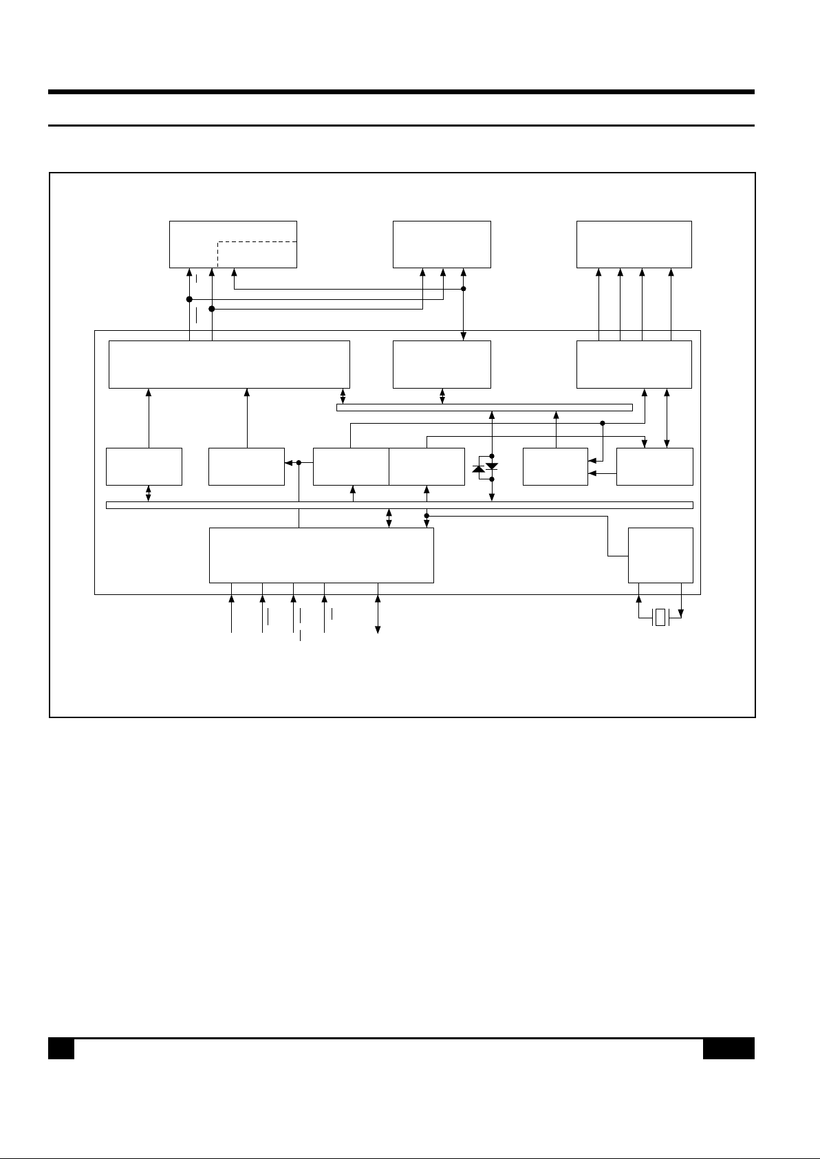
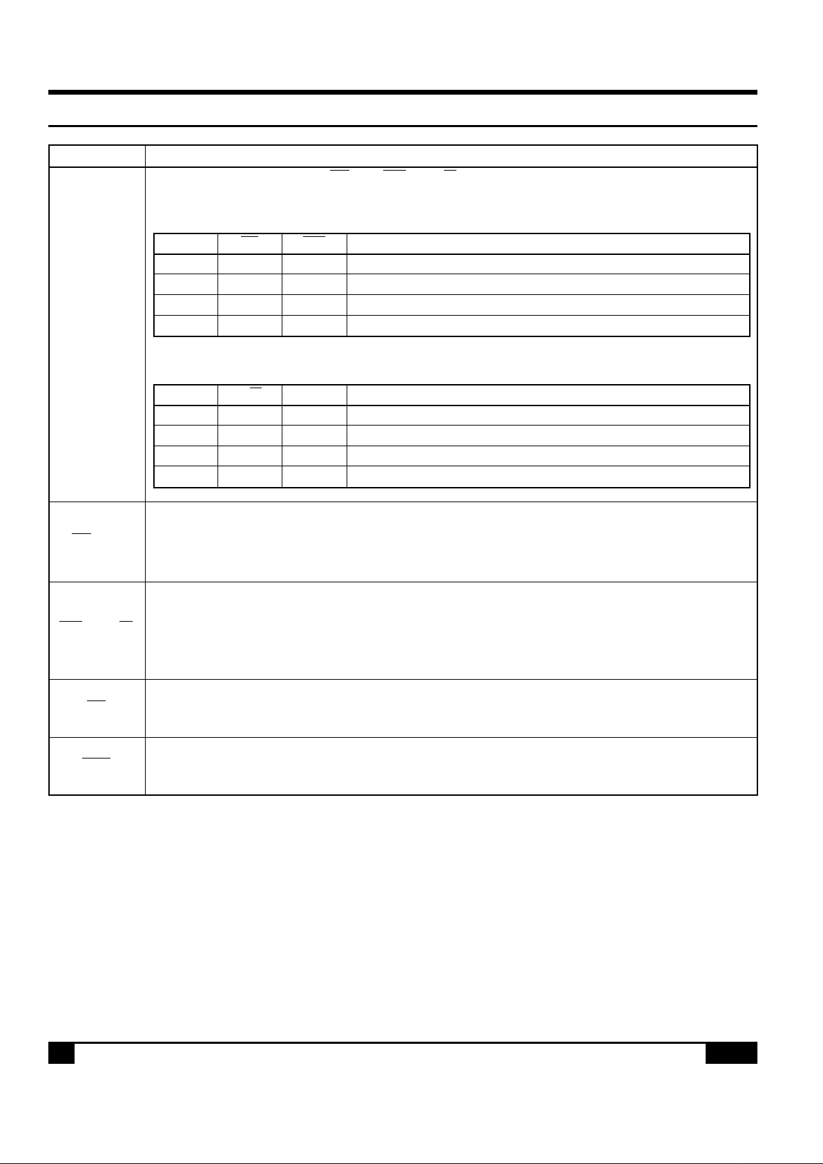
1.3 Block Diagram
Figure 1. SED1330F block diagram
Video RAM
Character
Generator RAM
Character
Generator ROM
LCD
LCD Controller
Input/Output
Register
Video RAM Interface
Display
Address
Controller
Cursor
Address
Controller
Refresh
Counter
Dot Counter
Layered
Controller
Character
Generator
ROM
OscillatorMicroprocessor Interface
YSCL,YD,YDIS
LP, WF
XSCL, XECL
XD0 to XD3
VD0 to VD7
VA0 to VA15
VCE
VR/W
SEL1
SEL0
RES
RD, WR
A0, CS
D0 to D7
OSC1 OSC2
Page 13
S-MOS Systems, Inc. • 2460 North First Street • San Jose, CA 95131 • Tel: (408) 922-0200 • Fax: (408) 922-0238
268-0.4 13
1.3 Block Diagram
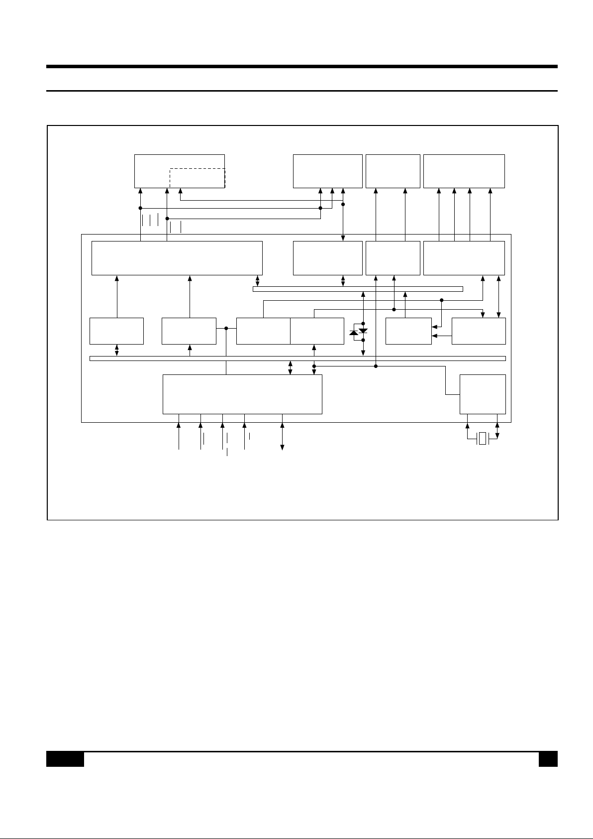
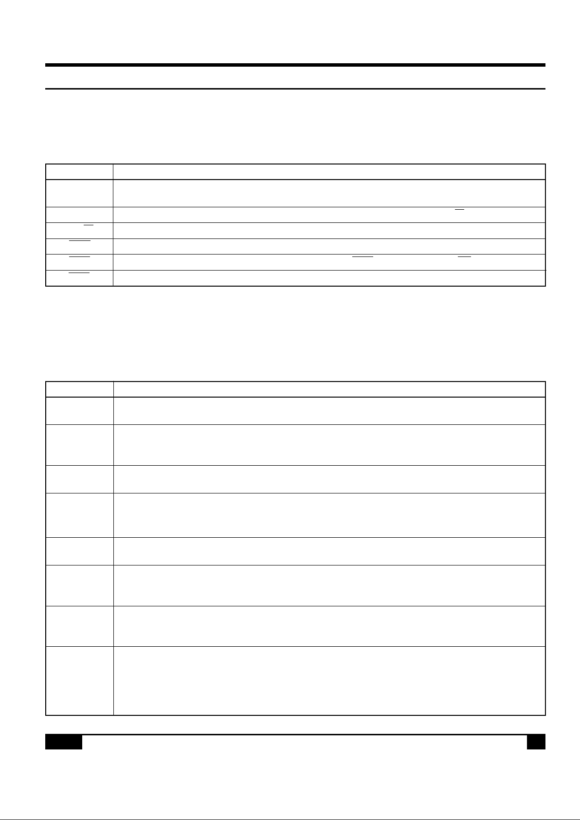
Figure 2. SED1335F/1336F block diagram
1.3 1.0 Overview
Video RAM
Character
Generator RAM
Character
Generator ROM
LCD ControllerVideo RAM Interface
Display
Address
Controller
Cursor
Address
Controller
Refresh
Counter
Dot Counter
Character
Generator
ROM
Layered
Controller
OscillatorMicroprocessor Interface
YSCL, YD, YDIS
LP, WF
XSCL, XECL
XD0 to XD3
VD0 to VD7
VA0 to VA15
VCE,
VRD,
VWR
VRD
VWR
SEL1
SEL0
RES
RD, WR
A0, CS
D0 to D7
XG
XD
TV
Controller*
Input/Output
Register
TV LCD
VSD
SNC
*SED1336F only
Page 14
S-MOS Systems, Inc. • 2460 North First Street • San Jose, CA 95131 • Tel: (408) 922-0200 • Fax: (408) 922-0238
14 268-0.4
1.0 Overview 1.4 – 1.4.2
1.4 Pinouts
Index
115
3145
46
60
SED1330FBB
16
30
XD3
D7
D6
D5
D4
D3
D2
D1
D0
V
DD
A0
CS
OSC2
OSC1
SEL 1
VD3
VD2
VD1
VD0
VA15
VA14
VA13
VA12
VA11
VA10
VA9
VA8
VA7
VA6
NC
VD4
VD5
VD6
VD7
YSCL
YD
YDIS
WF
LP
V
SS
XSCL
XECL
XD0
XD1
XD2
VA5
VA4
VA3
VA2
VA1
VA0
VR/W
VCE
NC
RES
NC
NC
RD
WR
SEL 2
Index
55
1
30
60
5
29
404550
201510
SED1330F
BA
VA8
VA9
VA10
VA11
VA12
VA13
NC
VA14
VA15
VD0
VD1
VD2
XD
CS
A0
V
DD
D0
D1
D2
D3
D4
D5
D6
D7
XD3
XD2
XD1
XD0
XECL
XSCL
V
SS
LP
WF
YDIS
YD
YSCL
VD7
VD6
VD5
VD4
VD3
XG
SEL1
SEL2WRRDNCNC
RESNCVCE
VWR
VA0
VA1
VA2
VA3
VA4
VA5
VA6
VA7
6
Figure 3. SED1330F and SED1335F pinouts
Index
115
3145
46
60
SED1335F0B
(SED1336F0A)
16
30
XD3
D7
D6
D5
D4
D3
D2
D1
D0
V
DD
A0
CS
XD
XG
SEL1
VD3
VD2
VD1
VD0
VA15
VA14
VA13
VA12
VA11
VA10
VA9
VA8
VA7
VA6
NC
VD4
VD5
VD6
VD7
YSCL(SNC)
YD
YDIS
WF
LP
V
SS
XSCL
XECL(VSD)
XD0
XD1
XD2
VA5
VA4
VA3
VA2
VA1
VA0
VWR
VCE
VRD
RES
NC
NC(CLO)
RD
WR
SEL 2(NT/PL)
Index
55
1
30
60
5
29
404550
201510
SED1335F
OA
VA8
VA9
VA10
VA11
VA12
VA13
NC
VA14
VA15
VD0
VD1
VD2
XD
CS
A0
V
DD
D0
D1
D2
D3
D4
D5
D6
D7
XD3
XD2
XD1
XD0
XECL
XSCL
V
SS
LP
WF
YDIS
YD
YSCL
VD7
VD6
VD5
VD4
VD3
XG
SEL1
SEL2
WR
RD
NC
NC
RES
VRD
VCE
VWR
VA0
VA1
VA2
VA3
VA4
VA5
VA6
VA7
6
Page 15
S-MOS Systems, Inc. • 2460 North First Street • San Jose, CA 95131 • Tel: (408) 922-0200 • Fax: (408) 922-0238
268-0.4 15
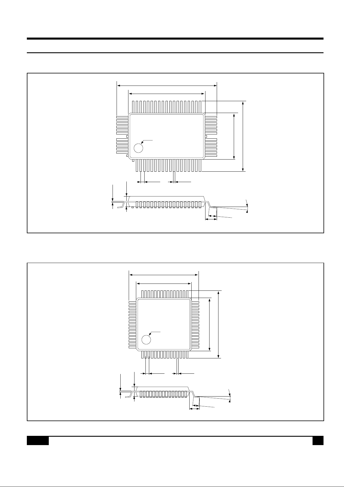
1.5 Package Dimensions
QFP5 Unit: mm
Figure 5. SED1330F
BB
, 1335F0B and SED1336F
0A
QFP6 Unit: mm
Index
115
31
16
45
46
60
30
0 ~ 12°
1.8
2.7
±
0.1
0.8 ±
0.3
0.15
±
0.05
0.35 ±
0.15
0.8 ±
0.15
17.6
±
0.4
14.0
±
0.2
17.6 ±
0.4
14.0 ±
0.2
0 ~ 12°
2.8
2.7
±
0.1
1.5 ±
0.3
0.15
±
0.05
Index
623
36
24
54
55
1
30
0.35 ±
0.1
19.6
±
0.4
14.0
±
0.1
25.6 ±
0.4
20.0 ±
0.1
60
5
29
35
1.0 ±
0.1
Figure 4. SED1330F
BA
and 1335F0A package dimensions
1.4 – 1.4.2 1.0 Overview
Page 16

S-MOS Systems, Inc. • 2460 North First Street • San Jose, CA 95131 • Tel: (408) 922-0200 • Fax: (408) 922-0238
16 268-0.4
THIS PAGE INTENTIONALLY BLANK
Page 17

S-MOS Systems, Inc. • 2460 North First Street • San Jose, CA 95131 • Tel: (408) 922-0200 • Fax: (408) 922-0238
268-0.4 17
2.0
Pin Description
Page 18
S-MOS Systems, Inc. • 2460 North First Street • San Jose, CA 95131 • Tel: (408) 922-0200 • Fax: (408) 922-0238
18 268-0.4
2.0 Pin Description
2.1 SED1330F
BA/BB
Pin Summary
2.0 Pin Description 2.0 – 2.1
Name
Number
Type Description
SED1330F
0A SED1330FBB
VA0 to VA15
27 to 28 50 to 59
Output VRAM address bus
30 to 43 1 to 6
VR/W 44 7 Output VRAM write signal
VCE 45 8 Output Memory control signal
RES 47 10 Input Reset
NC 29, 46, 48, 49 9, 11, 12, 60 — No connection
RD 50 13 Input
8080 family: Read signal
6800 family: Enable clock (E)
WR 51 14 Input
8080 family: Write signal
6800 family: R/W signal
SEL2 52 15 Input
8080 or 6800 family interface
select
SEL1 53 16 Input
8080 or 6800 family interface
select
OSC1 54 17 Input Oscillator connection
OSC2 55 18 Output Oscillator connection
CS 56 19 Input Chip select
A0 57 20 Input Data type select
V
DD 58 21 Supply 4.5 to 5.5V supply
D0 to D7
59 to 60
22 to 29 Input/output Data bus
1 to 6
XD0 to XD3 10 to 7 33 to 30 Output X-driver data
XECL 11 34 Output X-driver enable chain clock
XSCL 12 35 Output X-driver data shift clock
V
SS 13 36 Supply Ground
LP 14 37 Output Latch pulse
WF 15 38 Output Frame signal
YDIS 16 39 Output
Power-down signal when display is
blanked
YD 17 40 Output Scan start pulse
YSCL 18 41 Output Y-driver shift clock
VD0 to VD7 26 to 19 49 to 42 Input/output VRAM data bus
Page 19
S-MOS Systems, Inc. • 2460 North First Street • San Jose, CA 95131 • Tel: (408) 922-0200 • Fax: (408) 922-0238
268-0.4 19
2.0 – 2.2 2.0 Pin Description
2.0 Pin Description
2.2 SED1330F/1335F
0A/0B
Pin Summary
Name
Number
Type Description
SED1335F
0A SED1335F0B
VA0 to VA15
27 to 28 50 to 59
Output VRAM address bus
30 to 43 1 to 6
VWR 44 7 Output VRAM write signal
VCE 45 8 Output Memory control signal
VRD 46 9 Output VRAM read signal
RES 47 10 Input Reset
NC 29, 48, 49 11, 12, 60 — No connection
RD 50 13 Input
8080 family: Read signal
6800 family: Enable clock (E)
WR 51 14 Input
8080 family: Write signal
6800 family: R/W signal
SEL2 52 15 Input
8080 or 6800 family interface
select
SEL1 53 16 Input
8080 or 6800 family interface
select
XG 54 17 Input Oscillator connection
XD 55 18 Output Oscillator connection
CS 56 19 Input Chip select
A0 57 20 Input Data type select
V
DD 58 21 Supply 2.7 to 5.5V supply
D0 to D7
59 to 60
22 to 29 Input/output Data bus
1 to 6
XD0 to XD3 10 to 7 33 to 30 Output X-driver data
XECL 11 34 Output X-driver enable chain clock
XSCL 12 35 Output X-driver data shift clock
V
SS 13 36 Supply Ground
LP 14 37 Output Latch pulse
WF 15 38 Output Frame signal
YDIS 16 39 Output
Power-down signal when display is
blanked
YD 17 40 Output Scan start pulse
YSCL 18 41 Output Y-driver shift clock
VD0 to VD7 26 to 19 49 to 42 Input/output VRAM data bus
Page 20
S-MOS Systems, Inc. • 2460 North First Street • San Jose, CA 95131 • Tel: (408) 922-0200 • Fax: (408) 922-0238
20 268-0.4
2.0 Pin Description 2.3
2.3 SED1336F0A Pin Summary
Name Number Type Description
VA0 to VA15
1 to 6
Output VRAM address bus
50 to 59
VWR 7 Output VRAM write signal
VCE 8 Output Memory control signal
VRD 9 Output VRAM read signal
RES 10 Input Reset
NC 11, 60 — No connection
CLO 12 Output Clock output
RD 13 Input
8080 family: Read signal
6800 family: Enable clock (E)
WR 14 Input
8080 family: Write signal
6800 family: R/W signal
NT/PL 15 Input NTSC or PAL TV mode select
SEL1 16 Input 8080 or 6800 family interface select
OSC1 17 Input Oscillator connection
OSC2 18 Output Oscillator connection
CS 19 Input Chip select
A0 20 Input Data type select
V
DD 21 Supply 3.0 to 5.5V supply
D0 to D7 22 to 29 Input/output Data bus
XD0 to XD3 30 to 33 Output X-driver data
VSD 34 Output Video data
XSCL 35 Output Data shift clock
VSS 36 Supply Ground
LP 37 Output Latch pulse
WF 38 Output Frame signal
YDIS 39 Output
Power-down signal when display is
blanked
YD 40 Output Scan start pulse
SNC 41 Output TV sync signal
VD0 to VD7 42 to 49 Input/output VRAM data bus
Page 21
S-MOS Systems, Inc. • 2460 North First Street • San Jose, CA 95131 • Tel: (408) 922-0200 • Fax: (408) 922-0238
268-0.4 21
2.4 – 2.4.3 2.0 Pin Description
2.4 Pin Functions
2.4.1 Power Supply
Pin Name Function
V
DD
4.5 to 5.5V (SED1330F), 3.0 to 5.5V (SED1336F) or 2.7 to 5.5V (SED1330F/1335F) supply.
This may be the same supply as the controlling microprocessor.
V
SS Ground
Note: The peak supply current drawn by the SED1330F/1335F/1336F may be up to ten times the average supply current. The power
supply impedance must be kept as low as possible by ensuring that supply lines are sufficiently wide and by placing 0.47 µF
decoupling capacitors that have good high-frequency response near the device’s supply pins.
2.4.3 Microprocessor Interface
Pin Name Function
D0 to D7 Tristate input/output pins. Connect these pins to an 8- or 16-bit microprocessor bus.
Microprocessor interface select pin. The SED1336F supports both 8080 family processors
(such as the 8085 and Z80®) and 6800 family processors (such as the 6802 and 6809).
SEL1* SEL2 Interface A0 RD WR CS
0 0 8080 family A0 RD WR CS
1 0 6800 family A0 E R/W CS
* SED1330F and SED1335F only
Note: SEL1 should be tied directly to VDD or VSS to prevent noise. If noise does appear on SEL1, decouple it to ground using a
capacitor placed as close to the pin as possible.
SEL1, SEL2
2.4.2 Oscillator
Pin Name Function
(OSC) XG
Crystal connection for internal oscillator (see Section 8.3). This pin can be driven by an external
clock source that satisfies the timing specifications of the EXT φ0 signal (see Section 4.3.6).
(OSC2) XD
Crystal connection for internal oscillator. Leave this pin open when using an external clock
source.
CLO
Clock output (SED1336F only). Same phase as XG. Clock is output when system command
P1 is executed. Output stops during system reset.
Page 22
S-MOS Systems, Inc. • 2460 North First Street • San Jose, CA 95131 • Tel: (408) 922-0200 • Fax: (408) 922-0238
22 268-0.4
2.0 Pin Description 2.4.3
Pin Name Function
A0, in conjunction with the RD and WR or R/W and E signals, controls the type of access to
the SED1336F, as shown below.
8080 family interface
A0 RD WR Function
0 0 1 Status flag read
1 0 1 Display data and cursor address read
0 1 0 Display data and parameter write
1 1 0 Command write
6800 family interface
A0 R/W E Function
0 1 1 Status flag read
1 1 1 Display data and cursor address read
0 0 1 Display data and parameter write
1 0 1 Command write
When the 8080 family interface is selected, this signal acts as the active-LOW read strobe. The
SED1330F/1335F/1336F’s output buffers are enabled when this signal is active.
When the 6800 family interface is selected, this signal acts as the active-HIGH enable clock.
Data is read from or written to the SED1330F/1335F/1336F when this clock goes HIGH.
When the 8080 family interface is selected, this signal acts as the active-LOW write strobe. The
bus data is latched on the rising edge of this signal.
When the 6800 family interface is selected, this signal acts as the read/write control signal. Data
is read from the SED1330F/1335F/1336F if this signal is HIGH, and written to the SED1330F/
1335F/1336F if it is LOW.
Chip select. This active-LOW input enables the SED1330F/1335F/1336F. It is usually
connected to the output of an address decoder device that maps the SED1330F/1335F/1336F
into the memory space of the controlling microprocessor.
This active-LOW input performs a hardware reset on the SED1330F/1335F/1336F. It is a
Schmitt-trigger input for enhanced noise immunity; however, care should be taken to ensure
that it is not triggered if the supply voltage is lowered.
WR or R/W
CS
RES
RD or E
A0
Page 23
S-MOS Systems, Inc. • 2460 North First Street • San Jose, CA 95131 • Tel: (408) 922-0200 • Fax: (408) 922-0238
268-0.4 23
2.4.4 – 2.4.5 2.0 Pin Description
2.4.4 Display Memory Control
The SED1330F/1335F/1336F can directly access static
RAM and PROM. The designer may use a mixture of
these two types of memory to achieve an optimum
trade-off between low cost and low power consumption.
Pin Name Function
VA0 to VA15
16-bit display memory address. When accessing character generator RAM or ROM, VA0 to
VA3, reflect the lower 4 bits of the row counter.
VD0 to VD7 8-bit tristate display memory data bus. These pins are enabled when VR/W is LOW.
VR/W Active-LOW display memory write control output (SED1330).
VRD Active-LOW display memory read control output (SED1335/6).
VCE Active-LOW static memory standby control signal. VCE can be used with CS.
VWR Active-LOW display memory write control output (SED1335/6).
2.4.5 LCD Drive Signals
In order to provide effective low-power drive for LCD
matrixes, the SED1330F/1335F/1336F can directly
control both the X- and Y-drivers using an enable
chain.
Pin Name Function
XD0 to XD3
4-bit X-driver (column drive) data outputs. Connect these outputs to the inputs of the X-driver
chips.
The falling edge of XSCL latches the data on XD0 to XD3 into the input shift registers of the
X-drivers. To conserve power, this clock halts between LP and the start of the following display
line (see Section 4.3.7).
XECL
The falling edge of XECL (SED1330F/1335F only) triggers the enable chain cascade for the
X-drivers (SED1600/SED1180). Every 16th clock pulse is output to the next X-driver.
LP latches the signal in the X-driver shift registers into the output data latches. LP is a fallingedge triggered signal, and pulses once every display line.
Connect LP to the Y-driver shift clock on modules that use the SED1600 and SED1610 drivers.
WF
LCD panel AC drive output. The WF period is selected to be one of two values with SYSTEM
SET command.
The falling edge of YSCL (SED1330F/1335F only) latches the data on YD into the input shift
registers of the Y-drivers. YSCL is not used with the SED1600, SED1610 or other driver ICs
which use LP as the Y-driver shift clock.
YD is the data pulse output for the Y drivers. It is active during the last line of each frame, and
is shifted through the Y drivers one by one (by YSCL), to scan the display’s common
connections.
Power-down output signal. YDIS is HIGH while the display drive outputs are active.
YDIS goes LOW one or two frames after the sleep command is written to the SED1330F/
1335F/1336F. All Y-driver outputs are forced to an intermediate level (de-selecting the display
segments) to blank the display. In order to implement power-down operation in the LCD unit,
the LCD power drive supplies must also be disabled when the display is disabled by YDIS.
XSCL
LP
YSCL
YD
YDIS
Page 24

S-MOS Systems, Inc. • 2460 North First Street • San Jose, CA 95131 • Tel: (408) 922-0200 • Fax: (408) 922-0238
24 268-0.4
1.0 Overview 1.3
THIS PAGE INTENTIONALLY BLANK
Page 25

S-MOS Systems, Inc. • 2460 North First Street • San Jose, CA 95131 • Tel: (408) 922-0200 • Fax: (408) 922-0238
268-0.4 25
1.3 – 1.4 1.0 Overview
3.0
Command Description
Page 26

S-MOS Systems, Inc. • 2460 North First Street • San Jose, CA 95131 • Tel: (408) 922-0200 • Fax: (408) 922-0238
26 268-0.4
THIS PAGE INTENTIONALLY BLANK
Page 27

S-MOS Systems, Inc. • 2460 North First Street • San Jose, CA 95131 • Tel: (408) 922-0200 • Fax: (408) 922-0238
268-0.4 27
3.0 – 3.1 3.0 Command Description
3.0 Command Description
3.1 The Command Set
Table 1. The Command Set
Command
Code Read
Class Command Hex Command Description
Parameters
RD WR A0 D7 D6 D5 D4 D3 D2 D1 D0
No. of SecBytes tion
SYSTEM SET 1010100000040
Initialize device and dis-
8 3.2.1
play
SLEEP IN 1010101001153Enter standby mode 0 3.2.2
DISP ON/OFF 1010101100D
58, Enable and disable dis-
1 3.3.1
59 play and display flashing
SCROLL 1010100010044
Set display start address
10 3.3.2
and display regions
CSRFORM 101010111015DSet cursor type 2 3.3.3
CGRAM ADR 101010111005C
Set start address of char-
2 3.3.6
acter generator RAM
CD CD
4C
Set direction of cursor
CSRDIR 101010011
10
to
movement
0 3.3.4
4F
HDOT SCR 101010110105A
Set horizontal scroll pos-
1 3.3.7
ition
OVLAY 101010110115B
Set display overlay for-
1 3.3.5
mat
CSRW 1010100011046Set cursor address 2 3.4.1
CSRR 1010100011147Read cursor address 2 3.4.2
MWRITE 1010100001042Write to display memory — 3.5.1
MREAD 1010100001143
Read from display mem-
— 3.5.2
ory
Notes:
1. In general, the internal registers of the SED1330F/1335F/1336F are modified as each command parameter is input. However,
the microprocessor does not have to set all the parameters of a command and may send a new command before all parameters
have been input. The internal registers for the parameters that have been input will have been changed but the remaining
parameter registers are unchanged.
2-byte parameters (where two bytes are treated as one data item) are handled as follows:
a. CSRW, CSRR: Each byte is processed individually. The microprocessor may read or write just the low byte of the cursor
address.
b. SYSTEM SET, SCROLL, CGRAM ADR: Both parameter bytes are processed together. If the command is changed after
half of the parameter has been input, the single byte is ignored.
2. APL and APH are 2-byte parameters, but are treated as two 1-byte parameters.
System
control
Display
control
Drawing
control
Memory
control
Page 28

S-MOS Systems, Inc. • 2460 North First Street • San Jose, CA 95131 • Tel: (408) 922-0200 • Fax: (408) 922-0238
28 268-0.4
3.0 Command Description 3.2 – 3.2.1
3.2 System Control Commands
3.2.1 SYSTEM SET
Initializes the device, sets the window sizes, and
selects the LCD interface format. Since the command
sets the basic operating parameters of the SED1330F/
1335F/1336F, an incorrect SYSTEM SET command
may cause other commands to operate incorrectly.
C 01000000 1 0 1
D7 D6 D5 D4 D3 D2 D1 D0 A0 WR RD
P1 DR T/L IV 1 W/S M2 M1 M0 0 0 1
P2 WF0000 FX 0 0 1
P3 0000 FY 0 0 1
P4 C/R 0 0 1
P5 TC/R 0 0 1
P6 L/F 0 0 1
P7 APL 0 0 1
P8 APH 0 0 1
LSBMSB
Figure 7. SYSTEM SET instruction
Page 29

S-MOS Systems, Inc. • 2460 North First Street • San Jose, CA 95131 • Tel: (408) 922-0200 • Fax: (408) 922-0238
268-0.4 29
3.2.1.1 – 3.2.1.5 3.0 Command Description
3.2.1.1 C
This control byte performs the following:
1. Resets the internal timing generator
2. Disables the display
3. Cancels sleep mode
Parameters following P1 are not needed if only canceling sleep mode.
3.2.1.2 M0
Selects the internal or external character generator
ROM. The internal character generator ROM contains 160, 5 × 7 pixel characters. These characters are
fixed at fabrication by the metalization mask. The
external character generator ROM can contain up to
256 user-defined characters.
M0 = 0: Internal CG ROM
M0 = 1: External CG ROM
Note that if the CG ROM address space overlaps the
display memory address space, that portion of the
display memory cannot be written to.
3.2.1.3 M1
Selects the CG RAM area for user-definable characters. The CG RAM codes are selected from the 64
codes shown in Figure 59.
M1 = 0: CG RAM1; 32 char
The CG RAM1 and CG RAM2 address spaces are not
contiguous, the CG RAM1 address space is treated
as character generator RAM, and the CG RAM2
address space is treated as character generator ROM.
M1 = 1: 64 char CG RAM + CG RAM2
The CG RAM1 and CG RAM2 address spaces are
contiguous and are both treated as character generator RAM.
3.2.1.4 M2
Selects the height of the character defined in external
CG ROM and CG RAM. Characters more than 16 pixels high can be displayed by creating a bitmap for
each portion of each character and using the
SED1330F/1335F/1336F’s graphics mode to reposition them.
M2 = 0: 8-pixel character height (2716 or
equivalent ROM)
M2 = 1: 16-pixel character height (2732
or equivalent ROM)
3.2.1.5 W/S
Selects the LCD drive method.
W/S = 0: Single-panel drive
W/S = 1: Dual-panel drive
Page 30
S-MOS Systems, Inc. • 2460 North First Street • San Jose, CA 95131 • Tel: (408) 922-0200 • Fax: (408) 922-0238
30 268-0.4
3.0 Command Description 3.2.1.5
Figure 8. Single-panel display
Figure 9. Dual-panel display
EI
X driver X driver
LCD
Y driver
YD
EI
X driver X driver
YD
X driver X driver
Upper Panel
Lower Panel
Y driver
Page 31

S-MOS Systems, Inc. • 2460 North First Street • San Jose, CA 95131 • Tel: (408) 922-0200 • Fax: (408) 922-0238
268-0.4 31
3.2.1.5 3.0 Command Description
EI
YD
Y driver
X driver X driver X driver X driver
Right PanelLeft Panel
Note: There are no Seiko-Epson LCD units in the configuration shown in Figure 10.
Figure 10. Left-and-right two-panel display
Table 3. LCD parameters
Parameter
W/S = 0 W/S = 1
IV = 1 IV = 0 IV = 1 IV = 0
C/R C/R C/R C/R C/R
TC/R TC/R TC/R (see note 1) TC/R TC/R
L/F L/F L/F L/F L/F
SL1 00H to L/F
00H to L/F + 1
(L/F) / 2 (L/F) / 2
(see note 2)
SL2 00H to L/F
00H to L/F + 1
(L/F) / 2 (L/F) / 2
(see note 2)
SAD1 First screen block First screen block First screen block First screen block
SAD2 Second screen block Second screen block Second screen block Second screen block
SAD3 Third screen block Third screen block Third screen block Third screen block
SAD4 Invalid Invalid Fourth screen block Fourth screen block
Cursor move-
Continuous movement over whole screen
Above-and-below configuration:
ment range continuousmovement over whole screen
Notes:
1. See table 31 (page 105) for further details on setting the C/R and TC/R parameters when using the HDOT SCR command.
2. The value of SL when IV = 0 is equal to the value of SL when IV = 1, plus one.
Page 32

S-MOS Systems, Inc. • 2460 North First Street • San Jose, CA 95131 • Tel: (408) 922-0200 • Fax: (408) 922-0238
32 268-0.4
3.0 Command Description 3.2.1.6 – 3.2.1.9
3.2.1.6 IV
Screen origin compensation for inverse display. IV is
usually set to 1.
The best way of displaying inverted characters is to
Exclusive-OR the text layer with the graphics background layer. However, inverted characters at the top
or left of the screen are difficult to read as the character origin is at the top-left of its bitmap and there are no
background pixels either above or to the left of these
characters.
The IV flag causes the SED1330F/1335F/1336F to
offset the text screen against the graphics back layer
by one vertical pixel. Use the horizontal pixel scroll
function (HDOT SCR) to shift the text screen 1 to 7
pixels to the right. All characters will then have the
necessary surrounding background pixels that ensure easy reading of the inverted characters.
See Section 5.5 for information on scrolling.
IV = 0: Screen top-line correction
IV = 1: No screen top-line correction (no
offset)
3.2.1.7 T/L
Selects TV or LCD mode. When TV mode is selected,
the TV sync generator circuit is ON.
T/L = 0: LCD mode
T/L = 1: TV mode
3.2.1.9 FX
Sets the width, in pixels, of the character field. The
character width in pixels is equal to FX + 1, where FX
can range from 00 to 07H inclusive. If data bit 3 is set
(FX is in the range 08 to 0FH) and an 8-pixel font is
used, a space is inserted between characters. Note
that the maximum character width in TV mode is eight
pixels.
Table 4. Horizontal character size selection
FX
[FX] character width
HEX D3 D2 D1 D0
(pixels)
00 0000 1
01 0001 2
↓ ↓↓↓↓ ↓
07 0111 8
Since the SED1330F/1335F/1336F handles display
data in 8-bit units, characters larger than 8 pixels wide
must be formed from 8-pixel segments. As Figure 12
shows, the remainder of the second eight bits are not
displayed. This also applies to the second screen layer.
In graphics mode, the normal character field is also
eight pixels. If a wider character field is used, any
remainder in the second eight bits is not displayed.
3.2.1.8 DR
Selects output of an additional shift-clock cycle for
every 64 pixels. The extra cycles are required for
correct operation of the enable chain when using a
two-panel display.
DR = 0: Normal operation
DR = 1: Additional shift-clock cycles
IV
1 dot
Dots 1 to 7
Display start point
Back layer
HDOT SCR
Character
Figure 11. IV and HDOT SCR adjustment
Page 33

S-MOS Systems, Inc. • 2460 North First Street • San Jose, CA 95131 • Tel: (408) 922-0200 • Fax: (408) 922-0238
268-0.4 33
3.2.1.10 – 3.2.1.11 3.0 Command Description
8 bits
FY
FX
8 bits
FY
FX
Non-display areaAddress BAddress A
8 bits
8 bits
Figure 12. FX and FY display addresses
3.2.1.10 WF
Selects the AC frame drive waveform period. WF is
usually set to 1.
WF = 0: 16-line AC drive
WF = 1: two-frame AC drive
In two-frame AC drive, the WF period is twice the
frame period.
In 16-line AC drive, WF inverts every 16 lines.
Although 16-line AC drive gives a more readable
display, horizontal lines may appear when using high
LCD drive voltages or at high viewing angles.
3.2.1.11 FY
Sets the height, in pixels, of the character. The height
in pixels is equal to FY + 1.
FY can range from 00 to 0FH inclusive.
Set FY to zero (vertical size equals one) when in
graphics mode.
Table 5. Vertical character size selection
FY
[FY] character
HEX D3 D2 D1 D0
height (pixels)
00 0000 1
01 0001 2
↓ ↓↓↓↓ ↓
07 0111 8
↓ ↓↓↓↓ ↓
0E1110 15
0F 1111 16
Page 34

S-MOS Systems, Inc. • 2460 North First Street • San Jose, CA 95131 • Tel: (408) 922-0200 • Fax: (408) 922-0238
34 268-0.4
3.0 Command Description 3.2.1.12 – 3.2.1.13
3.2.1.12 C/R
Sets the address range covered by one display line,
that is, the number of characters less one, multiplied
by the number of horizontal bytes per character.
C/R can range from 0 to 239.
For example, if the character width is 10 pixels, then
the address range is equal to twice the number of
characters, less 2. See Section 9.1.1 for the calculation of C/R.
[C/R] cannot be set to a value greater than the
address range. It can, however, be set smaller than
the address range, in which case the excess display
area is blank. The number of excess pixels must not
exceed 64.
Table 6. Display line address range
C/R
[C/R] bytes per display line
HEX D7 D6 D5 D4 D3 D2 D1 D0
00 00000000 1
01 00000001 2
↓ ↓↓↓↓↓↓↓↓ ↓
4F 01001111 80
↓ ↓↓↓↓↓↓↓↓ ↓
EE11101110 239
EF11101111 240
3.2.1.13 TC/R
Sets the length, including horizontal blanking, of one
line. The line length is equal to TC/R + 1, where TC/
R can range from 0 to 255.
TC/R must be greater than or equal to C/R + 4.
Provided this condition is satisfied, [TC/R] can be set
according to the equation given in section 9.1.1 in
order to hold the frame period constant and minimize
jitter for any given main oscillator frequency, f
OSC
.
Table 7. Line length selection
TC/R
[TC/R] line length (bytes)
HEX D7 D6 D5 D4 D3 D2 D1 D0
00 00000000 1
01 00000001 2
↓ ↓↓↓↓↓↓↓↓ ↓
52 01010010 83
↓ ↓↓↓↓↓↓↓↓ ↓
FE11111110 255
FF 11111111 256
Page 35

S-MOS Systems, Inc. • 2460 North First Street • San Jose, CA 95131 • Tel: (408) 922-0200 • Fax: (408) 922-0238
268-0.4 35
3.2.1.14 – 3.2.1.15 3.0 Command Description
3.2.1.14 L/F
Sets the height, in lines, of a frame. The height in lines
is equal to L/F + 1, where L/F can range from 0 to 255.
If W/S is set to 1, selecting two-screen display, the
number of lines must be even and L/F must, therefore,
be an odd number.
Table 8. Frame height selection
L/F
[L/F] lines per frame
HEX D7 D6 D5 D4 D3 D2 D1 D0
00 00000000 1
01 00000001 2
↓ ↓↓↓↓↓↓↓↓ ↓
7F 01111111 128
↓ ↓↓↓↓↓↓↓↓ ↓
FE11111110 255
FF 11111111 256
Table 9. Frame heights and compatible LCD units
Number of lines [LF] Panel Duty Cycle
64 1/64
128 1/64
Table 10. Horizontal address range
Hex code
[AP] addresses
APH APL
per line
0000 0
0001 1
↓↓↓↓ ↓
0050 80
↓↓↓↓ ↓
FFFE 216 – 2
FFFF 216 – 1
3.2.1.15 AP
Defines the horizontal address range of the virtual
screen. APL is the least significant byte of the address.
Figure 13. AP parameters
APL AP7 AP6 AP5 AP4 AP3 AP2 AP1 AP0
APH AP15 AP14 AP13 AP12 AP11 AP10 AP9 AP8
Page 36

S-MOS Systems, Inc. • 2460 North First Street • San Jose, CA 95131 • Tel: (408) 922-0200 • Fax: (408) 922-0238
36 268-0.4
3.0 Command Description 3.2.1.15 – 3.3.1
Figure 14. AP and C/R relationship
3.2.2 SLEEP IN
Places the system in standby mode. This command
has no parameter bytes. At least one blank frame after
receiving this command, the SED1330F/1335F/1336F
halts all internal operations, including the oscillator,
and enters the sleep mode. Blank data is sent to the
X-drivers, and the Y-drivers have their bias supplies
turned off by the YDIS signal. Using the YDIS signal
to disable the Y-drivers guards against any spurious
displays.
The internal registers of the SED1330F/1335/1336F
maintain their values during the sleep mode. The
display memory control pins maintain their logic levels
to ensure that the display memory is not corrupted.
The SED1330F/1335F/1336F can be removed from
the sleep state by sending the SYSTEM SET command with only the P1 parameter. The DISP ON
command should be sent next to enable the display.
Figure 15. SLEEP IN instruction
1. The YDIS signal goes LOW between one
and two frames after the SLEEP IN command is received. Since YDIS forces all
display driver outputs to go to the deselected output voltage, YDIS can be used as
a power-down signal for the LCD unit. This
can be done by having YDIS turn off the
relatively high-power LCD drive supplies at
the same time as it blanks the display.
2. Since all internal clocks in the SED1330F/
1335F/1336F are halted while in the sleep
state, a DC voltage will be applied to the LCD
panel if the LCD drive supplies remain on.
If reliability is a prime consideration, turn off
the LCD drive supplies before issuing the
SLEEP IN command.
3. Note that, although the bus lines become
high impedance in the sleep state, pull-up
or pull-down resistors on the bus line will
force these lines to a known state.
3.3 Display Control Commands
3.3.1 DISP ON/OFF
Turns the whole display on or off. The single-byte
parameter enables and disables the cursor and layered screens, and sets the cursor and screen flash
rates. The cursor can be set to flash over one character or over a whole line.
MSB LSB
C01010011
Figure 16. DISP ON/OFF parameters
MSB LSB
C01011000
P1 FP5 FP4 FP3 FP2 FP1 FP0 FC1 FC0
Display area
C/R
Display memory limit
AP
Page 37

S-MOS Systems, Inc. • 2460 North First Street • San Jose, CA 95131 • Tel: (408) 922-0200 • Fax: (408) 922-0238
268-0.4 37
3.3.1.1 – 3.3.2.1 3.0 Command Description
3.3.1.1 D
Turns the display ON or OFF. The D bit takes precedence over the FP bits in the parameter.
D = 0: Display OFF
D = 1: Display ON
3.3.1.2 FC
Enables/disables the cursor and sets the flash rate.
The cursor flashes with a 70% duty cycle (ON/OFF).
Table 11. Cursor flash rate selection
FC1 FC0 Cursor display
0 0 OFF (blank)
0 1 No flashing
10
Flash at f
FR/32 Hz
(approx. 2 Hz)
11
Flash at f
FR/64 Hz
(approx. 1 Hz)
Note: As the MWRITE command always enables the cursor,
the cursor position can be checked even when performing consecutive writes to display memory while the
cursor is flashing.
3.3.1.3 FP
Each pair of bits in FP sets the attributes of one screen
block, as follows.
Table 12. Screen block attribute selection
FP1 FP0 First screen block (SAD1)
FP3 FP2
Second screen block (SAD2,
SAD4). See note.
FP5 FP4 Third screen block (SAD3)
0 0 OFF (blank)
0 1 No flashing
10
Flash at f
FR/32 Hz
(approx. 2 Hz)
11
Flash at f
FR/4 Hz
(approx. 16 Hz)
Note: If SAD4 is enabled by setting W/S to 1, FP3 and FP2
control both SAD2 and SAD4. The attributes of SAD2
and SAD4 cannot be set independently.
3.3.2 SCROLL
3.3.2.1 C
Sets the scroll start address and the number of lines
per scroll block. Parameters P1 to P10 can be omitted
if not required. The parameters must be entered
sequentially as shown in Figure 17.
ON
ON
MSB LSB
C01000100
P1 A7 A6 A5 A4 A3 A2 A1 A0 (SAD 1L)
P2 A15 A14 A13 A12 A11 A10 A9 A8 (SAD 1H)
P3 L7 L6 L5 L4 L3 L2 L1 L0 (SL 1)
P4 A7 A6 A5 A4 A3 A2 A1 A0 (SAD 2 L)
P5 A15 A14 A13 A12 A11 A10 A9 A8 (SAD 2H)
P6 L7 L6 L5 L4 L3 L2 L1 L0 (SL 2)
P7 A7 A6 A5 A4 A3 A2 A1 A0 (SAD 3L)
P8 A15 A14 A13 A12 A11 A10 A9 A8 (SAD 3H)
P9 A7 A6 A5 A4 A3 A2 A1 A0 (SAD 4L)
P10 A15 A14 A13 A12 A11 A10 A9 A8 (SAD 4H)
Note: Set parameters P9 and P10 only if both two-screen
drive (W/S = 1) and two-layer configuration are selected. SAD4 is the fourth screen block display start
address.
Figure 17. SCROLL instruction parameters
Page 38

S-MOS Systems, Inc. • 2460 North First Street • San Jose, CA 95131 • Tel: (408) 922-0200 • Fax: (408) 922-0238
38 268-0.4
3.0 Command Description 3.3.2.1 – 3.3.2.2
Table 13. Screen block start address selection
SL1, SL2
[SL] screen lines
HEX L7 L6 L5 L4 L3 L2 L1 L0
00 00000000 1
01 00000001 2
↓ ↓↓↓↓↓↓↓↓ ↓
7F 01111111 128
↓ ↓↓↓↓↓↓↓↓ ↓
FE11111110 255
FF 11111111 256
3.3.2.2 SL1, SL2
SL1 and SL2 set the number of lines per scrolling
screen. The number of lines is SL1 or SL2 plus one.
The relationship between SAD, SL and the display
mode is described below.
Table 14. Text display mode
W/S Screen First Layer Second Layer
First screen block SAD1 SAD2
Second screen block SL1 SL2
SAD3 (see note 1)
Third screen block (partitioned screen) Set both SL1 and SL2 to L/F + 1
if not using a partitioned screen.
Screen configuration example:
0
(continued)
Character display page 1
Character display page 3
SAD2
SAD1
SAD3
SL1
SL2
Graphics display page 2
Layer 2
La
y
er 1
Page 39

S-MOS Systems, Inc. • 2460 North First Street • San Jose, CA 95131 • Tel: (408) 922-0200 • Fax: (408) 922-0238
268-0.4 39
3.3.2.2 3.0 Command Description
Table 14. Text display mode (continued)
W/S Screen First Layer Second Layer
Upper screen
SAD1 SAD2
SL1 SL2
Lower screen
SAD3 SAD4
(see note 2) (see note 2)
Set both SL1 and SL2 to ((L/F) / 2 + 1)
Screen configuration example:
1
Notes:
1. SAD3 has the same value as either SAD1 or SAD2, whichever has the least number of lines (set by SL1 and SL2).
2. Since the parameters corresponding to SL3 and SL4 are fixed by L/F, they do not have to be set in this mode.
Character display page 1
Character display page 3
SAD2
SAD1
SAD3
SL1
Graphics display page 2
La
y
er 2Layer 1
Graphics display page 4
(SAD4)
Page 40

S-MOS Systems, Inc. • 2460 North First Street • San Jose, CA 95131 • Tel: (408) 922-0200 • Fax: (408) 922-0238
40 268-0.4
3.0 Command Description 3.3.2.2
Table 15. Graphics display mode
W/S Screen First Layer Second Layer Third Layer
Two-layer composition
SAD1 SAD2
SL1 SL2
SAD3 (see note 3)
Upper screen
Set both SL1 and SL2 to
L/F + 1 if not using a
partitioned screen
Screen configuration example:
0
0
Three-layer configuration
SAD1 SAD2 SAD3
SL1 = L/F + 1 SL2 = L/F + 1 —
Screen configuration example:
Character display page 1
Character display page 3
SAD2
SAD1
SAD3
SL1
SL2
Graphics display page 2
Layer 1 Layer 2
Graphics display page 1
SAD2
SAD1
SAD3
SL1
SL2
Graphics display page 2
Layer 1
Graphics display page 3
Layer 2
Layer 3
Page 41

S-MOS Systems, Inc. • 2460 North First Street • San Jose, CA 95131 • Tel: (408) 922-0200 • Fax: (408) 922-0238
268-0.4 41
3.3.2.2 3.0 Command Description
Notes:
1. SAD3 has the same value as either SAD1 or SAD2, whichever has the least number of lines (set by SL1 and SL2).
2. Since the parameters corresponding to SL3 and SL4 are fixed by L/F, they do not have to be set.
3. If, and only if, W/S = 1, the differences between SL1 and (L/F + 1) / 2, and between SL2 and (L/F + 1) / 2, are blanked.
Table 15. Graphics display mode (continued)
W/S Screen First Layer Second Layer Third Layer
Upper screen
SAD1 SAD2
—
SL1 SL2
Lower screen
SAD3 SAD4
—
(see note 2) (see note 2)
Set both SL1 and SL2 to ((L/F) / 2 + 1)
Screen configuration example (see note 3):
1
Figure 18. Two-panel display height
Graphics display page 1
Graphics display page 3
SAD2
SAD1
SAD3
SL1
Graphics display page 2
Layer 2Layer 1
Graphics display page 4
Upper Panel
Lower Panel
SL1
L/2
L
Graphics
Page 42

S-MOS Systems, Inc. • 2460 North First Street • San Jose, CA 95131 • Tel: (408) 922-0200 • Fax: (408) 922-0238
42 268-0.4
MSB LSB
C01011101
P10000
X3 X2
CRX
X1 X0
P2 CM 0 0 0
Y3 Y2
CRY
Y1 Y0
3.0 Command Description 3.3.3 – 3.3.3.2
3.3.3 CSRFORM
Sets the cursor size and display mode. Although the
cursor is normally only used in text displays, it may
also be used in graphics displays when displaying
special characters.
3.3.3.2 CRY
Sets the location of an underscored cursor in lines,
from the character origin. When using a block cursor,
CRY sets the vertical size of the cursor from the
character origin. CRY is equal to the number of lines
less one.
Table 17. Cursor height selection
CRY
[CRY] cursor
HEX Y3 Y2 Y1 Y0
height (lines)
0 0000 illegal
1 0001 2
↓ ↓↓↓↓ ↓
8 1000 9
↓ ↓↓↓↓ ↓
E 1110 15
F 1111 16
Figure 20. Cursor size and position
Figure 19. CSRFORM parameter bytes
3.3.3.1 CRX
Sets the horizontal size of the cursor from the character origin. CRX is equal to the cursor size less one.
CRX must be less than or equal to FX.
Table 16. Horizontal cursor size selection
CRX
[CRX] cursor width
HEX X3 X2 X1 X0
(pixels)
0 0000 1
1 0001 2
↓ ↓↓↓↓ ↓
8 1000 9
↓ ↓↓↓↓ ↓
E 1110 15
F 1111 16
0123456•• •
0
1
2
3
4
5
6
7
8
9
Character start point
CRX = 5 dots
CRY = 9 dots
CM = 0
Page 43

S-MOS Systems, Inc. • 2460 North First Street • San Jose, CA 95131 • Tel: (408) 922-0200 • Fax: (408) 922-0238
268-0.4 43
3.3.3.3 – 3.3.5.1 3.0 Command Description
3.3.3.3 CM
Sets the cursor display mode. Always set CM to 1
when in graphics mode.
CM = 0: Underline cursor
CM = 1: Block cursor
3.3.4 CSRDIR
Sets the direction of automatic cursor increment. The
cursor can move left or right one character, or up or
down by the number of bytes specified by the address
pitch, AP.
When reading from and writing to display memory,
this automatic cursor increment controls the display
memory address increment on each read or write.
Table 18. Cursor shift direction
C CD1 CD0 Shift direction
4CH 0 0 Right
4DH 0 1 Left
4EH 1 0 Up
4FH 1 1 Down
Note: Since the cursor moves in address units even if FX ≥ 9,
the cursor address increment must be preset for movement in character units. See Section 5.3.
3.3.5 OVLAY
Selects layered screen composition and screen text/
graphics mode.
MSB LSB
C010011CD1CD2
Figure 21. CSRDIR parameters
Figure 22. Cursor direction
MSB LSB
C01011011
P1 0 0 0 OV DM2 DM1 MX1 MX0
Figure 23. OVLAY parameter
3.3.5.1 MX0, MX1
MX0 and MX1 set the layered screen composition
method, which can be either OR, AND, Exclusive-OR
or Priority-OR. Since the screen composition is organized in layers and not by screen blocks, when using
a layer divided into two screen blocks, different composition methods cannot be specified for the individual screen blocks.
The Priority-OR mode is the same as the OR mode
unless flashing of individual screens is used.
10
11
0001
–1 +1
+AP
–AP
Page 44

S-MOS Systems, Inc. • 2460 North First Street • San Jose, CA 95131 • Tel: (408) 922-0200 • Fax: (408) 922-0238
44 268-0.4
3.0 Command Description 3.3.5.1
Table 19. Composition method selection
MX1 MX0 Function Composition Method Applications
0 0 L1 ∪ L2 ∪ L3 OR Underlining, rules, mixed text and graphics
0 1 (L1 ⊕ L2) ∪ L3 Exclusive-OR
Inverted characters, flashing regions, underlining
1 0 (L1 ∩ L2) ∪ L3 AND
Simple animation, three-dimensional ap-
1 1 L1 > L2 > L3 Priority-OR
pearance
Notes:
L1: First layer (text or graphics). If text is selected, layer L3 cannot be used.
L2: Second layer (graphics only)
L3: Third layer (graphics only)
Notes:
L1: Not flashing
L2: Flashing at 1 Hz
L3: Flashing at 2 Hz
Figure 24. Combined layer display
EPSON
Layer 1 Layer 2 Layer 3
EPSON
Visible display
1OR
EPSON EPSON
2 Exclusive OR
EPSON
3 AND
EPSON
4 Prioritized OR
EPSON
SON
Page 45

S-MOS Systems, Inc. • 2460 North First Street • San Jose, CA 95131 • Tel: (408) 922-0200 • Fax: (408) 922-0238
268-0.4 45
3.3.5.2 – 3.3.7.1 3.0 Command Description
3.3.5.2 DM1, DM2
DM1 and DM2 specify the display mode of screen
blocks 1 and 3, respectively.
DM1/2 = 0: Text mode
DM1/2 = 1: Graphics mode
Note 1: Screen blocks 2 and 4 can only display graphics.
Note 2: DM1 and DM2 must be the same, regardless of the
setting of W/S.
3.3.5.3 OV
Specifies two- or three-layer composition in graphics
mode.
OV = 0: Two-layer composition
OV = 1: Three-layer composition
Set OV to 0 for mixed text and graphics mode.
3.3.6 CGRAM ADR
Specifies the CG RAM start address.
MSB LSB
C01011100
P1 A7 A6 A5 A4 A3 A2 A1 A0 (SAGL)
P2 A15 A14 A13 A12 A11 A10 A9 A8 (SAGH)
Figure 25. CGRAM ADR parameters
Note: See Section 6 for information on the SAG parameters.
3.3.7 HDOT SCR
While the scroll command only allows scrolling by
characters, HDOT SCR allows the screen to be scrolled
horizontally by pixels. HDOT SCR cannot be used on
individual layers.
MSB LSB
C01011010
P1 0 0 0 0 0 D2 D1 D0
3.3.7.1 D0 to D2
Specifies the number of pixels to scroll. The C/R
parameter has to be set to one more than the number
of horizontal characters before using HDOT SCR.
Smooth scrolling can be simulated if the controlling
microprocessor repeatedly issues the HDOT SCR
command to the SED1330F/1335F/1336F. See Section 5.5 for more information on scrolling the display.
Table 20. Scroll step selection
P1
Number of pixels
HEX D2 D1 D0
to scroll
00 000 0
01 001 1
02 010 2
↓ ↓↓↓ ↓
06 110 6
07 111 7
Figure 26. HDOT SCR parameters
Page 46

S-MOS Systems, Inc. • 2460 North First Street • San Jose, CA 95131 • Tel: (408) 922-0200 • Fax: (408) 922-0238
46 268-0.4
3.0 Command Description 3.4 – 3.4.2
3.4 Drawing Control Commands
3.4.1 CSRW
The 16-bit cursor address register contains the display memory of the data at the cursor position as
shown in Figure 28.
Figure 28. CSRW parameters
Note that the microprocessor cannot directly access
the display memory.
The MREAD and MWRITE commands use the address in this register.
The cursor address register can only be modified by
the CSRW command, and by the automatic increment after an MREAD or MWRITE command. It is not
affected by display scrolling.
If a new address is not set, display memory accesses
will be from the last set address or the address after
previous automatic increments.
3.4.2 CSRR
Reads from the cursor address register. After issuing
the command, the data read address is read twice, for
the low byte and then the high byte of the register.
MSB LSB
C01000110
P1 A7 A6 A5 A4 A3 A2 A1 A0 (CSRL)
P2 A15 A14 A13 A12 A11 A10 A9 A8 (CSRH)
Figure 29. CSRR parameters
MSB LSB
C01000111
P1 A7 A6 A5 A4 A3 A2 A1 A0 (CSRL)
P2 A15 A14 A13 A12 A11 A10 A9 A8 (CSRH)
M
A
BXY
AB XYZ
AB XYZ
M = 0
N = 0
Display width N
M/N is the number of bits (dots) that parameter 1 (P1)
is incremented/decremented by.
Figure 27. Horizontal scrolling
Page 47

S-MOS Systems, Inc. • 2460 North First Street • San Jose, CA 95131 • Tel: (408) 922-0200 • Fax: (408) 922-0238
268-0.4 47
3.5 – 3.5.2 3.0 Command Description
3.5 Memory Control Commands
3.5.1 MWRITE
The microprocessor may write a sequence of data
bytes to display memory by issuing the MREAD
command and then writing the bytes to the SED1330F/
1335F/1336F. There is no need for further MWRITE
commands or for the microprocessor to update the
cursor address register after each byte as the cursor
address is automatically incremented by the amount set
with CSRDIR, in preparation for the next data write.
Figure 30. MWRITE parameters
3.5.2 MREAD
Puts the SED1330F/1335F/1336F into the data output state. On the MREAD command, the display
memory data at the cursor address is read into a
buffer in the SED1330F/1335F/1336F.
Each time the microprocessor reads the buffer, the
cursor address is incremented by the amount set by
CSRDIR and the next data byte fetched from memory,
so a sequence of data bytes may be read without
further MREAD commands or by updating the cursor
address register.
If the cursor is displayed, the read data will be from two
positions ahead of the cursor.
Figure 31. MREAD parameters
MSB LSB
C01000010
P1
P2
Pn n ≥ 1
Note:
P1, P2, ..., Pn: display data.
MSB LSB
C01000011
P1
P2
Pn n ≥ 1
Page 48

S-MOS Systems, Inc. • 2460 North First Street • San Jose, CA 95131 • Tel: (408) 922-0200 • Fax: (408) 922-0238
48 268-0.4
1.0 Overview 1.3
THIS PAGE INTENTIONALLY BLANK
Page 49

S-MOS Systems, Inc. • 2460 North First Street • San Jose, CA 95131 • Tel: (408) 922-0200 • Fax: (408) 922-0238
268-0.4 49
3.3.2.2 3.0 Command Description
4.0
Specifications
Page 50

S-MOS Systems, Inc. • 2460 North First Street • San Jose, CA 95131 • Tel: (408) 922-0200 • Fax: (408) 922-0238
50 268-0.4
THIS PAGE INTENTIONALLY BLANK
Page 51

S-MOS Systems, Inc. • 2460 North First Street • San Jose, CA 95131 • Tel: (408) 922-0200 • Fax: (408) 922-0238
268-0.4 51
4.0 – 4.1 4.0 Specifications
4.0 Specifications
4.1 Absolute Maximum Ratings
4.1.1 SED1330
Parameter Symbol Rating Unit
Supply voltage range VDD –0.3 to 7.0 V
Input voltage range VIN –0.5 to VDD + 0.5 V
Power dissipation PD 300 mW
Operating temperature range Topr –20 to 75 °C
Storage temperature range Tstg –65 to 150 °C
Soldering temperature (10 seconds). See note 1. Tsolder 260 °C
4.1.2 SED1335/SED1336
Parameter Symbol Rating Unit
Supply voltage range VDD –0.3 to 7.0 V
Input voltage range VIN –0.3 to VDD + 0.3 V
Power dissipation PD 300 mW
Operating temperature range Topr –20 to 75 °C
Storage temperature range Tstg –65 to 150 °C
Soldering temperature (10 seconds). See note 1. Tsolder 260 °C
Notes:
1. The humidity resistance of the flat package may be reduced if the package is immersed in solder. Use a soldering technique
that does not heatstress the package.
2. If the power supply has a high impedance, a large voltage differential can occur between the input and supply voltages. Take
appropriate care with the power supply and the layout of the supply lines. (See Section 2.3.)
3. All supply voltages are referenced to V
SS
= 0V.
Page 52

S-MOS Systems, Inc. • 2460 North First Street • San Jose, CA 95131 • Tel: (408) 922-0200 • Fax: (408) 922-0238
52 268-0.4
4.0 Specifications 4.2
VDD = 5V ±10%, VSS = 0V, Ta = –20 to 75°C
Measured at OSC1
4.2 SED 1330 Electrical Characteristics
Parameter Symbol Condition
Rating
Unit
min typ max
Supply voltage V
DD 4.5 5.0 5.5 V
Register data retention voltage VOH 2.0 — 5.5 V
Input leakage current ILI VI = VDD. — 0.05 2.0 µA
Output leakage current ILO VI = VSS. — 0.10 5.0 µA
Operating supply current Iopr See note 4. — 8 12 mA
Quiescent supply current I
Q V
OSC1
= VCS = VRD = V
DD
— 0.05 20.0 µA
Oscillator frequency f
OSC 1.0 — 10.0 MHz
External clock frequency fCL — — 10.0 MHz
Oscillator feedback resistance Rf 0.5 1.0 5.0 MΩ
TTL
HIGH-level input voltage VIHT See note 1. 2.2 — VDD + 0.3 V
LOW-level input voltage VILT See note 1. –0.3 — 0.8 V
HIGH-level output voltage V
OHT
IOH = –5.0 mA.
2.4 — — V
See note 1.
LOW-level output voltage V
OLT IOL = 5.0 mA. See note 1. — — 0.4 V
CMOS
HIGH-level input voltage VIHC See note 2. 0.8VDD ——V
LOW-level input voltage VILC See note 2. — — 0.2VDD V
HIGH-level output voltage VOHC IOH = –1.6 mA. See note 2.VDD – 0.4 — — V
LOW-level output voltage VOLC IOH = 1.6 mA. See note 2. — — 0.4 V
Schmitt-trigger
Rising-edge threshold voltage VT+ See note 3. 0.5VDD 0.7VDD 0.8VDD V
Falling-edge threshold voltage VT– See note 3. 0.2VDD 0.3VDD 0.5VDD V
Notes:
1. D0 to D7, A0, CS, RD, WR, VD0 to VD7, VA0 to VA15,
VR/W and VCE are TTL-level inputs.
2. SEL1, SEL2 and OSC1 are CMOS-level inputs. YD,
XD0 to XD3, XSCL, YECL, LP, WF, YSCL, YDIS and
CLO are CMOS-level outputs.
3. RES is a Schmitt-trigger input. The pulsewidth on RES
must be at least 200 µs. Note that pulses of more than
a few seconds will cause DC voltages to be applied to
the LCD panel.
4. f
OSC = 10 MHz, no load (no display memory), internal
character generator, 256 × 200 pixel display. The
operating supply current can be reduced by approximately 1 mA by setting both CLO and the display OFF.
Page 53

S-MOS Systems, Inc. • 2460 North First Street • San Jose, CA 95131 • Tel: (408) 922-0200 • Fax: (408) 922-0238
268-0.4 53
Notes:
1. D0 to D7, A0, CS, RD, WR, VD0 to VD7, VA0 to VA15,
VRD, VWR and VCE are TTL-level inputs.
2. SEL1 and NT/PL are CMOS-level inputs. YD, XD0 to
XD3, XSCL, XECL, LP, WF, YSCL, YDIS and CLO are
CMOS-level outputs.
3. RES is a Schmitt-trigger input. The pulsewidth on RES
must be at least 200 µs. Note that pulses of more than
a few seconds will cause DC voltages to be applied to
the LCD panel.
4. f
OSC = 10 MHz, no load (no display memory), internal
character generator, 256 × 200 pixel display. The
operating supply current can be reduced by approximately 1 mA by setting both CLO and the display OFF.
4.3 SED1335/1336 Electrical Characteristics
Parameter Symbol Condition
Rating
Unit
min typ max
Supply voltage V
DD 4.5 5.0 5.5 V
Register data retention voltage VOH 2.0 — 6.0 V
Input leakage current ILI VI = VDD. See note 6. — 0.05 2.0 µA
Output leakage current ILO VI = VSS. See note 6. — 0.10 5.0 µA
Operating supply current Iopr See note 4. — 11 15 mA
Quiescent supply current I
Q
Sleep mode,
— 0.05 20.0 µA
V
OSC1 = VCS = VRD = VDD
Oscillator frequency fOSC 1.0 — 10.0 MHz
External clock frequency fCL 1.0 — 10.0 MHz
Oscillator feedback resistance Rf 0.5 1.0 3.0 MΩ
TTL
HIGH-level input voltage VIHT See note 1. 0.5VDD —VDD V
LOW-level input voltage VILT See note 1. VSS — 0.2VDD V
HIGH-level output voltage V
OHT
IOH = –5.0 mA.
2.4 — — V
See note 1.
LOW-level output voltage V
OLT IOL = 5.0 mA. See note 1. — — VSS + 0.4 V
CMOS
HIGH-level input voltage VIHC See note 2. 0.8VDD —VDD V
LOW-level input voltage VILC See note 2. VSS — 0.2VDD V
HIGH-level output voltage VOHC IOH = –2.0 mA. See note 2.VDD – 0.4 — — V
LOW-level output voltage VOLC IOH = 1.6 mA. See note 2. ——VSS + 0.4 V
Open-drain
LOW-level output voltage VOLN IOL = 6.0 mA. See note 5. — — VSS + 0.4 V
Schmitt-trigger
Rising-edge threshold voltage VT+ See note 3. 0.5VDD 0.7VDD 0.8VDD V
Falling-edge threshold voltage VT– See note 3. 0.2VDD 0.3VDD 0.5VDD V
VDD = 4.5 to 5.5V, VSS = 0V, Ta = –20 to 75°C
Measured at crystal,
47.5% duty cycle.
See note 7.
4.3 4.0 Specifications
Page 54

S-MOS Systems, Inc. • 2460 North First Street • San Jose, CA 95131 • Tel: (408) 922-0200 • Fax: (408) 922-0238
54 268-0.4
4.4 SED1330 Timing Diagrams
4.4.1 System bus READ/WRITE timing I (8080)
Figure 32. System bus READ/WRITE timing I (8080)
Ta = –20 to 75°C
4.0 Specifications 4.4 – 4.4.1
t
ACC8
t
OH8
t
AH8
t
AW8
t
DS8
t
DH8
t
CC
t
CYC
A0, CS
WR, RD
D0~D7
(WRITE)
D0~D7
(READ)
4.4.1.1 SED1330F
Signal Symbol Parameter
Rating
Unit Condition
min max
A0, CS
t
AH8 Address hold time 10 — ns
tAW8 Address setup time 30 — ns
WR, RD
tCYC System cycle time
(1)
—ns
tCC Strobe pulsewidth 220 — ns
CL = 100
tDS8 Data setup time 120 — ns
pF
D0 to D7
t
DH8 Data hold time 10 — ns
tACC8 RD access time — 120 ns
tOH8 Output disable time 10 50 ns
Note: t
CYC
=2tC + tCC + t
CEA
+ 75 > t
ACV
+ 245:
memory control/movement control commands:
= 4t
C
+ tCC + 30:
all other commands:
Page 55

S-MOS Systems, Inc. • 2460 North First Street • San Jose, CA 95131 • Tel: (408) 922-0200 • Fax: (408) 922-0238
268-0.4 55
4.4.2 – 4.4.2.1 4.0 Specifications
4.4 SED1330 Timing Diagrams
4.4.2 System bus READ/WRITE timing II (6800)
Ta = –20 to 75°C
Figure 33. System bus READ/WRITE timing II (6800)
t
DS6
t
EW
t
AW6
t
AH6
t
DH6
t
OH6
t
ACC6
t
CYC6
E
R/W
A0, CS
D0~D7
(WRITE)
D0~D7
(READ)
4.4.2.1 SED1330F
Signal Symbol Parameter
Rating
Unit Condition
min max
A0, CS
t
AH6 Address hold time 10 — ns
R/W
tAW6 Address setup time 30 — ns
tCYC6 System cycle time
(1)
—ns
CL=100pF+1TTL
tDS6 Data setup time 120 — ns
pF
D0 to D7
tDH6 Data hold time 10 — ns
tACC6 Access time — 120 ns
tOH6 Output disable time 10 50 ns
EtEW Enable pulse width 220 — ns
Note: (1) t
CYC6
= 2tC + tEW + t
CEA
+ 75 > t
ACV
+ 245:
memory control/movement control commands:
= 4t
C
+ tEW + 30:
all other commands:
1. t
CYC6 means a cycle of (CS.E) not E alone.
Page 56

S-MOS Systems, Inc. • 2460 North First Street • San Jose, CA 95131 • Tel: (408) 922-0200 • Fax: (408) 922-0238
56 268-0.4
4.0 Specifications 4.4.3 – 4.4.3.1
4.4 SED1330 Timing Diagrams
4.4.3 Display memory READ timing
Ta = –20 to 75°C
Figure 34. Display memory READ timing
t
C
t
CE
t
AHC
t
RCH
t
ASC
t
RCS
t
CE3
t
OH2
t
CEA
t
ACY
t
CYR
t
W
t
W
EXTφO
VCE
VA0~VA15
VR/W
VD0~VD7
4.4.3.1 SED1330F
Signal Symbol Parameter
Rating
Unit Condition
min max
EXT
Ø0tC Clock cycle 100 — ns
VCE
tW VCE high level pulse width tc–40 — ns
tCE VCE low level pulse width 2tc–40 — ns
VA0
tCYR Read cycle time
(1)
—ns
to VA15
tASC VCE address setup time (fall) tc–45 — ns
CL = 100
pF
t
AHC VCE address hold time (fall) 2tc–40 — ns +1TTL
VR/W
tRCS VCE read cycle setup time (fall) tc–45 — ns
tRCH VCE read cycle hold time (fall) tc/2–35 — ns
tACV Address access time — (2) ns
VD0 tCEA VCE access time — (3) ns
to VD7 tOH2 Output data hold time 0 — ns
tCE2 VCE data off time 0 — ns
Note: 1. t
CYR
= 3t
C
2. t
ACV
= 3tC –120
3. t
CEA
= 2tC –120
Page 57

S-MOS Systems, Inc. • 2460 North First Street • San Jose, CA 95131 • Tel: (408) 922-0200 • Fax: (408) 922-0238
268-0.4 57
4.4 SED1330 Timing Diagrams
4.4.4 Display memory WRITE timing
Ta = –20 to 75°C
Figure 35. Display memory WRITE timing
4.4.4.1 SED1330F
Signal Symbol Parameter
Rating
Unit Condition
min max
EXT
Ø0tC Clock cycle 100 — ns
VCE
tW VCE high level pulse width tc–40 — ns
tCE VCE low level pulse width 2tc–40 — ns
tCYW Write cycle time 3tc — ns
tAHC VCE address hold time (fall) 2tc–40 — ns
VA0 tASC VCE address setup time (fall) tc–55 — ns
CL = 100
pF
to VA15 t
CA VCE address hold time (rise) 5 — ns
+1TTL
tAS VR/W address setup time (fall) 0 — ns
tAH2 VR/W address hold time (rise) 15 — ns
VR/W
tWSC VCE write setup time (fall) tc–55 — ns
tWHC VCE write hold time (fall) tc2–40 — ns
VD0
tDSC VCE data input setup time (fall) twsc–10 — ns
to VD7
tDHC VCE data input hold time (fall) 2tc–30 — ns
tDH2 VR/W data hold time (rise) 10* 50 ns
* Lines VD0 to VD7 are latched.
4.4.4 – 4.4.4.1 4.0 Specifications
t
WSC
t
C
t
CE
t
CYW
t
AH2
t
CA
t
OH2
t
ASC
t
WHC
t
AS
t
OHC
t
OSC
t
AHC
t
W
EXTφO
VCE
VA0~VA15
VWR
VD0~VD7
Page 58

S-MOS Systems, Inc. • 2460 North First Street • San Jose, CA 95131 • Tel: (408) 922-0200 • Fax: (408) 922-0238
58 268-0.4
4.4 SED1330 Timing Diagrams
4.4.5 LCD control timing
4.0 Specifications 4.4.5
t
WX
t
DS
t
L1
t
LD
t
WY
t
DHY
t
L2
t
WL
t
DH
t
WXE
t
CX
t
r
t
f
1 frame period
1 line period
ROW1 ROW2ROW64
t
S2
t
S1
t
Df
ROW NO
LP
YD
WF
YSCL
WF
YSCL
LP
XSCL
XD0~XD3
XECL
XSCL
XD0~XD3
LP
XECL
WF(B)
YD
YSCL
Figure 36. LCD control timing
Page 59

S-MOS Systems, Inc. • 2460 North First Street • San Jose, CA 95131 • Tel: (408) 922-0200 • Fax: (408) 922-0238
268-0.4 59
4.4 SED1330 Timing Diagrams
4.4.5.1 SED1330F
4.4.5.1 4.0 Specifications
Ta = –20 to 75°C
Signal Symbol Parameter
Rating
Unit Condition
min max
EXT
Ø0tC Clock cycle 100 — ns
tr VCE high level pulse width — 35 ns
tf VCE low level pulse width — 35 ns
XSCL
tCX Shift clock cycle time 4tc — ns
tWX XSCL clock pulse width tCX2–80 —ns
XD0 tDH X-data hold time tCX2
–100
—ns
V
DD = 5.0V
to XD3 t
DS X-data setup time tCX2
–100
—ns
±10%
LP
tLS Latch data setup time tCX2
–100
— ns CL=150F
tWL LP signal pulse width tCX4
–80
—ns
tL1 XECL setup time tCX3
–100
—ns
tL2 XECL data hold time tC
–30
—ns
XECL tS1 Enable setup time tC
–30
—ns
tS1 Enable delay time tC
–30
—ns
tWXE XECL clock pulse width tCX3
–80
—ns
WF tDF Time allowance of WF delay — 100 ns
YSCL
tLD LP delay time against YSCL tCX4
–100
—ns
tWY YSCL clock pulse width tCX4
–80
—ns
YD tDHY Y-data hold time tCX6
–100
—ns
Page 60

S-MOS Systems, Inc. • 2460 North First Street • San Jose, CA 95131 • Tel: (408) 922-0200 • Fax: (408) 922-0238
60 268-0.4
4.4 SED1330 Timing Diagrams
4.4.6 Oscillator timing
Ta = –20 to 75°C
4.0 Specifications 4.4 .6– 4.4.6.1
Figure 37. Oscillator timing
t
CL
t
RCL
t
FCL
Sleep periodPower ON
t
WL
t
OSP
t
WH
t
OSS
V
DD
CLO
YDIS
EXT 0O
4.4.6.1 SED1330F
Signal Symbol Parameter
Rating
Unit Condition
min max
CLO
t
OSP Time to stable CLO output after power ON — 3 ms RES = H
tOSS Time to stable CLO output after sleep OFF — 1 ms 20 pF
tRCL External clock rise time
—
15 ns
tFCL External clock fall time — 15 ns
EXTø0 tWH External clock high-pulse width Note 1 Note 2 ns
tWL External clock low-pulse width Note 1 Note 2 ns
tCL External clock cycle 100 — ns
1. (tC – t
RCL
– t
FCL
) X 475/1000 < tWH, t
WL
2. (tC – t
RCL
– t
FCL
) X 525/1000 > tWH, t
WL
Page 61

S-MOS Systems, Inc. • 2460 North First Street • San Jose, CA 95131 • Tel: (408) 922-0200 • Fax: (408) 922-0238
268-0.4 61
4.4.7 4.0 Specifications
4.4 SED1330 Timing Diagrams
4.4.7 Measurement circuit
Figure 38. Measurement circuit
C = 100 pF 24 KΩ
2.1 KΩ
IN 916
COMPATABLE
Measurement
Terminal
* C includes probe capacitance.
V
SS
V
DD
Page 62

S-MOS Systems, Inc. • 2460 North First Street • San Jose, CA 95131 • Tel: (408) 922-0200 • Fax: (408) 922-0238
62 268-0.4
4.0 Specifications 4.5 – 4.5.1.1
4.5 SED1335/SED1336 AC Timing Diagrams
4.5.1 8080 family Interface Timing
t
CYC
t
OH8
t
AH8
t
AW8
t
CC
t
DS8
t
DH8
t
ACC8
AO, CS
WR, RD
D0 to D7
(Write)
D0 to D7
(Read)
Figure 39. 8080 family interface timing
4.5.1.1 SED1335F
Signal Symbol Parameter
V
DD = 4.5 to 5.5V VDD = 2.7 to 4.5V
Unit Condition
min max min max
A0, CS
tAH8 Address hold time 10 — 10 — ns
tAW8 Address setup time 0 — 0 — ns
WR, RD
tCYC System cycle time
See note
—
See note
—ns
tCC Strobe pulsewidth 120 — 150 — ns
CL = 100
tDS8 Data setup time 120 — 120 — ns
pF
D0 to D7
t
DH8 Data hold time 5 — 5 — ns
tACC8 RD access time — 50 — 80 ns
tOH8 Output disable time 10 50 10 55 ns
Note: For memory control and system control commands:
t
CYC8
= 2tC + tCC + t
CEA
+ 75 > t
ACV
+ 245
For all other commands:
t
CYC8
= 4tC + tCC + 30
Ta = –20 to 75°C
Page 63

S-MOS Systems, Inc. • 2460 North First Street • San Jose, CA 95131 • Tel: (408) 922-0200 • Fax: (408) 922-0238
268-0.4 63
4.5.1.2 4.0 Specifications
4.5.1.2 SED1336F
Signal Symbol Parameter
V
DD = 4.5 to 5.5V VDD = 3.0 to 4.5V
Unit Condition
min max min max
A0, CS
tAH8 Address hold time 10 — 10 — ns
tAW8 Address setup time 0 — 0 — ns
WR, RD
tCYC System cycle time
See note
—
See note
—ns
tCC Strobe pulsewidth 120 — 140 — ns
CL = 100
tDS8 Data setup time 120 — 120 — ns
pF
D0 to D7
tDH8 Data hold time 5 — 5 — ns
tACC8 RD access time — 50 — 70 ns
tOH8 Output disable time 10 50 10 50 ns
Note: For memory control and system control commands:
t
CYC8
= 2tC + tCC + t
CEA
+ 75 > t
ACV
+ 245
For all other commands:
t
CYC8
= 4tC + tCC + 30
Ta = –20 to 75°C
Page 64

S-MOS Systems, Inc. • 2460 North First Street • San Jose, CA 95131 • Tel: (408) 922-0200 • Fax: (408) 922-0238
64 268-0.4
4.5.2 6800 family Interface Timing
Note: tCYC6 indicates the interval during which CS is LOW and E is HIGH.
Figure 40. 6800 family interface timing
E
R/W
AO, CS
D0 to D7
(Write)
D0 to D7
(Read)
t
CYC
t
AW6
t
EW
t
AH6
t
DH6
t
DS6
t
OH6
t
ACC6
4.0 Specifications 4.5.2
Page 65

S-MOS Systems, Inc. • 2460 North First Street • San Jose, CA 95131 • Tel: (408) 922-0200 • Fax: (408) 922-0238
268-0.4 65
A0,
CS,
R/W
4.5.2.1 – 4.5.2.2 4.0 Specifications
4.5.2.1 SED1335F
Signal Symbol Parameter
V
DD = 4.5 to 5.5V VDD = 2.7 to 4.5V
Unit Condition
min max min max
tCYC6 System cycle time See note — See note —ns
tAW6 Address setup time 0 — 10 — ns
tAH6 Address hold time 0 — 0 — ns
tDS6 Data setup time 100 — 120 — ns
CL =
D0 to D7
tDH6 Data hold time 0 — 0 — ns
100 pF
tOH6 Output disable time 10 50 10 75 ns
tACC6 Access time — 85 — 130 ns
EtEW Enable pulsewidth 120 — 150 — ns
Note: For memory control and system control commands:
t
CYC6
= 2tC + tEW + t
CEA
+ 75 > t
ACV
+ 245
For all other commands:
t
CYC6
= 4t
C
+ tEW + 30
Ta = –20 to 75°C
A0,
CS,
R/W
4.5.2.2 SED1336F
Signal Symbol Parameter
V
DD = 4.5 to 5.5V VDD = 3.0 to 4.5V
Unit Condition
min max min max
tCYC6 System cycle time See note — See note —ns
tAW6 Address setup time 0 — 10 — ns
tAH6 Address hold time 0 — 0 — ns
tDS6 Data setup time 100 — 120 — ns
CL =
D0 to D7
tDH6 Data hold time 0 — 0 — ns
100 pF
tOH6 Output disable time 10 50 10 70 ns
tACC6 Access time — 85 — 120 ns
EtEW Enable pulsewidth 120 — 140 — ns
Note: For memory control and system control commands:
t
CYC6
= 2tC + tEW + t
CEA
+ 75 > t
ACV
+ 245
For all other commands:
t
CYC6
= 4t
C
+ tEW + 30
Ta = –20 to 75°C
Page 66

S-MOS Systems, Inc. • 2460 North First Street • San Jose, CA 95131 • Tel: (408) 922-0200 • Fax: (408) 922-0238
66 268-0.4
4.5.3.1 SED1335F
Signal Symbol Parameter
V
DD = 4.5 to 5.5V VDD = 2.7 to 4.5V
Unit Condition
min max min max
EXT φ0tC Clock period 100 — 125 — ns
t
W
VCE HIGH-level pulse-
t
C – 50 — tC – 50 — ns
VCE
width
t
CE
VCE LOW-level pulse-
2t
C
– 30 — 2tC – 30 — ns
width
t
CYR Read cycle time 3tC —3tC —ns
t
ASC
Address setup time to
t
C – 70 — tC – 100 — ns
falling edge of VCE
t
AHC
Address hold time from
2t
C
– 30 — 2tC – 40 — ns
falling edge of VCE
t
RCS
Read cycle setup time to
t
C – 45 — tC – 60 — ns
VRD
falling edge of VCE
t
RCH
Read cycle hold time
0.5t
C — 0.5tC —ns
from rising edge of VCE
t
ACV Address access time — 3tC – 100 — 3tC – 115 ns
VD0 to
tCEA VCE access time — 2tC – 80 — 2tC – 90 ns
VD7
tOH2 Output data hold time 0 — 0 — ns
tCE3 VCE to data off time 0 — 0 — ns
4.0 Specifications 4.5.3 – 4.5.3.1
4.5.3 Display Memory Read Timing
EXTΦ0
VCE
VA0 to VA15
VRD
VD0 to VD7
(SED1335F)
t
C
t
W
t
CE
t
W
t
AHC
t
ASC
t
CYR
t
RCS
t
CEA
t
RCH
t
CE3
t
OH2t
ACV
Figure 41. Display memory read timing
VA0 to
VA15
CL = 100
pF
Ta = –20 to 75°C
Page 67

S-MOS Systems, Inc. • 2460 North First Street • San Jose, CA 95131 • Tel: (408) 922-0200 • Fax: (408) 922-0238
268-0.4 67
4.5.3.2 4.0 Specifications
4.5.3.2 SED1336F
Signal Symbol Parameter
V
DD = 4.5 to 5.5V VDD = 3.0 to 4.5V
Unit Condition
min max min max
EXT φ0tC Clock period 100 — 125 — ns
t
W
VCE HIGH-level pulse-
t
C – 50 — tC – 50 — ns
VCE
width
t
CE
VCE LOW-level pulse-
2t
C – 30 — 2tC – 30 — ns
width
t
CYR Read cycle time 3tC —3tC —ns
t
ASC
Address setup time to
t
C – 70 — tC – 100 — ns
falling edge of VCE
t
AHC
Address hold time from
2t
C
– 30 — 2tC – 40 — ns
falling edge of VCE
t
RCS
Read cycle setup time to
t
C – 45 — tC – 55 — ns
VRD
falling edge of VCE
t
RCH
Read cycle hold time
0.5t
C — 0.5tC —ns
from rising egde of VCE
t
ACV Address access time — 3tC – 100 — 3tC – 110 ns
VD0 to
tCEA VCE access time — 2tC – 80 — 2tC – 85 ns
VD7
tOH2 Output data hold time 0 — 0 — ns
tCE3 VCE to data off time 0 — 0 — ns
VA0 to
VA15
CL = 100
pF
Ta = –20 to 75°C
Page 68

S-MOS Systems, Inc. • 2460 North First Street • San Jose, CA 95131 • Tel: (408) 922-0200 • Fax: (408) 922-0238
68 268-0.4
4.0 Specifications 4.5.4
4.5.4 Display Memory Write Timing
t
WSC
t
C
t
CE
t
CYW
t
AH2
t
CA
t
OH2
t
ASC
t
WHC
t
AS
t
OHC
t
OSC
t
AHC
t
W
EXTφO
VCE
VA0~VA15
VWR
VD0~VD7
Figure 42. Display memory write timing
Page 69

S-MOS Systems, Inc. • 2460 North First Street • San Jose, CA 95131 • Tel: (408) 922-0200 • Fax: (408) 922-0238
268-0.4 69
4.5.4.1 SED1335F
Signal Symbol Parameter
V
DD = 4.5 to 5.5V VDD = 2.7 to 4.5V
Unit Condition
min max min max
EXT φ0tC Clock period 100 — 125 — ns
t
W
VCE HIGH-level pulse-
t
C – 50 — tC – 50 — ns
VCE
width
t
CE
VCE LOW-level pulse-
2t
C – 30 — 2tC – 30 — ns
width
t
CYW Write cycle time 3tC —3tC —ns
t
AHC
Address hold time from
2t
C – 30 — 2tC – 40 — ns
falling edge of VCE
t
ASC
Address setup time to
t
C
– 70 — tC – 110 — ns
falling edge of VCE
VA0 to
t
CA
Address hold time from
0—0—ns
VA15
rising edge of VCE
t
AS
Address setup time to
0—0—ns
falling edge of VWR
t
AH2
Address hold time from
10 — 10 — ns
rising edge of VWR
t
WSC
Write setup time to falling
t
C – 80 — tC – 115 — ns
VWR
edge of VCE
t
WHC
Write hold time from fall-
2t
C
– 20 — 2tC – 20 — ns
ing edge of VCE
t
DSC
Data input setup time to
t
C – 85 — tC – 125 — ns
falling edge of VCE
VD0 to
t
DHC
Data input hold time
2t
C
– 30 — 2tC – 30 — ns
VD7 from falling edge of VCE
t
DH2
Data hold time from
550550ns
rising edge of VWR
Note: VD0 to VD7 are latching input/outputs. While the bus is high impedance, VD0 to VD7 retain the write data until the data read
from the memory is placed on the bus.
4.5.4.1 4.0 Specifications
Ta = –20 to 75°C
CL = 100
pF
Page 70

S-MOS Systems, Inc. • 2460 North First Street • San Jose, CA 95131 • Tel: (408) 922-0200 • Fax: (408) 922-0238
70 268-0.4
4.5.4.2 SED1336F
Signal Symbol Parameter
V
DD = 4.5 to 5.5V VDD = 3.0 to 4.5V
Unit Condition
min max min max
EXT φ0tC Clock period 100 — 125 — ns
t
W
VCE HIGH-level pulse-
t
C – 50 — tC – 50 — ns
VCE
width
t
CE
VCE LOW-level pulse-
2t
C – 30 — 2tC – 30 — ns
width
t
CYW Write cycle time 3tC —3tC —ns
t
AHC
Address hold time from
2t
C – 30 — 2tC – 40 — ns
falling edge of VCE
t
ASC
Address setup time to
t
C
– 70 — tC – 100 — ns
falling edge of VCE
VA0 to
t
CA
Address hold time from
0—0—ns
VA15
rising edge of VCE
t
AS
Address setup time to
0—0—ns
falling edge of VWR
t
AH2
Address hold time from
10 — 10 — ns
rising edge of VWR
t
WSC
Write setup time to falling
t
C – 80 — tC – 110 — ns
VWR
edge of VCE
t
WHC
Write hold time from fall-
2t
C
– 20 — 2tC – 20 — ns
ing edge of VCE
t
DSC
Data input setup time to
t
C – 85 — tC – 120 — ns
falling edge of VCE
VD0 to
t
DHC
Data input hold time
2t
C
– 30 — 2tC – 30 — ns
VD7 from falling edge of VCE
t
DH2
Data hold time from
550550ns
rising edge of VWR
Note: VD0 to VD7 are latching input/outputs. While the bus is high impedance, VD0 to VD7 retain the write data until the data read
from the memory is placed on the bus.
Ta = –20 to 75°C
CL = 100
pF
4.0 Specifications 4.5.4.2
Page 71

S-MOS Systems, Inc. • 2460 North First Street • San Jose, CA 95131 • Tel: (408) 922-0200 • Fax: (408) 922-0238
268-0.4 71
4.5.5 – 4.5.5.2 4.0 Specifications
4.5.5 SLEEP IN Command Timing
VCE
WR
(command input)
YDIS
t
WRL
t
WRD
SYSTEM SET writeSLEEP IN write
Figure 43. SLEEP IN command timing
4.5.5.1 SED1335F
Signal Symbol Parameter
V
DD = 4.5 to 5.5V VDD = 2.7 to 4.5V
Unit Condition
min max min max
t
WRD
VCE falling-edge delay
See note 1
—
See note 1
—ns
WR
time
t
WRL
YDIS falling-edge delay
—
See note 2
—
See note 2
ns
time
Notes:
1. t
WRD
= 18tC + t
OSS
+ 40 (t
OSS
is the time delay from the sleep state until stable operation)
2. t
WRL
= 36tC × [TC/R] × [L/F] + 70
Ta = –20 to 75°C
CL = 100
pF
4.5.5.2 SED1336F
Signal Symbol Parameter
V
DD = 4.5 to 5.5V VDD = 3.0 to 4.5V
Unit Condition
min max min max
t
WRD
VCE falling-edge delay
See note 1
—
See note 1
—ns
WR
time
t
WRL
YDIS falling-edge delay
—
See note 2
—
See note 2
ns
time
Notes:
1. t
WRD
= 18tC + t
OSS
+ 40 (t
OSS
is the time delay from the sleep state until stable operation)
2. t
WRL
= 36tC × [TC/R] × [L/F] + 70
Ta = –20 to 75°C
CL = 100
pF
Page 72

S-MOS Systems, Inc. • 2460 North First Street • San Jose, CA 95131 • Tel: (408) 922-0200 • Fax: (408) 922-0238
72 268-0.4
4.0 Specifications 4.5.6 – 4.5.6.2
4.5.6 External Oscillator Signal Timing
EXTφ0
t
WL
t
WH
t
CL
t
RCL
t
FCL
Figure 44. External oscillator signal timing
4.5.6.1 SED1335F
Signal Symbol Parameter
V
DD = 4.5 to 5.5V VDD = 2.7 to 4.5V
Unit Condition
min max min max
tRCL External clock rise time — 15 — 15 ns
tFCL External clock fall time — 15 — 15 ns
t
WH
External clock
See note 1 See note 2 See note 1 See note 2
ns
HIGH-level pulsewidth
t
WL
External clock
See note 1 See note 2 See note 1 See note 2
ns
LOW-level pulsewidth
t
C External clock period 100 — 125 — ns
Notes:
1.
(t
C – tRCL – tFCL) ×
475
< tWH, tWL
1000
2.
(t
C – tRCL – tFCL) ×
525
> tWH, tWL
1000
Ta = –20 to 75°C
EXT φ0
4.5.6.2 SED1336F
Signal Symbol Parameter
V
DD = 4.5 to 5.5V VDD = 3.0 to 4.5V
Unit Condition
min max min max
tRCL External clock rise time — 15 — 15 ns
tFCL External clock fall time — 15 — 15 ns
t
WH
External clock
See note 1 See note 2 See note 1 See note 2
ns
HIGH-level pulsewidth
t
WL
External clock
See note 1 See note 2 See note 1 See note 2
ns
LOW-level pulsewidth
t
C External clock period 100 — 125 — ns
Notes:
1.
(t
C – tRCL – tFCL) ×
475
< tWH, tWL
1000
2.
(t
C – tRCL – tFCL) ×
525
> tWH, tWL
1000
Ta = –20 to 75°C
EXT φ0
Page 73

S-MOS Systems, Inc. • 2460 North First Street • San Jose, CA 95131 • Tel: (408) 922-0200 • Fax: (408) 922-0238
268-0.4 73
4.5.7 4.0 Specifications
4.5.7 LCD Output Timing
The following characteristics are for a 1/64 duty cycle.
Figure 45. LCD output timing
t
WX
t
DS
t
LD
t
WY
t
DHY
t
L1
t
L2
t
WL
t
DH
t
CX
t
r
t
f
1 frame period
1 line period
ROW1 ROW2ROW64
t
S2tS1
ROW
LP
YD
WF
YSCL
6263641234
WF
YSCL
LP
XSCL
XD0~XD3
XECL
XSCL
XD0~XD3
LP
XECL
WF(B)
YD
YSCL
t
WXE
t
Df
60 61 62 63 64
Page 74

S-MOS Systems, Inc. • 2460 North First Street • San Jose, CA 95131 • Tel: (408) 922-0200 • Fax: (408) 922-0238
74 268-0.4
4.0 Specifications 4.5.7
Signal Symbol Parameter
Rating
Unit Condition
min max
t
r VCE high level pulse width — 35 ns
tf VCE low level pulse width — 35 ns
XSCL
tCX Shift clock cycle time 4tc–70 —ns
tWX XSCL clock pulse width 2tC–80 —ns
XD0 tDH X-data hold time 2tC
–100
—ns
V
DD = 5.0V
to XD3 t
DS X-data setup time 2tC
–100
—ns
±10%
LP
tLS Latch data setup time 2tC
–100
— ns CL=150F
tWL LP signal pulse width 4tC
–80
—ns
tL1 XECL setup time 3tC
–100
—ns
tL2 XECL data hold time tC
–30
—ns
XECL tS1 Enable setup time tC
–30
—ns
tS1 Enable delay time tC
–30
—ns
tWXE XECL clock pulse width 3tC
–80
—ns
WF tDF Time allowance of WF delay — 100 ns
YSCL
tLD LP delay time against YSCL 4tC
–100
—ns
tWY YSCL clock pulse width 4tC
–80
—ns
YD tDHY Y-data hold time 6tC
–100
—ns
t
C
ø0
XSCL
5 t
C
4
Notes:
1. The E-1330 reads display memory data from the address of the top left corner of the display screen, then scans horizontally until
it reaches the address for the bottom right corner of the display screen. Therefore, each line of X-driver data is sent starting from
the left side of the display line.
2. The E-1330 uses nine cycles of ø0 as the basic cycle (t
c
). The XSCL waveform is shown in the following figure.
Ta = –20 to 75°C
4.5.7.1 SED1330F
Page 75

S-MOS Systems, Inc. • 2460 North First Street • San Jose, CA 95131 • Tel: (408) 922-0200 • Fax: (408) 922-0238
268-0.4 75
4.5.7.2 – 4.5.7.3 4.0 Specifications
4.5.7.2 SED1335F
Signal Symbol Parameter
V
DD = 4.5 to 5.5V VDD = 2.7 to 4.5V
Unit Condition
min max min max
tr Rise time — 30 — 40 ns
tf Fall time — 30 — 40 ns
XSCL
tCX Shift clock cycle time 4tC —4tC —ns
tWX XSCL clock pulsewidth 2tC – 60 — 2tC – 60 — ns
XD0 to
tDH X data hold time 2tC – 50 — 2tC – 50 — ns
XD3
tDS X data setup time 2tC – 100 — 2tC – 105 — ns
tLS Latch data setup time 2tC – 50 — 2tC – 50 — ns
LP tWL LP pulsewidth 4tC – 80 — 4tC – 120 — ns
tLD LP delay time from XSCL 0 — 0 — ns
WF tDF Permitted WF delay — 50 — 50 ns
YD tDHY Y data hold time 2tC – 20 — 2tC – 20 — ns
Ta = –20 to 75°C
4.5.7.3 SED1336F
Signal Symbol Parameter
V
DD = 4.5 to 5.5V VDD = 3.0 to 4.5V
Unit Condition
min max min max
tr Rise time — 30 — 35 ns
tf Fall time — 30 — 35 ns
XSCL
tCX Shift clock cycle time 4tC —4tC —ns
tWX XSCL clock pulsewidth 2tC – 60 — 2tC – 60 — ns
XD0 to
tDH X data hold time 2tC – 50 — 2tC – 50 — ns
XD3
tDS X data setup time 2tC – 100 — 2tC – 100 — ns
tLS Latch data setup time 2tC – 50 — 2tC – 50 — ns
LP tWL LP pulsewidth 4tC – 80 — 4tC – 100 — ns
tLD LP delay time from XSCL 0 — 0 — ns
WF tDF Permitted WF delay — 50 — 50 ns
YD tDHY Y data hold time 2tC – 20 — 2tC – 20 — ns
Note: The SED1335F/1336F reads display memory data from the address of the top left corner of the display screen, then scans
horizontally until it reaches the address for the bottom right corner of the display screen. Therefore, each line of X-driver data
is sent starting from the left side of the display line.
Ta = –20 to 75°C
CL =
100 pF
CL =
100 pF
Page 76

S-MOS Systems, Inc. • 2460 North First Street • San Jose, CA 95131 • Tel: (408) 922-0200 • Fax: (408) 922-0238
76 268-0.4
THIS PAGE INTENTIONALLY BLANK
Page 77

S-MOS Systems, Inc. • 2460 North First Street • San Jose, CA 95131 • Tel: (408) 922-0200 • Fax: (408) 922-0238
268-0.4 77
5.0
Display Control Functions
Page 78

S-MOS Systems, Inc. • 2460 North First Street • San Jose, CA 95131 • Tel: (408) 922-0200 • Fax: (408) 922-0238
78 268-0.4
THIS PAGE INTENTIONALLY BLANK
Page 79

S-MOS Systems, Inc. • 2460 North First Street • San Jose, CA 95131 • Tel: (408) 922-0200 • Fax: (408) 922-0238
268-0.4 79
5.0 – 5.1 5.0 Display Control Functions
5.0 Display Control Functions
5.1 Character Configuration
The origin of each character bitmap is in the top left
corner as shown in Figure 38. Adjacent bits in each
byte are horizontally adjacent in the corresponding
character image.
Although the size of the bitmap is fixed by the character generator, the actual displayed size of the character field can be varied in both dimensions.
If the area outside the character bitmap contains only
zeros, the displayed character size can easily be
increased by increasing FX and FY, as the zeros
ensure that the extra space between displayed characters is blank.
The displayed character width can be set to any value
up to 16 even if each horizontal row of the bitmap is
two bytes wide.
0
1
1
1
1
1
1
0
0
0
0
0
0
0
0
0
1
0
0
0
1
0
0
0
0
0
0
0
0
0
0
0
1
0
0
0
1
0
0
0
0
0
0
0
0
0
0
0
1
0
0
0
1
0
0
0
0
0
0
0
0
0
0
0
0
1
1
1
1
1
1
0
0
0
0
0
0
0
0
0
0
0
0
0
0
0
0
0
0
0
0
0
0
0
0
0
0
0
0
0
0
0
0
0
0
0
0
0
0
0
0
0
0
0
0
0
0
0
0
0
0
0
0
0
0
0
0
0
R0
R1
R2
R3
R4
R5
R6
R7
R8
R9
R10
R11
R12
R13
R14
R15
D7 to D0FX
Character
height
Space
Character width Space
FY
Character starting point
Space
data
Space
data
Figure 46. Example of character display ([FX] ≤ 8) and generator bitmap
Page 80

S-MOS Systems, Inc. • 2460 North First Street • San Jose, CA 95131 • Tel: (408) 922-0200 • Fax: (408) 922-0238
80 268-0.4
5.0 Display Control Functions 5.1
FY
Vertical
non-display
area
Character
Height
Space
16 dots
Horizontal
non-display
area
FX
8 dots 8 dots
SpaceCharacter width
Note: The SED1330F/1335F/1336F does not automatically insert spaces between characters. If the displayed character size is
8 pixels or less and the space between character origins is nine pixels or more, the bitmap must use two bytes per row,
even though the character image requires only one.
Figure 47. Character width greater than one byte wide ([FX] = 9)
Page 81

S-MOS Systems, Inc. • 2460 North First Street • San Jose, CA 95131 • Tel: (408) 922-0200 • Fax: (408) 922-0238
268-0.4 81
5.2 – 5.2.2 5.0 Display Control Functions
5.2 Screen Configuration
5.2.1 Screen Configuration
The basic screen configuration of the SED1330F/
1335F/1336F is as a single text screen or as overlapping text and graphics screens. The graphics screen
uses eight times as much display memory as the text
screen.
A/P
Character
memory area
Graphics
memory area
(XM,YM)
(XM,0)
(0,0)
(0,YM)
(XW,YM)
0800H
0000H
Display
memory
window
07FFH
47FFH
C/R
Y
X
Figure 48. Virtual and physical screen relationship
5.2.2 Display Address Scanning
The SED1330F/1335F/1336F scans the display memory
in the same way as a raster scan CRT screen. Each row
is scanned from left to right until the address range
equals C/R. Rows are scanned from top to bottom.
In graphics mode, at the start of each line, the address
counter is set to the address at the start of the previous
line plus the address pitch, AP.
In text mode, the address counter is set to the same
start address, and the same character data is read, for
each row in the character bitmap. However, a new row
of the character generator output is used each time.
Once all the rows in the character bitmap have been
displayed, the address counter is set to the start
address plus AP and the next line of text is displayed.
Figure 40 shows the relationship between the virtual
screens and the physical screen.
Page 82

S-MOS Systems, Inc. • 2460 North First Street • San Jose, CA 95131 • Tel: (408) 922-0200 • Fax: (408) 922-0238
82 268-0.4
5.0 Display Control Functions 5.2.2
W/S = 0, FX = 8, FY = 8
C/R
1
•
•
•
8
9
•
•
•
16
17
•
•
•
24
•
•
•
•
SAD
SAD + AP
SAD + 2AP
SAD + 1
SAD + AP
+ 1
SAD + 2
SAD + AP
+ 2
SAD + C/R
SAD + AP
+ C/R
Note: One byte of display memory corresponds to one character.
Figure 49. Character position parameters
SAD
SAD + AP
SAD + 2AP
SAD +1
SAD + AP
+ 1
SAD + 2
SAD + AP
+ 2
SAD + C/R
SAD + AP
+ C/R
1
2
3
•
•
•
•
•
•
•
•
W/S = 0, FX = 8
C/R
SAD
SAD +1
SAD + 2
SAD + C/R
SAD + AP
SAD + AP + 1
SAD + AP + C/R
SAD + 2AP
Line 1
Line 2
Line 3
AP
AP
Note: One bit of display memory corresponds to one pixel.
Figure 50. Character parameters vs. memory
Page 83

S-MOS Systems, Inc. • 2460 North First Street • San Jose, CA 95131 • Tel: (408) 922-0200 • Fax: (408) 922-0238
268-0.4 83
5.2.2 5.0 Display Control Functions
Figure 51. Two-panel display address indexing
Note: In two-panel drive, the SED1330F/1335F/1336F reads line 1 and line β + 1 as one cycle. The upper and lower panels are
thus read alternately, one line at a time.
SAD1 SAD1 + 1 SAD1 + 2 SAD1 + C/R
SAD1 + AP SAD1 + AP
+ 1
SAD1 + AP
+ 2
SAD1 + AP
+ C/R
SAD1 + 2AP
SAD3 + 1 SAD3 + 2 SAD3 + C/R
SAD3 + AP SAD3 + AP
+ 1
SAD3 + AP
+ 2
SAD3 + AP
+ C/R
SAD3 + 2AP
1
•
•
•
8
9
•
•
•
16
17
•
•
•
24
25
•
•
•
(L/F)/2 = β
β + 1
•
•
•
β + 8
β + 9
•
•
•
β + 16
β + 17
•
•
•
β + 24
β + 25
•
•
•
•
(L/F)
W/S = 1, FX = 8, FY = 8
C/R
Page 84

S-MOS Systems, Inc. • 2460 North First Street • San Jose, CA 95131 • Tel: (408) 922-0200 • Fax: (408) 922-0238
84 268-0.4
5.0 Display Control Functions 5.2.3
5.2.3 Display Scan Timing
Figure 44 shows the basic timing of the SED1330F/
1335F/1336F. One display memory read cycle takes
nine periods of the system clock, φ0 (f
OSC
). This cycle
repeats (C/R + 1) times per display line.
When reading, the display memory pauses at the end
of each line for (TC/R – C/R) display memory read
cycles, though the LCD drive signals are still generated. TC/R may be set to any value within the constraints imposed by C/R, f
OSC
, fFR, and the size of the
LCD panel, and it may be used to fine tune the frame
frequency. The microprocessor may also use this
pause to access the display memory data.
Frame
period
Display period Divider frequency
period
TC/R
C/R
OR
OR
OR
•
•
•
•
•
OR
Line 1
2
3
(L/F)
LP
T0 T1 T2
Display read cycle interval
Graphics read intervalCharacter read interval
Graphics generator
read interval
φ0
VCE
VA
Figure 52. Display memory basic read cycle
Note: The divider adjustment interval (R) applies to both the upper and lower screens even if W/S = 1. In this case, LP is active
only at the end of the lower screen’s display interval.
Figure 53. Relationship between TC/R and C/R
Page 85

S-MOS Systems, Inc. • 2460 North First Street • San Jose, CA 95131 • Tel: (408) 922-0200 • Fax: (408) 922-0238
268-0.4 85
5.3 – 5.3.3 5.0 Display Control Functions
5.3 Cursor Control
5.3.1 Cursor Register Function
The SED1330F/1335F/1336F cursor address register functions as both the displayed cursor position
address register and the display memory access
address register. When accessing display memory
outside the actual screen memory, the address register must be saved before accessing the memory and
restored after memory access is complete.
Cursor display
address register
Address pointer
Cursor register
Figure 54. Cursor addressing
Note that the cursor may disappear from the display
if the cursor address remains outside the displayed
screen memory for more than a few hundred milliseconds.
5.3.2 Cursor Movement
On each memory access, the cursor address register
changes by the amount previously specified with
CSRDIR, automatically moving the cursor to the desired location.
5.3.3 Cursor Display Layers
Although the SED1330F/1335F/1336F can display
up to three layers, the cursor is displayed in only one
of these layers:
Two-layer configuration: First layer (L1)
Three-layer configuration: Third layer (L3)
The cursor will not be displayed if it is moved outside
the memory for its layer. Layers may be swapped or
the cursor layer moved within the display memory if it
is necessary to display the cursor on a layer other than
the present cursor layer.
Although the cursor is normally displayed for character data, the SED1330F/1335F/1336F may also display a dummy cursor for graphical characters. This is
only possible if the graphics screen is displayed, the
text screen is turned off and the microprocessor
generates the cursor control address.
D = 1
FC1 = 0
FC0 = 1
FP1 = 0
FP0 = 0
FP3 = 0
FP2 = 1
Cursor ON
Block screen 1 (character
screen) OFF
Block screen 2 (graphics
screen) ON
Figure 55. Cursor display layers
Consider the example of displaying Chinese characters on a graphics screen. To write the display data,
the cursor address is set to the second screen block,
but the cursor is not displayed. To display the cursor,
the cursor address is set to an address within the
blank text screen block.
Since the automatic cursor increment is in address
units, not character units, the controlling microprocessor must set the cursor address register when moving
the cursor over the graphical characters.
Page 86

S-MOS Systems, Inc. • 2460 North First Street • San Jose, CA 95131 • Tel: (408) 922-0200 • Fax: (408) 922-0238
86 268-0.4
5.0 Display Control Functions 5.3.3
18 dots
Auto shift Auto shift
Auto shift
Cursor address preset
8 dots8 dots8 dots8 dots
Block cursor
If no text screen is displayed, only a bar cursor can be
displayed at the cursor address.
If the first layer is a mixed text and graphics screen
and the cursor shape is set to a block cursor, the
SED1330F/1335F/1336F automatically decides which
cursor shape to display. On the text screen it displays
a block cursor, and on the graphics screen, a bar
cursor.
Figure 56. Cursor movement
Page 87

S-MOS Systems, Inc. • 2460 North First Street • San Jose, CA 95131 • Tel: (408) 922-0200 • Fax: (408) 922-0238
268-0.4 87
5.4 5.0 Display Control Functions
5.4 Memory to Display Relationship
The SED1330F/1335F/1336F supports virtual
screens that are larger than the physical size of the
LCD panel address range, C/R. A layer of the
SED1330F/1335F/1336F can be considered as a
window in the larger virtual screen held in display
memory. This window can be divided into two
blocks, with each block able to display a different
portion of the virtual screen.
This enables, for example, one block to dynamically
scroll through a data area while the other acts as a
status message display area. See Figure 49 and 50.
Graphics page 3
Display page 3
Display page 2
Display page 1
Character page 1
Character page 3
Display page 1
Display page 3
Layer 1
Layer 1
Display page 2
Character page 2
Character page 2
Display page 2
Display page 4
Layer 2
Layer 2
SAD1
SAD3
SAD2
SAD4
SAD1
SAD3
SAD2
SAD4
AP
C/R
W/S = 0 W/S = 1
C/R
CG RAM
Display page 1
Character page 1
Character page 3
Layer 1
Display page 2
Layer 2
SAD1
Graphics page 2
SAD2
SAD3
SAD3
Display page 3
SAD2
SAD1
C/R
C/R
C/R
Display page 1
Layer 1
Graphics page 2
Graphics page 1
Layer 2
Layer 3
SAD1
SAD2
SAD3
SAD3
SAD2
SAD1
C/R
C/R
C/R
Figure 57. Display layers of memory
Page 88

S-MOS Systems, Inc. • 2460 North First Street • San Jose, CA 95131 • Tel: (408) 922-0200 • Fax: (408) 922-0238
88 268-0.4
5.0 Display Control Functions 5.4
Figure 58. Display window and memory
AP
CSRA CRX
CRY
FX
SAD1
FY
L/F
Display
window
CRX
Virtual display
memory limit
0000H
FFFFH
FX = Horizontal character field ≤ 16 dots
FY = Vertical character field ≤ 16 dots
CRX = Horizontal cursor size ≤ 16 dots
CRY = Vertical cursor size ≤ 16 dots
C/R = Characters per row ≤ 240 bytes
L/F = Lines per frame ≤ 256 bytes
AP = Address pitch ≤ 64 Kbytes
Page 89

S-MOS Systems, Inc. • 2460 North First Street • San Jose, CA 95131 • Tel: (408) 922-0200 • Fax: (408) 922-0238
268-0.4 89
5.4 5.0 Display Control Functions
SAD1
SAD2
SAG
0000
SL1
0300
0400
0800
SL2
2000
2800
4440
4800
4A00
F000
Character
code
Back layer
Page 1
Page 2
Page 1
Page 2
Character generator
RAM
Not used
Character generator
ROM
D7 to D0 D7 to D0
A (Code)BC
X
Y
α
β
γ
χ
70
88
88
88
F8
88
88
00
01110000
10001000
10001000
10001000
11111000
10001000
10001000
00000000
HEX D7 D0
Example of character A
#4800
12345
6
#4807
0080
1FFF
0000
02FF
(MSB)
D7
(LSB)(MSB)
D0 D7
Magnified image
(LSB)
D0
βα
Display
XY
ABC
Figure 59. Memory map and magnified characters
Page 90

S-MOS Systems, Inc. • 2460 North First Street • San Jose, CA 95131 • Tel: (408) 922-0200 • Fax: (408) 922-0238
90 268-0.4
5.0 Display Control Functions 5.5 – 5.5.1
5.5 Scrolling
The controlling microprocessor can set the SED1330F/
1335F/1336F scrolling modes by overwriting the scroll
address registers SAD1 to SAD4, and by directly
setting the scrolling mode and scrolling rate.
5.5.1 On-page Scrolling
The normal method of scrolling within a page is to
move the whole display up one line and erase the
bottom line. Since the SED1330F/1335F/1336F does
not automatically erase the bottom line, it must be
erased with blanking data when changing the scroll
address register.
ABC
WXYZ
789
WXYZ 789
ABC
WXYZ
789
WXYZ 789
Display memory
AP
C/R
Before scrolling
After scrolling
Blank
Blank
SAD1
SAD3
SAD1
Figure 60. On-page scrolling
Page 91

S-MOS Systems, Inc. • 2460 North First Street • San Jose, CA 95131 • Tel: (408) 922-0200 • Fax: (408) 922-0238
268-0.4 91
5.5.2 5.0 Display Control Functions
5.5.2 Inter-page Scrolling
Scrolling between pages and page switching can be
performed only if the display memory capacity is
greater than one screen.
Figure 61. Inter-page scrolling
ABC
WXYZ
789
WXYZ 789
ABC
WXYZ
789
WXYZ 789
Display memory
AP
C/R
Before scrolling
After scrolling
SAD1
SAD1
ABC
Page 92

S-MOS Systems, Inc. • 2460 North First Street • San Jose, CA 95131 • Tel: (408) 922-0200 • Fax: (408) 922-0238
92 268-0.4
5.0 Display Control Functions 5.5.3
5.5.3 Horizontal Scrolling
The display can be scrolled horizontally in onecharacter units, regardless of the display memory
capacity.
ABC
123
XYZ
BC
23
XYZ1
Before scrolling
After scrolling
SAD1
SAD1
Display
AP
C/R
Display memory
ABC
123
XYZ
ABC
123
XYZ
Figure 62. Horizontal wraparound scrolling
Refer to Section 9.4 for application notes.
Page 93

S-MOS Systems, Inc. • 2460 North First Street • San Jose, CA 95131 • Tel: (408) 922-0200 • Fax: (408) 922-0238
268-0.4 93
5.5.4 – 5.5.5 5.0 Display Control Functions
5.5.4 Bidirectional Scrolling
Bidirectional scrolling can be performed only if the
display memory is larger than the physical screen
both horizontally and vertically. Although scrolling is
normally done in single-character units, the HDOT
SCR command can be used to scroll horizontally in
pixel units. Single-pixel scrolling both horizontally and
vertically can be performed by using the SCROLL and
HDOT SCR commands. See Section 9.4
BC
EFG
TUV
12
Before scrolling
After scrolling
Display memory
FG
TUV
1234
56
BC
EFG
TUV
A
34
567
89
12
ABC
E FG
TUV
56 7
89
1234
AP
C/R
Figure 63. Bidirectional scrolling
5.5.5 Scroll Units
Table 21. Scroll units
Mode Vertical Horizontal
Text Characters
Pixels or
characters
Graphics Pixels Pixels
Note that in a divided screen, each block cannot be independently scrolled horizontally in pixel units.
Page 94

S-MOS Systems, Inc. • 2460 North First Street • San Jose, CA 95131 • Tel: (408) 922-0200 • Fax: (408) 922-0238
94 268-0.4
THIS PAGE INTENTIONALLY BLANK
Page 95

S-MOS Systems, Inc. • 2460 North First Street • San Jose, CA 95131 • Tel: (408) 922-0200 • Fax: (408) 922-0238
268-0.4 95
6.0
Character Generator
Page 96

S-MOS Systems, Inc. • 2460 North First Street • San Jose, CA 95131 • Tel: (408) 922-0200 • Fax: (408) 922-0238
96 268-0.4
THIS PAGE INTENTIONALLY BLANK
Page 97

S-MOS Systems, Inc. • 2460 North First Street • San Jose, CA 95131 • Tel: (408) 922-0200 • Fax: (408) 922-0238
268-0.4 97
6.0 – 6.1.3 6.0 Character Generator
6.0 Character Generator
6.1 CG Characteristics
6.1.1 Internal Character Generator
The internal character generator is recommended for
minimum system configurations containing a
SEDSED1330F/1335F/1336F, display RAM, LCD
panel, single-chip microprocessor and power supply.
Since the internal character generator uses a CMOS
mask ROM, it is also recommended for low-power
applications.
•5 × 7-pixel font (See Section 10)
• 160 JIS standard characters
• Can be mixed with character generator RAM
(maximum of 64 CG RAM characters)
• Can be automatically spaced out up to 8 × 16
pixels
6.1.2 External Character Generator ROM
The external CG ROM can be used when fonts other
than those in the internal ROM are needed. Data is
stored in the external ROM in the same format used
in the internal ROM. (See Section 6.3.)
• Up to 8 × 8-pixel characters (M2 = 0) or 8 × 16pixel characters (M2 = 1)
• Up to 256 characters (192 if used together with
the internal ROM)
• Mapped into the display memory address space
at F000H to F7FFH (M2 = 0) or F000H to
FFFFH (M2 = 1)
• Characters can be up to 8 × 16-pixels; however, excess bits must be set to zero.
6.1.3 Character Generator RAM
The user can freely use the character generator RAM
for storing graphics characters. The character generator RAM can be mapped by the microprocessor
anywhere in display memory, allowing effective use of
unused address space.
• Up to 8 × 8-pixel characters (M2 = 0) or 8 × 16
characters (M2 = 1)
• Up to 256 characters if mapped at F000H to
FFFFH (64 if used together with character
generator ROM)
• Can be mapped anywhere in display memory
address space if used with the character generator ROM
• Mapped into the display memory address space
at F000H to F7FFH if not used with the character generator ROM (more than 64 characters
are in the CG RAM). Set SAG0 to F000H and
M1 to zero when defining characters number
193 upwards.
Page 98

S-MOS Systems, Inc. • 2460 North First Street • San Jose, CA 95131 • Tel: (408) 922-0200 • Fax: (408) 922-0238
98 268-0.4
6.0 Character Generator 6.2
6.2 CG Memory Allocation
Since the SED1335F/1336F uses 8-bit character
codes, it can handle no more than 256 characters at
a time. However, if a wider range of characters is
required, character generator memory can be bankswitched using the CGRAM ADR command.
Note that there can be no more than 64 characters per bank.
Figure 64. Internal and external character mapping
Built–in CG ROM
(160 characters,
5 × 7 pixels max.)
CG RAM
CG RAM 1
CG RAM 2
CG RAM n
Built-in CG ROM
(160 characters,
5 × 7 pixels max.)
CG ROM
CG RAM 1
CG RAM 2
CG RAM n
SAG
CG RAM
ADR
CG ROM
CG RAM
(64 characters max, 8 × 16 pixels max)
(64 characters max, 8 × 16 pixels max)
M0 = 1
M0 = 1
Basic CG space
(256 characters,
8 × 16 pixels max.)
256 characters max.
M1 = 0
256 characters max.
M1 = 0
Page 99

S-MOS Systems, Inc. • 2460 North First Street • San Jose, CA 95131 • Tel: (408) 922-0200 • Fax: (408) 922-0238
268-0.4 99
6.2 – 6.3 6.0 Character Generator
Table 22. Character mapping
Item Parameter Remarks
Internal/external character generator selection M0
1 to 8 pixels M2 = 0
Character field height 9 to 16 pixels M2 = 1
Greater than 16 pixels Graphics mode (8 bits × 1 line)
Internal CG ROM/RAM select
Automatic
Determined by the
External CG ROM/RAM select
character code
CG RAM bit 6 correction M1
CG RAM data storage address
Specified with CG RAM ADR Can be moved anywhere in the
command display memory address space
192 characters or less Other than the area of Figure 58
More than 192 characters
Set SAG to F000H and overly
SAG and the CG ROM table.
External CG ROM
address
6.3 Setting the Character Generator Address
The CG RAM addresses in the VRAM address space
are not mapped directly from the address in the SAG
register. The data to be displayed is at a CG RAM
address calculated from SAG + character code +
ROW select address. This mapping is shown in Tables
23 and 24.
Table 23. Character fonts, number of lines
≤ 8 (M2 = 0, M1 = 0)
SAG A15 A14 A13 A12 A11 A10 A9 A8 A7 A6 A5 A4 A3 A2 A1 A0
Character code 00000D7D6D5D4D3D2D1D0000
+ROW select address 0000000000000R2R1R0
CG RAM address VA15 VA14 VA13 VA12 VA11 VA10 VA9 VA8 VA7 VA6 VA5 VA4 VA3 VA2 VA1 VA0
Table 24. Character fonts, 9 ≤ number of lines ≤ 16 (M2 = 1, M1 = 0)
SAG A15 A14 A13 A12 A11 A10 A9 A8 A7 A6 A5 A4 A3 A2 A1 A0
Character code 0000D7D6D5D4D3D2D1D00000
+ROW select address 000000000000R3R2R1R0
CG RAM address VA15 VA14 VA13 VA12 VA11 VA10 VA9 VA8 VA7 VA6 VA5 VA4 VA3 VA2 VA1 VA0
Page 100

S-MOS Systems, Inc. • 2460 North First Street • San Jose, CA 95131 • Tel: (408) 922-0200 • Fax: (408) 922-0238
100 268-0.4
6.0 Character Generator 6.3 – 6.3.2
Row
Row 0
Row 1
Row 2
Row 7
Row 8
Row 14
Row 15
R3
0
0
0
0
1
1
1
R2
0
0
0
1
0
1
1
R1
0
0
1
1
0
1
1
R0
0
1
0
1
0
0
1
Line 1
Line 2
Figure 65. Row select address
6.3.1 M1 = 1
The SED1335F/1336F automatically converts all bits
set in bit 6 of character code for CG RAM 2 to zero.
Because of this, the CG RAM data areas become
contiguous in display memory.
When writing data to CG RAM:
• Calculate the address as for M1 = 0.
• Change bit 6 of the character code from “1” to
“0”.
6.3.2 CG RAM Addressing Example
• Define a pattern for the “A” in Figure 38.
• The CG RAM table start address is 4800H.
• The character code for the defined pattern is
80H (the first character code in the CG RAM
area).
As the character code table in Figure 58 shows, codes
80H to 9FH and E0H to FFH are allocated to the CG
RAM and can be used as desired. 80H is thus the first
code for CG RAM. As characters cannot be used if
only using graphics mode, there is no need to set the
CG RAM data.
Table 25. Character data example
CGRAM ADR 5CH
Reverse the CG RAM ad-
P1 00H dress calculation to calP2 40H
culate SAG
CSRDIR 4CH
Set cursor shift direction
to right
CSRW 46H
CG RAM start address is
P1 00H
4800H
P2 48H
MWRITE 42H
P 70H Write ROW 0 data
P2 88H Write ROW 1 data
P3 88H Write ROW 2 data
P4 88H Write ROW 3 data
P5 F8H Write ROW 4 data
P6 88H Write ROW 5 data
P7 88H Write ROW 6 data
P8 00H Write ROW 7 data
P8 00H Write ROW 8 data
↓↓ ↓
P16 00H Write ROW 15 data
Note: Lines = 1: lines in the character bitmap ≤ 8
Lines = 2: lines in the character bitmap ≥ 9
 Loading...