

Page 1
现货库存、技术资料、百科信息、热点资讯,精彩尽在鼎好!
1
2
3
45
6
7
8
Features
■ Low turn off time
■ Maximum operating frequency greater than
500kHz
■ Timing from microseconds to hours
■ Operates in both astable and monostable
modes
■ High output current can source or sink 200mA
■ Adjustable duty cycle
■ TTL compatible
■ Temperature stability of 0.005% per °C
Description
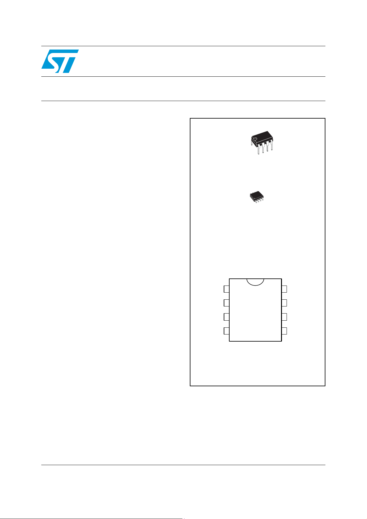
NE555
SA555 - SE555
General purpose single bipolar timers
N
DIP8
(Plastic package)
D
SO8
(Plastic micropackage)
The NE555 monolithic timing circuit is a highly
stable controller capab le of producing accurate
time delays or oscillation. In the time delay mode
of operation, the time is precisely controlled by
one external resistor and capacitor. For a stable
operation as an oscillator, the free running
frequency and the duty cycle are both accurately
controlled with two external resistors and one
capacitor.
The circuit may be triggered and reset on falling
wav eforms, and the output structure can source
or sink up to 200mA.
Pin connections
(top view)
1 - GND
2 - Trigger
3 - Output
4 - Reset
5 - Control voltage
6 - Threshold
7 - Discharge
8 - V
CC
March 2007 Rev 4 1/20
www.st.com
20
Page 2

Contents NE555 - SA555 - SE555
Contents
1 Schematic diagrams . . . . . . . . . . . . . . . . . . . . . . . . . . . . . . . . . . . . . . . . . 3
2 Absolute maximum ratings and operating conditions . . . . . . . . . . . . . 4
3 Electrical characteristics . . . . . . . . . . . . . . . . . . . . . . . . . . . . . . . . . . . . . 5
4 Application information . . . . . . . . . . . . . . . . . . . . . . . . . . . . . . . . . . . . . . 9
4.1 Monostable operation . . . . . . . . . . . . . . . . . . . . . . . . . . . . . . . . . . . . . . . . . 9
4.2 Astable operation . . . . . . . . . . . . . . . . . . . . . . . . . . . . . . . . . . . . . . . . . . . 10
4.3 Pulse width modulator . . . . . . . . . . . . . . . . . . . . . . . . . . . . . . . . . . . . . . . 13
4.4 Linear ramp . . . . . . . . . . . . . . . . . . . . . . . . . . . . . . . . . . . . . . . . . . . . . . . 13
4.5 50% duty cycle oscillator . . . . . . . . . . . . . . . . . . . . . . . . . . . . . . . . . . . . . 14
4.6 Additional information . . . . . . . . . . . . . . . . . . . . . . . . . . . . . . . . . . . . . . . . 15
5 Package information . . . . . . . . . . . . . . . . . . . . . . . . . . . . . . . . . . . . . . . . 16
6 Ordering information . . . . . . . . . . . . . . . . . . . . . . . . . . . . . . . . . . . . . . . 19
7 Revision history . . . . . . . . . . . . . . . . . . . . . . . . . . . . . . . . . . . . . . . . . . . 19
2/20
Page 3
NE555 - SA555 - SE555 Schematic diagrams
T
1 Schematic diagrams
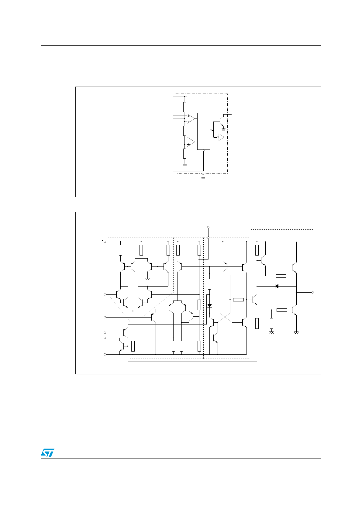
Figure 1. Block diagram
+
V
CC
5kΩ
THRESHOLD
CONTROL VOLTAGE
TRIGGER
COMP
5kΩ
COMP
5kΩ
R
FLIP-FLOP
S
INHIBIT/
RESET
Q
DISCHARGE
OUT
Figure 2. Schematic diagram
THRESHOLD
COMPARATOR
V
HRESHOLD
TRIGGER
RESET
DISCHARGE
G N D
CC
R1
4.7k
Q5 Q6 Q7 Q8 Q9
Q1
Q2
2
4
Q15
7
Q14
1
R2
R3
830
W
W
Q3
R5
10k
4.7k
Q4
Q10
W
RESET
W
R6
100k
Q11 Q12
W
S - 8086
R4
1k
W
Q13
100k
S
CONTROL
VOLTAGE
5
R8
5k
W
Q19
R11
5k
W
R9
5k
W
R7
W
D2
Q16 Q18
Q17
R10
5k
W
4.7k
R17
R12
6.8k
W
Q20
W
Q23
R16
100
Q21
OUTPUT
Q22
R13
3.9k
W
D1
R14
220
R15
4.7k
W
3
W
Q24
W
TRIGGER COMPARATOR FLIP FLOP
3/20
Page 4
Absolute maximum ratings and operating conditions NE555 - SA555 - SE555
2 Absolute maximum ratings and operating conditions
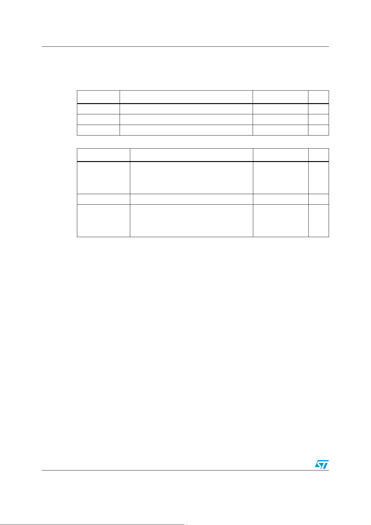
Table 1. Absolute maximum ratings
Symbol Parameter Value Unit
V
CC
T
j
T
stg
Table 2. Operating conditions
Supply voltage 18 V
Junction temperature 150 °C
Storage temperature range -65 to 150 °C
Symbol Parameter Value Unit
Supply voltage
Vth, V
V
trig
CC
, Vcl, V
NE555
SA555
SE555
Maximum input voltage V
reset
4.5 to 16
4.5 to 16
4.5 to 18
CC
Operating free air temperature range
T
oper
NE555
SA555
SE555
0 to 70
-40 to 105
-55 to 125
V
V
°C
4/20
Page 5

NE555 - SA555 - SE555 Electrical characteristics
3 Electrical characteristics
Table 3. T
= +25°C, VCC = +5V to +15V (unless otherwise specified)
amb
Symbol Parameter
Supply current (RL = ∝)
I
Low stage V
CC
High state V
= +5V
CC
VCC = +15V
= 5V
CC
Timing error (monostable)
(R
= 2k to 100kΩ, C = 0.1μF)
A
Initial accuracy
(1)
Drift with temperature
Drift with supply voltage
Timing error (astable)
(R
= 1kΩ to 100kΩ, C = 0.1μF, VCC = +15V)
A, RB
Initial accuracy -
(1)
Drift with temperature
Drift with supply voltage
Control voltage level
V
CL
VCC = +15V
= +5V
V
CC
Threshold voltage
V
th
V
CC
= +15V
VCC = +5V
Threshold current
I
th
(2)
Trigger voltage
V
V
I
trig
reset
trig
VCC = +15V
= +5V
V
CC
Trigger current (V
Reset voltage
(3)
= 0V) 0.5 0.9 0.5 2.0 µA
trig
Reset current
I
reset
V
V
reset
reset
= +0.4V
= 0V
Low level output voltage
= +15VI
V
CC
V
OL
VCC = +5V I
O(sink)
I
O(sink)
I
O(sink)
I
O(sink)
O(sink)
I
O(sink)
= 10mA
= 50mA
= 100mA
= 200mA
= 8mA
= 5mA
High level output voltage
V
= +15VI
V
OH
CC
V
CC
= +5V I
O(sink)
I
O(sink)
O(sink)
= 200mA
= 100mA
= 100mA
SE555 NE555 - SA555
Min. Typ. Max. Min. Typ. Max.
3
10
2
0.5
30
0.05
1.5
90
0.15
9.6
2.9103.33
9.4
2.7103.33
5
12
3
10
2
2
100
0.2
1
50
0.130.5
2.25
150
0.3
10.4
3.892.6103.33114
10.648.8
2.4103.33
6
15
ppm/°C
ppm/°C
11.2
4.2
0.1 0.25 0.1 0.25 µA
4.8
1.4551.67
5.2
1.9
4.5
1.151.67
5.6
2.2
0.4 0.7 1 0.4 0.7 1 V
13
0.1
0.4
0.1
0.4
2.5
0.1
0.05
12.5
13.3
3
3.3
0.4
1
0.15
0.5
2
2.2
0.1
0.4
0.1
0.4
2
0.4
1.5
0.25
0.75
2.5
2.5
0.25
0.2
0.3
0.25
0.4
0.35
12.5
12.75
2.75
13.3
3.3
Unit
mA
%
%/V
%
%/V
V
V
V
mA
V
V
5/20
Page 6
Electrical characteristics NE555 - SA555 - SE555
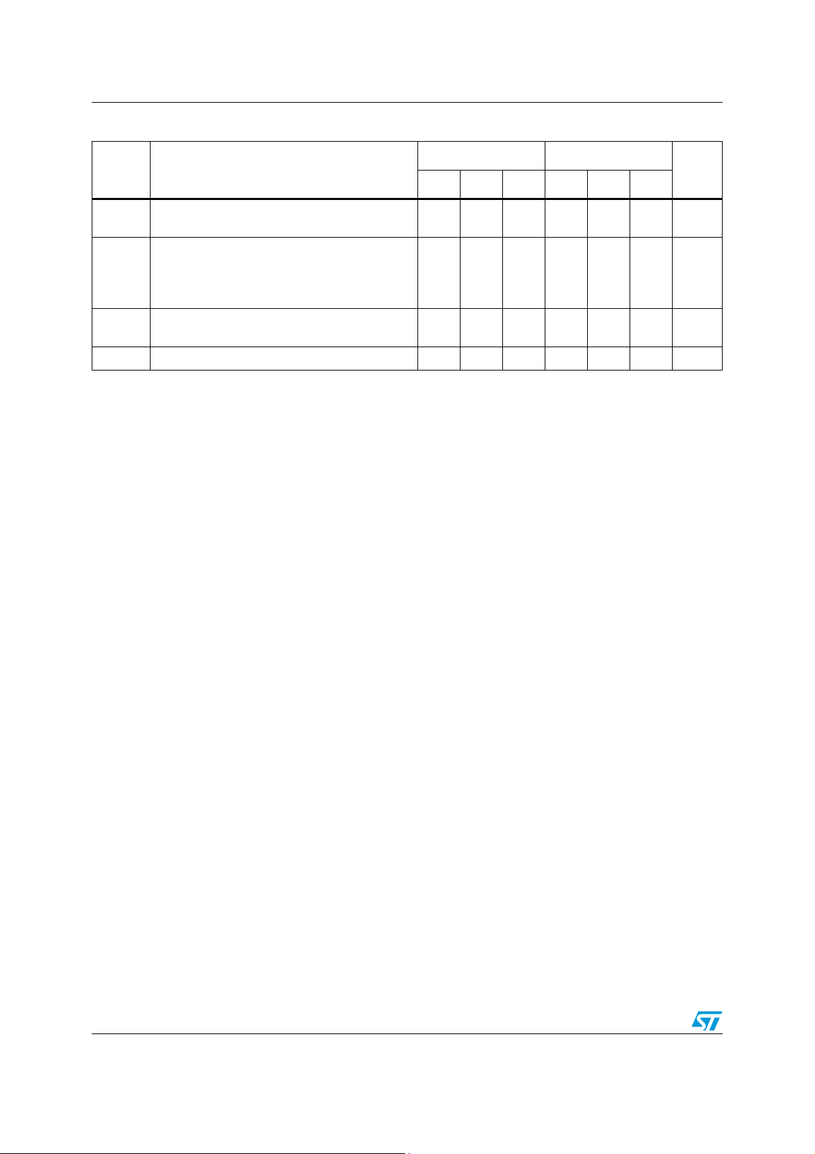
Table 3. T
= +25°C, VCC = +5V to +15V (unless otherwise specified)
amb
SE555 NE555 - SA555
Symbol Parameter
Min. Typ. Max. Min. Typ. Max.
I
dis(off)
V
dis(sat)
t
1. Tested at VCC = +5V and VCC = +15V.
2. This will determine the maximum value of R
operation and 3.5MΩ for +5V operation.
3. Specified with trigger input high.
4. No protection against excessive pin 7 current is necessary, providing the package dissipation rating is not exceeded.
5. Time measured from a positive pulse (from 0V to 0.8xV
Output pin. Trigger is tied to Threshold.
Discharge pin leakage current
(output high) V
Discharge pin saturation voltage
(output low)
VCC = +15V, I
VCC = +5V, I
t
Output rise time
r
t
Output fall time
f
Turn off time
off
(4)
(5)
dis
dis
dis
(V
= 10V
= 15mA
= 4.5mA
= VCC)0.50.5µs
reset
+ RB for 15V operation. The maximum total (RA + RB) is 20MΩ for 15V
A
) on the Threshold pin to the transition from high to low on the
CC
20 100 20 100 nA
18080480
200
100
100
200
200
18080480
200
100
100
300
300
Unit
mV
ns
6/20
Page 7
NE555 - SA555 - SE555 Electrical characteristics
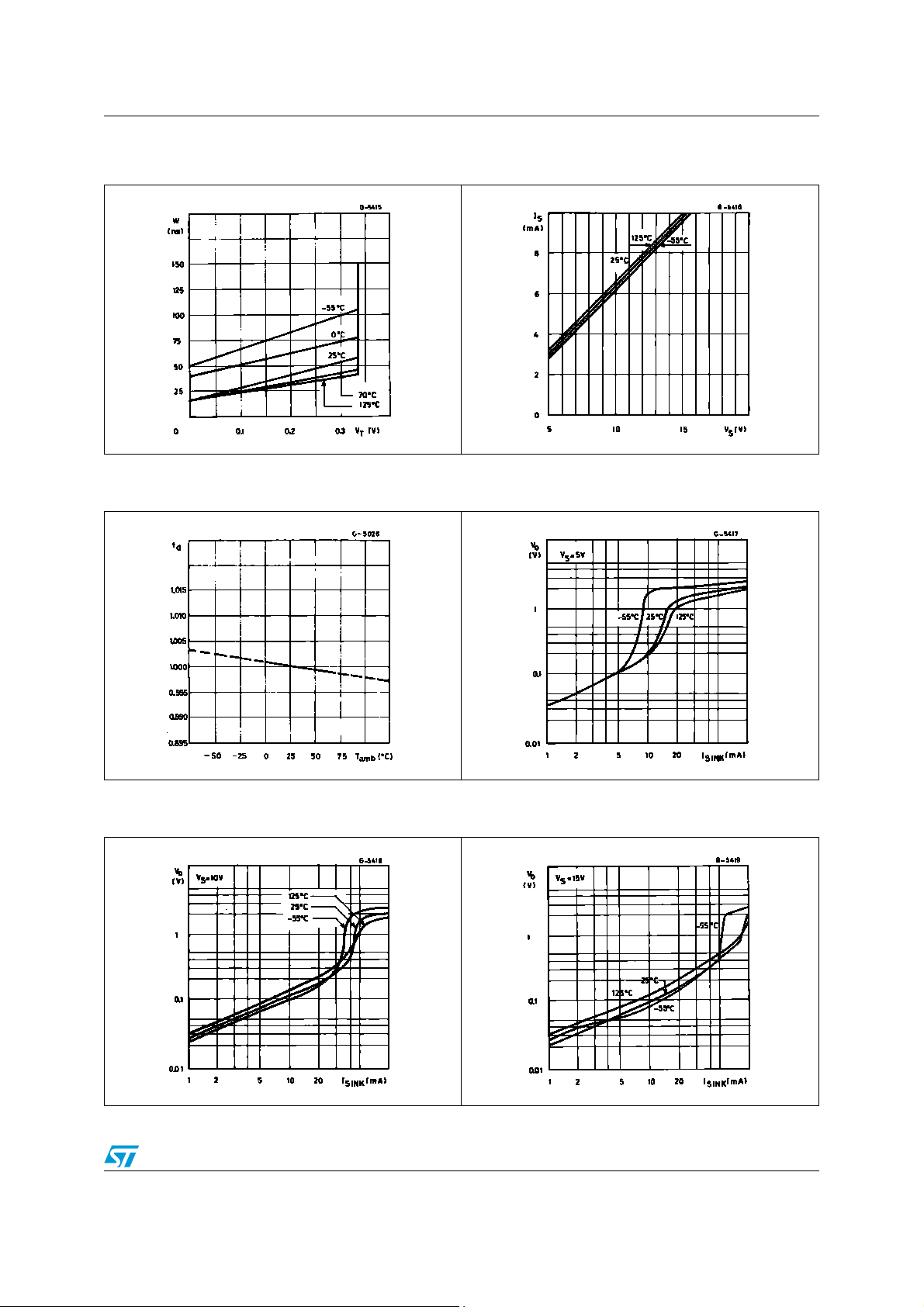
Figure 3. Minimum pulse width required for
triggering
Figure 4. Supply current versus supply
voltage
Figure 5. Delay time versus temperature Figure 6. Low output voltage versus output
sink current
Figure 7. Low output voltage versus output
sink current
Figure 8. Low output voltage versus output
sink current
7/20
Page 8
Electrical characteristics NE555 - SA555 - SE555
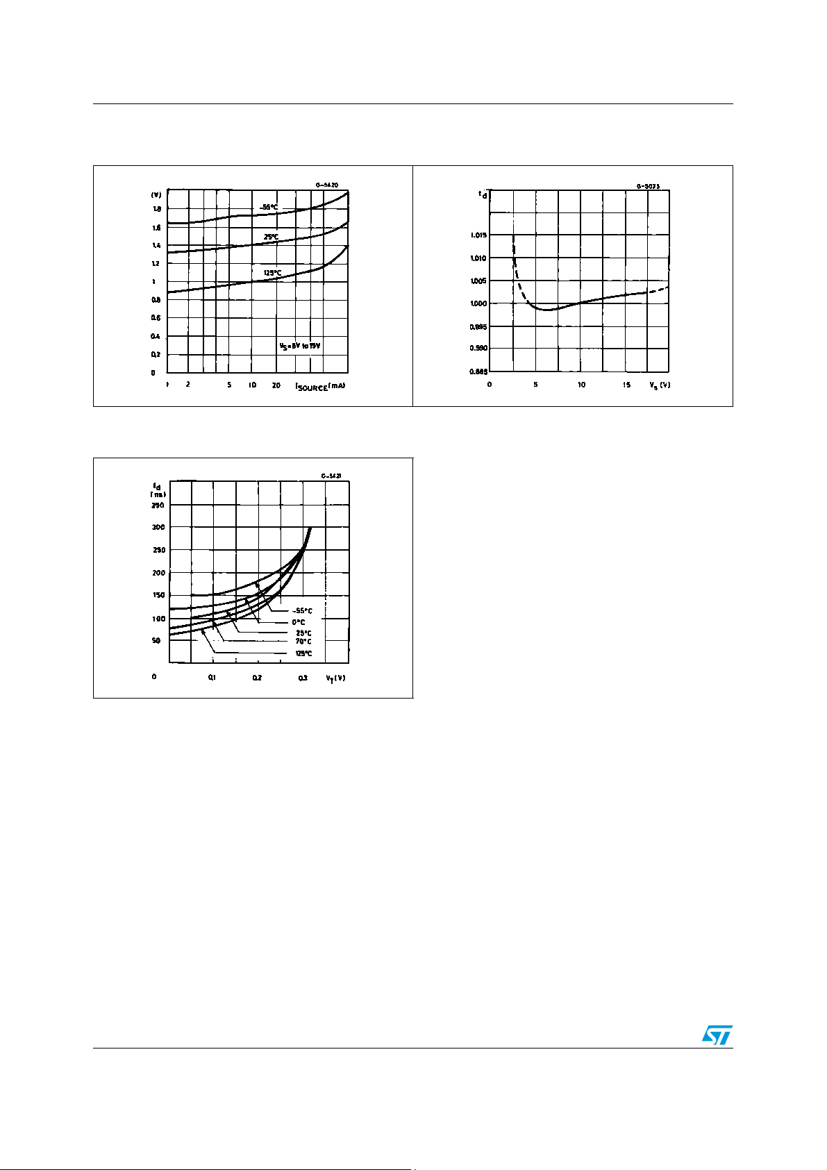
Figure 9. High output voltage drop versus
output
Figure 11. Propagation delay versus voltage
level of trigger value
Figure 10. Delay time versus supply voltage
8/20
Page 9
NE555 - SA555 - SE555 Application information
4 Application information
4.1 Monostable operation
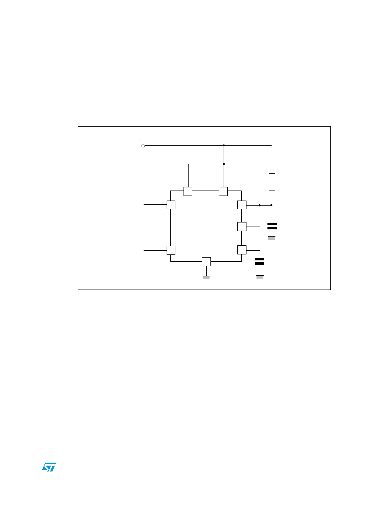
In the monostable mode, the timer generates a single pulse. As shown in Figure 12, the
external capacitor is initially held discharged by a transistor inside the timer.
Figure 12. Typical schematics in monostable operation
V
= 5 to 15V
CC
Reset
R1
4
8
Trigger
Output
The circuit triggers on a negative-going input signal when the level reaches 1/3 V
2
NE555
3
1
7
6
Control Voltage
5
0.01
C1
μF
. Once
CC
triggered, the circuit remains in this state until the set time has elapsed, e v en if it is triggered
again during this interval. The duration of the output HIGH state is given by t = 1.1 R
1C1
and
is easily determined by Figure 14.
Note that because the charge rate and the threshold level of the comparator are both
directly proportional to supply voltage, th e ti ming int e rval is inde pende nt of sup ply. Applying
a negative pulse simultaneously to the reset terminal (pin 4) and the trigger terminal (pin 2)
during the timing cycle discharges the external capacitor and causes the cycle to start over.
The timing cycle now starts on the positive edge of the reset pulse. During the time the reset
pulse is applied, the output is driven to its LOW state.
When a negative trigger pulse is applied to pin 2, the f lip-flop is set, releasing the shortcircuit across the external capacitor and driving the output HIGH. The voltage across the
capacitor increases exponentially with the time co nsta nt t = R
the capacitor equals 2/3 V
, the comparator resets the flip-flop which then discharges the
CC
. When the voltage across
1C1
capacitor rapidly and drives the output to its LOW state.
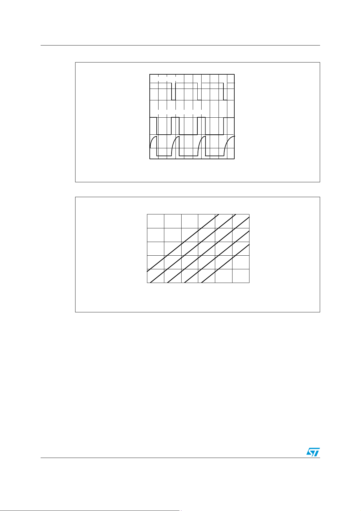
Figure 13 shows the actual waveforms generated in this mode of operation.
When Reset is not used, it should be tied high to avoid any possibility of unwanted
triggering.
9/20
Page 10
Application information NE555 - SA555 - SE555
CAPACITOR VOLTAGE = 2.0V/div
t = 0.1 ms / div
INPUT = 2.0V/div
OUTPUT VOLTAGE = 5.0V/div
R1 = 9.1kΩ, C1 = 0.01μF, R = 1kΩ
L
C
(μF)
10
1.0
0.1
0.01
0.001
10 100 1.0 10 100 10 (t )
d
μs μs
ms ms ms s
10M
Ω
1M
Ω
1
00
k
Ω
10k
Ω
R1
=
1k
Ω
Figure 13. Waveforms in monostable operation
Figure 14. Pulse duration versus R1C1
4.2 Astable operation
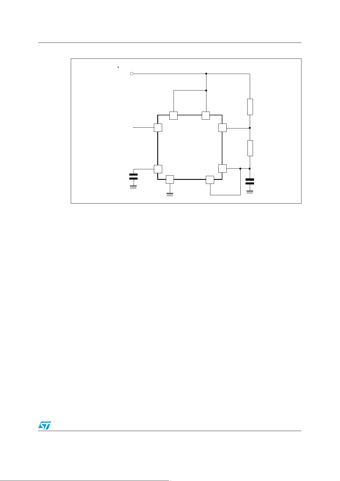
When the circuit is connected as shown in Figure 15 (pin 2 and 6 connected) it triggers itself
and free runs as a multi-vibrator. The external capacitor charges through R
discharges through R
of these two resistors.
In the astable mode of oper ation, C
As in the triggered mode, the charge and discharge times and, therefore, frequency are
independent of the supply voltage.
10/20
and R2 and
only. Thus the duty cycle can be set accurately by adjusting the ratio
2
charges and discharges between 1/3 VCC and 2/3 VCC.
1
1
Page 11
NE555 - SA555 - SE555 Application information
Figure 15. Typical schematics in astable operation
= 5 to 15V
V
CC
R1
4
8
Output
0.01μF
Control
Voltage
3
NE555
5
1
7
R2
6
2
C1
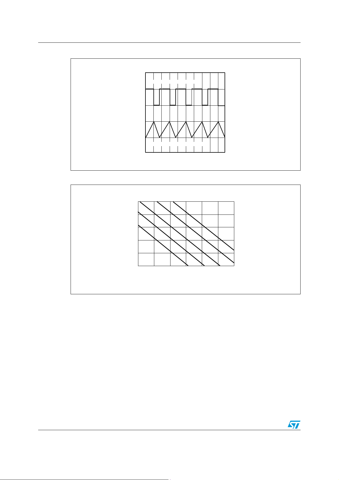
Figure 16 shows the actual waveforms generated in this mode of operation.
The charge time (output HIGH) is given by:
t1 = 0.693 (R
+ R2) C
1
1
and the discharge time (output LOW) by:
t2 = 0.693 (R
2
) C
1
Thus the total period T is given by:
T = t1 + t2 = 0.693 (R1 + 2R2) C1
The frequency of oscillation is then:
f =
1
---
T
1.44
-------------------------------------- -=
R1 2R2+()C1
It can easily be found from Figure 17.
The duty cycle is given by:
------------------------- -=
R1 2R2+
R2
D
11/20
Page 12
Application information NE555 - SA555 - SE555
t = 0.5 ms / div
OUTPUT VOLTAGE = 5.0V/div
CAPACITOR VOLTAGE = 1.0V/div
R1 = R2 = 4.8kΩ, C1= 0.1μF, R = 1kΩ
L
C
(μF)
10
1.0
0.1
0.01
0.001
0.1 1 10 100 1k 10k f (Hz)
o
1
M
Ω
R
1
+
R
2
=
1
0
M
Ω
1
0
0
k
Ω
1
0
k
Ω
1
k
Ω
Figure 16. Waveforms in astable operation
Figure 17. Free running frequency versus R
, R2 and C
1
1
12/20
Page 13
NE555 - SA555 - SE555 Application information
Trigger
Output
C
NE555
2
4
3
1
5
6
7
8
E
V
CC
0.01μF
R2
R1
R
2N4250
or equiv.
4.3 Pulse width modulator
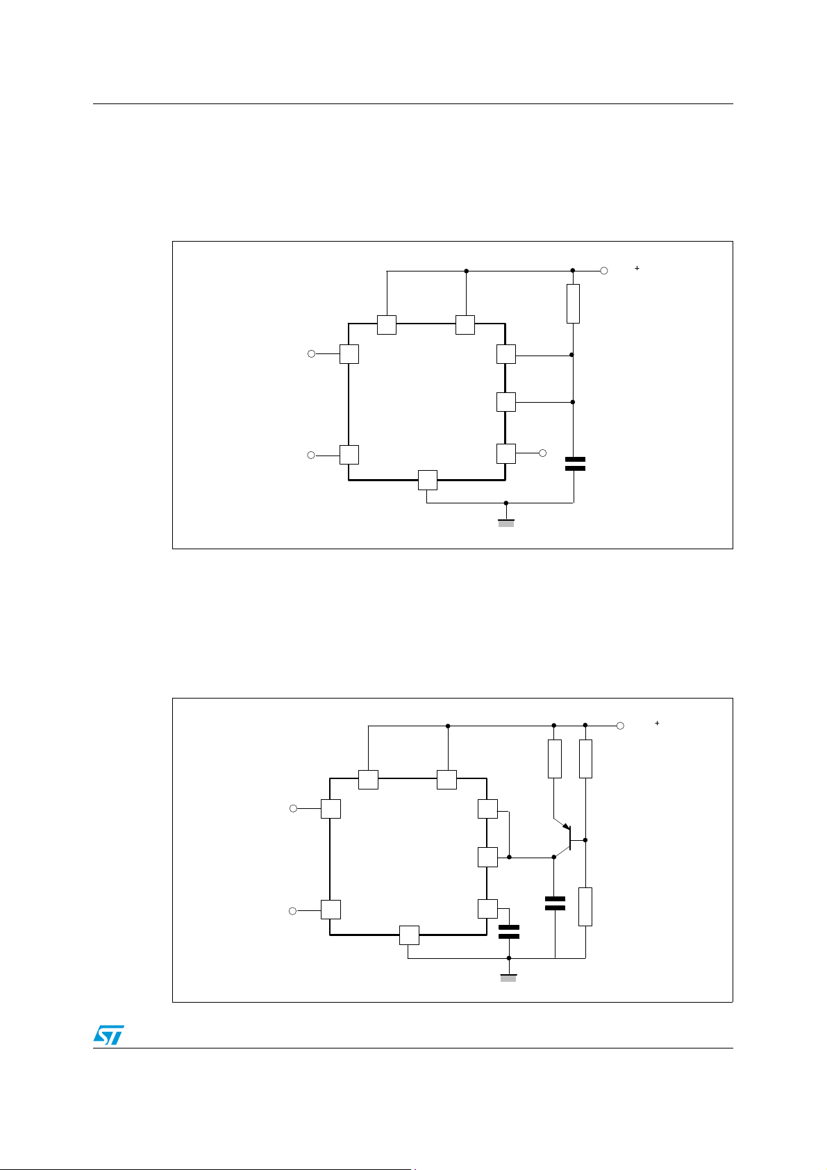
When the timer is connected in the monostab le mode a nd triggered with a cont inuous pulse
train, the output pulse width can be m odulated by a signal applied to pin 5. Figure 18 shows
the circuit.
Figure 18. Pulse width modulator
V
CC
R
A
4
8
Trigger
Output
4.4 Linear ramp
When the pull-up resistor, RA, in the monostable circuit is replaced by a constant current
source, a linear ramp is generated. Figure 19 shows a circuit configuration that will perform
this function.
Figure 19. Linear ramp
2
NE555
3
1
7
6
Modulation
Input
5
C
13/20
Page 14
Application information NE555 - SA555 - SE555
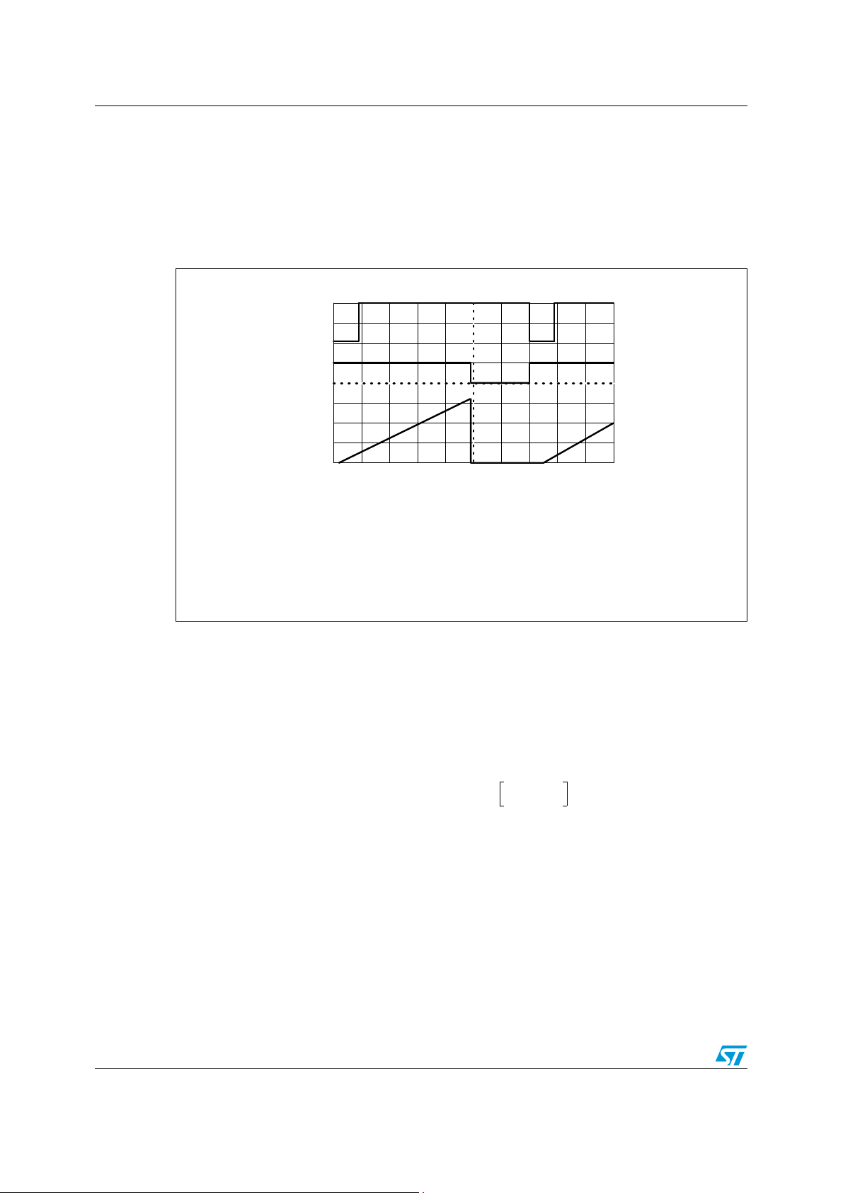
Figure 20 shows the waveforms generator by the linear ramp.
The time interval is given by:
(2/3 Vcc RE (R1+R2) C
--------------------------------------------------------------- -
T =
R1 Vcc - VBE (R1+R2)
VBE = 0.6V
Figure 20. Linear ramp
V
= 5V
CC
Time:
20µs/DIV
+ 47kΩ
R
1
R2 = 100kΩ
= 2.7kΩ
R
E
C = 0.01µF
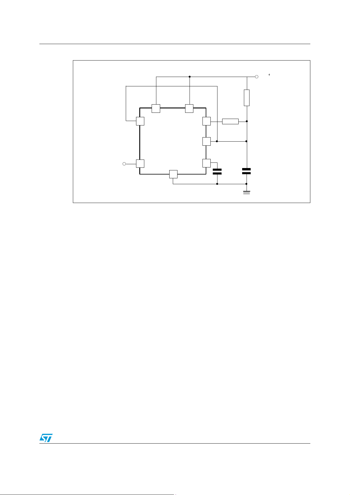
4.5 50% duty cycle oscillator
For a 50% duty cycle, the resistors RA and RE can be connected as in figure 19. The time
period for the output hi gh is th e sam e a s for astable operation (see Section 4.2 on page 10):
t1 = 0.693 R
For the output low it is
Thus the frequency of oscillation is:
C
A
t2[(R. RB)/(RA+RB)].C.Ln
=
Top trace: input 3V/DIV
Middle trace: output 5V/DIV
Bottom trace: output 5V/DIV
Bottom trace: capacitor voltage 1V/DIV
RB 2RA–
-------------------------- -
2RB RA–
1
f
---------------- -=
t1 t2+
14/20
Page 15
NE555 - SA555 - SE555 Application information
Figure 21. 50% duty cycle oscillator
V
CC
4
2
8
R
7
B
22kΩ
R
A
51kΩ
V
CC
Out
3
Note that this circuit will not oscillate if R
and R
cannot bring pin 2 down to 1/3 VCC and trigger the lower comparator.
B
4.6 Additional information
Adequate power supply by passing is necessary to protect associated circuitry. The
minimum recommended is 0.1µF in parallel with 1µF electrolytic.
NE55
1
is greater than 1/2 RA because the junction of RA
B
6
5
0.01μF
C
0.01μF
15/20
Page 16

Package information NE555 - SA555 - SE555
5 Package information
In order to meet environmental requirements, STMicroelectronics offers these devices in
ECOPACK
category of second level interconnect is marke d on the pa ckage and on the inner box label,
in compliance with JEDEC Standard JESD97. The maximum ratings related t o soldering
conditions are also marked on the inner box label. ECOPACK is an STMicroelectronics
trademark. ECOPACK specifications are available at: www.st.com
®
packages. These packages have a lead-free second level interconnect. The
.
16/20
Page 17
NE555 - SA555 - SE555 Package information
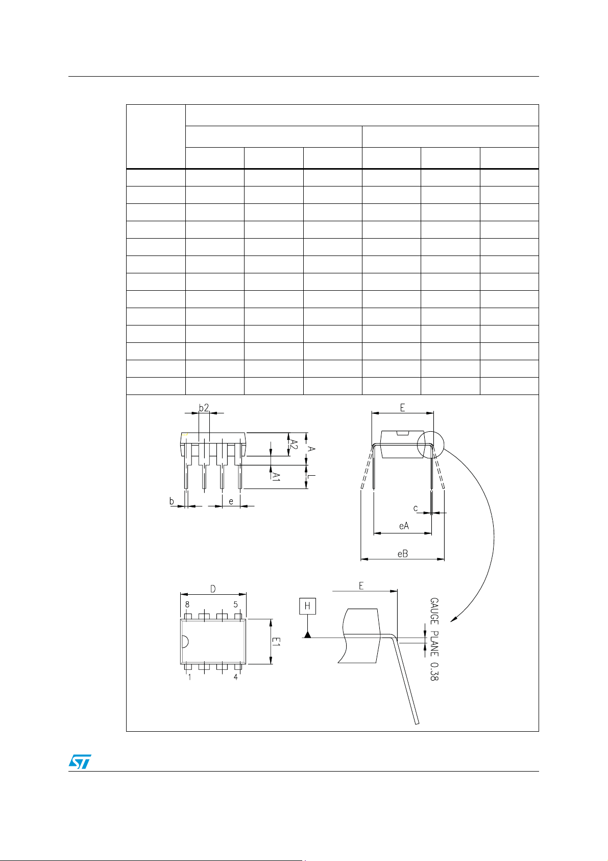
Figure 22. DIP8 package mechanical data
Dimensions
Ref.
Min. Typ. Max. Min. Typ. Max.
A5.330.210
A1 0.38 0.015
A2 2.92 3.30 4.95 0.115 0.130 0.195
b 0.36 0.46 0.56 0.014 0.018 0.022
b2 1.14 1.52 1.78 0.045 0.060 0.070
c 0.20 0.25 0.36 0.008 0.010 0.014
D 9.02 9.27 10.16 0.355 0.365 0.400
E 7.62 7.87 8.26 0.300 0.310 0.325
E1 6.10 6.35 7.11 0.240 0.250 0.280
e 2.54 0.100
eA 7.62 0.300
eB 10.92 0.430
L 2.92 3.30 3.81 0.115 0.130 0.150
Millimeters Inches
17/20
Page 18
Package information NE555 - SA555 - SE555
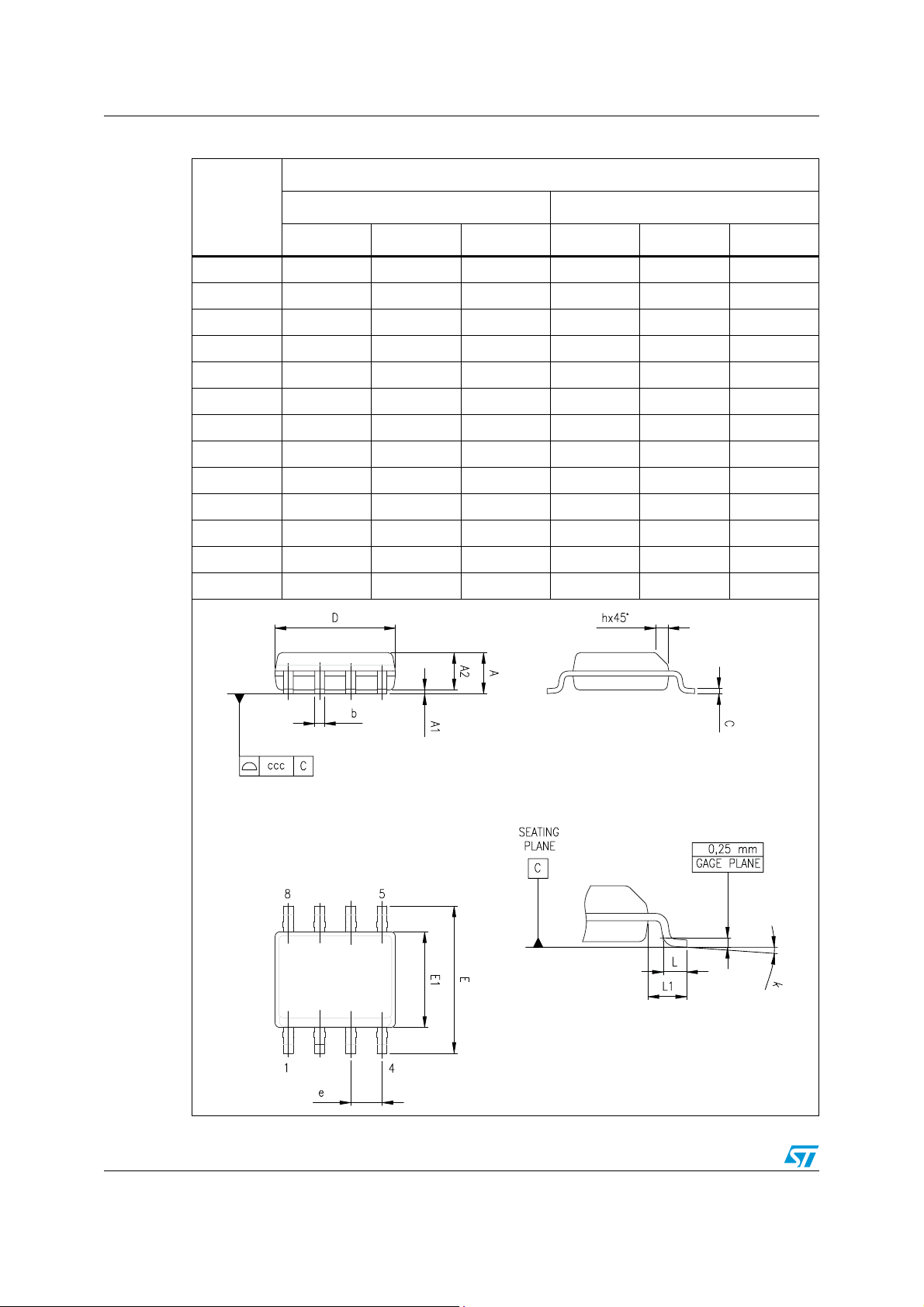
Figure 23. SO8 package mechanical data
Dimensions
Ref.
Min. Typ. Max. Min. Typ. Max.
A1.750.069
A1 0.10 0.25 0.004 0.010
A2 1.25 0.049
b 0.28 0.48 0.011 0.019
c 0.17 0.23 0.007 0.010
D 4.80 4.90 5.00 0.189 0.193 0.197
H 5.80 6.00 6.20 0.228 0.236 0.244
E1 3.80 3.90 4.00 0.150 0.154 0.157
e 1.27 0.050
h 0.25 0.50 0.010 0.020
L 0.40 1.27 0.016 0.050
k1°8°1°8°
ccc 0.10 0.004
Millimeters Inches
18/20
Page 19
NE555 - SA555 - SE555 Ordering information
6 Ordering information
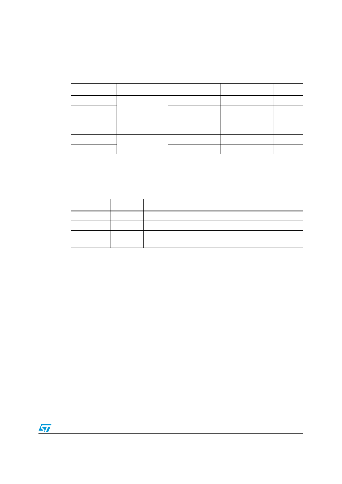
Table 4. Order codes
Part number Temperature range Package Packing Marking
NE555N
0°C, +70°C
NE555D/DT SO8 Tube or tape & reel NE555
SA555N
-40°C, +105°C
SA555D/DT SO8 Tube or tape & reel SA555
SE555N
-55°C, + 125°C
SE555D/DT SO8 Tube or tape & reel SE555
7 Revision history
Date Revision Changes
1-Jun-2003 1 Initial release.
2004-2006 2-3 Internal revisions
15-Mar-2007 4
DIP8 Tube NE555N
DIP8 Tube SA555N
DIP8 Tube SE555N
Expanded order code table.
Template update.
19/20
Page 20

NE555 - SA555 - SE555
Please Read Carefully:
Information in this document is provided solely in connection with ST products. STMicroelectronics NV and its subsidiaries (“ST”) reserve the
right to make changes, corrections, modifications or improvements, to this document, and the products and services described herein at any
time, without notice.
All ST products are sold pursuant to ST’s terms and conditions of sale.
Purchasers are solely res ponsibl e fo r the c hoic e, se lecti on an d use o f the S T prod ucts and s ervi ces d escr ibed he rein , and ST as sumes no
liability whatsoever relati ng to the choice, selection or use of the ST products and service s described herein.
No license, express or implied, by estoppel or otherwise, to any intellectual property rights is granted under this document. If any part of this
document refers to any third pa rty p ro duc ts or se rv ices it sh all n ot be deem ed a lice ns e gr ant by ST fo r t he use of su ch thi r d party products
or services, or any intellectua l property c ontained the rein or consi dered as a warr anty coverin g the use in any manner whats oever of suc h
third party products or servi ces or any intellectual property contained therein.
UNLESS OTHERWISE SET FORTH IN ST’S TERMS AND CONDITIONS OF SALE ST DISCLAIMS ANY EXPRESS OR IMPLIED
WARRANTY WITH RESPECT TO THE USE AND/OR SALE OF ST PRODUCTS INCLUDING WITHOUT LIMITATION IMPLIED
WARRANTIES OF MERCHANTABILITY, FITNESS FOR A PARTICUL AR PURPOS E (AND THEIR EQUIVALE NTS UNDER THE LAWS
OF ANY JURISDICTION), OR INFRINGEMENT OF ANY PATENT, COPYRIGHT OR OTHER INTELLECTUAL PROPERTY RIGHT.
UNLESS EXPRESSLY APPROVED IN WRITING BY AN AUTHORIZED ST REPRESENTATIVE, ST PRODUCTS ARE NOT
RECOMMENDED, AUTHORIZED OR WARRANTED FOR USE IN MILITARY, AIR CRAFT, SPACE, LIFE SAVING, OR LIFE SUSTAINING
APPLICATIONS, NOR IN PRODUCTS OR SYSTEMS WHERE FAILURE OR MALFUNCTION MAY RESULT IN PERSONAL INJ URY,
DEATH, OR SEVERE PROPERTY OR ENVIRONMENTAL DAMAGE. ST PRODUCTS WHICH ARE NOT SPECIFIED AS "AUTOMOTIVE
GRADE" MAY ONLY BE USED IN AUTOMOTIVE APPLICATIONS AT USER’S OWN RISK.
Resale of ST products with provisions different from the statements and/or technical features set forth in this document shall immediately void
any warranty granted by ST fo r the ST pro duct or serv ice describe d herein and shall not cr eate or exten d in any manne r whatsoever , any
liability of ST.
ST and the ST logo are trademarks or registered trademarks of ST in various countries.
Information in this document su persedes and replaces all information previously supplied.
The ST logo is a registered trademark of STMicroelectronics. All other names are the property of their respective owners.
© 2007 STMicroelectronics - All rights reserved
STMicroelectronics group of compan ie s
Australia - Belgium - Brazil - Canada - China - Czech Republic - Finland - France - Germany - Hong Kong - India - Israel - Italy - Japan -
Malaysia - Malta - Morocco - Singapore - Spain - Sweden - Switzerland - United Kingdom - United States of America
www.st.com
20/20
 Loading...