

Page 1
S DM9926
S amHop Microelec tronics C orp.
Augus t , 2002
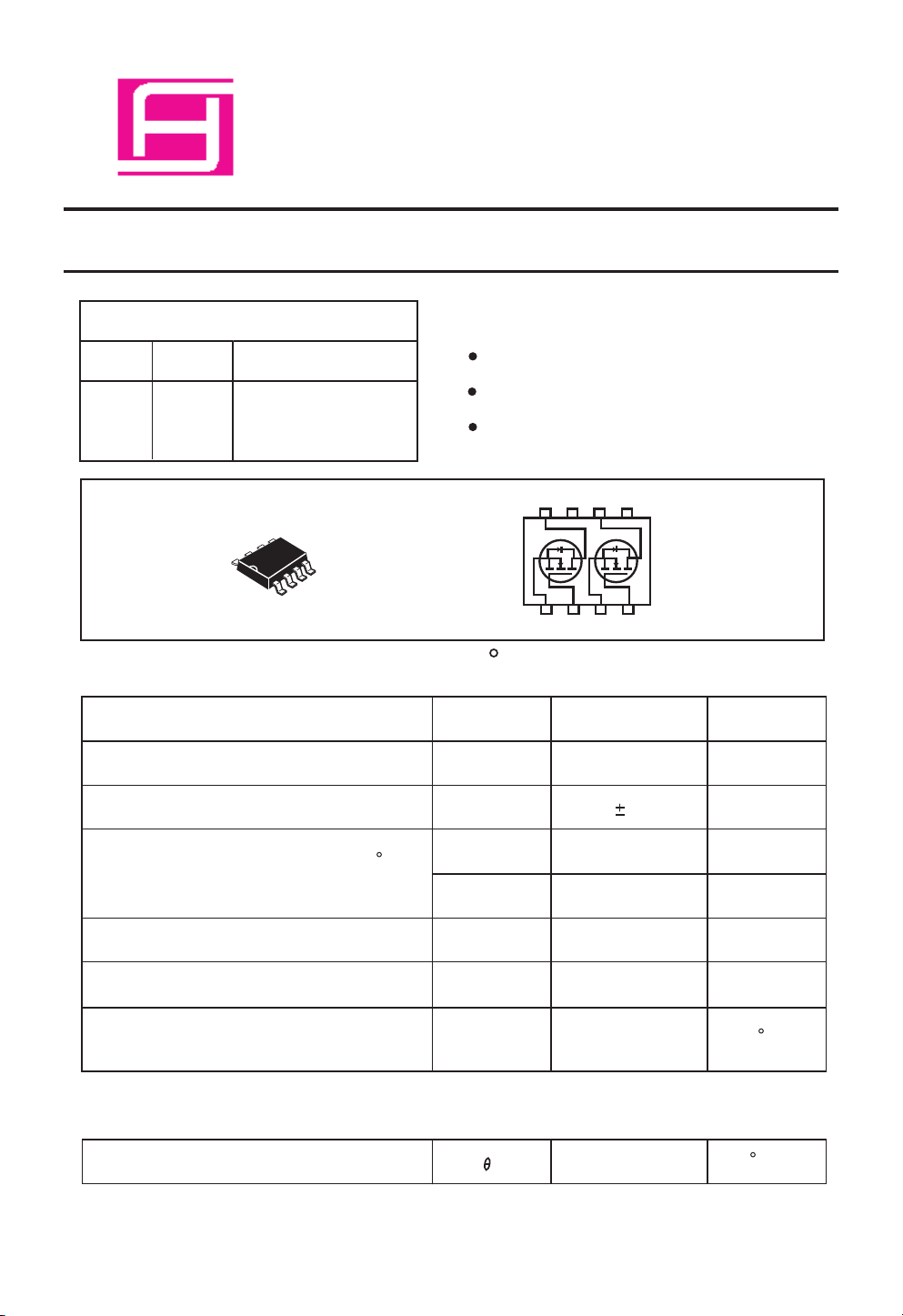
Dual N-C hannel E nhancement Mode Field E ffect T ransis tor
PR ODUC T S UMMAR Y
VDS S
20V
ID
6A
R DS (O N) ( m
30 @ VGS = 4.5V
32 @ VGS = 4.0V
40 @ VGS = 2.7V
S O-8
1
W
) Max
ABS OLUT E MAX IMUM R ATINGS (TA=25 C unless otherwis e noted)
F E ATUR E S
S uper high dense cell design for low R
R ugged and reliable.
S urface Mount P ackage.
D1 D1 D2 D2
8 7 6 5
1 2 3 4
S 1 G 1 S 2 G 2
DS (O N
).
P arameter
Drain-S ource Voltage
G ate-S ource Voltage
Drain C urrent-C ontinuous @ TJ=125 C
-P uls ed
Drain-S ource Diode F orward C urrent
Maximum P ower Dis s ipation
a
b
(300us Puls e Width)
a
a
Opera ting J unction a nd S torage
Temperature R ange
THE R MAL C HAR AC T E R IS T IC S
Thermal R es is tance, J unction-to-Ambient
S ymbol
V
DS
V
G S
I
D
I
DM
I
S
P
D
TJ, T
S TG
a
R
J A
Limit Unit
20
12
6.0
35
1.7
2
-55 to 150
62.5
V
V
A
A
A
W
C
C
/W
1
Page 2
S DM9926
E LE C T R IC AL C HAR AC TE R IS T IC S (T A 25 C unles s otherwis e noted)
P arameter
S ymbol
=
C ondition
Min
Typ
C
OF F C HAR AC TE R IS TICS
V
G S
Drain-S ource Breakdown Voltage
Zero G ate Voltage Drain C urrent
G ate-B ody Leakage
ON C HAR AC TE R IS TIC S
b
G ate Threshold Voltage
Drain-S ource On-S tate R es istance
On-S tate Drain C urrent
DYNAMIC C HAR AC TE R IS TIC S
0V, ID 250uA
B V
DS S
I
DS S
I
G S S
V
G S (th)
R
DS (ON)
I
D(ON)
g
F S
c
VDS 20V, V
V
G S
V
DS VG S
V
G S
V
G S
V
G S
V
DS
V
DS
=
=
= =
=
=
G S
8V,V
DS
=
, ID = 250uA
=
4.5V, I
D
=
4.0V, I
D
=
=
= 5V, V
= =
2.7V, I
10V, I
D
G S
D
=
0V
0V
=
6.0A
6.0A
5.2A
= 4.5V
6.0A
20
20
1.1
28
29
36
17
Max
1
100
30
32
40
Unit
V
uA
nA
V
m ohm
A
SF orward Trans conductance
Input C apacitance
Output C apacitance
R evers e Trans fer C apacitance
S WIT C HING C HAR AC T E R IS TICS
Turn-O n Delay Time
R ise Time
Turn-O ff Delay Time
F a ll Time
Total G ate C harge
G ate-S ource C harge
G ate-Drain C harge
C
IS S
V
DS
=8V, V
G S
= 0V
C
OS S
C
R S S
c
t
D(ON)
t
r
t
D(OFF)
t
f
Q
g
f =1.0MH
VDD = 10V,
ID = 1A,
V
G E N
= 4.5V,
RL = 10
R
GE N
ohm
= 6
Z
ohm
710
300
80
10
15 30
26
20 40
12
P
P
P
20 ns
ns
ns
50
ns
nC
15
F
F
F
VDS =10V, ID = 6A,
Q
Q
gs
gd
2
V
G S
=4.5V
4
2
nC
nC
Page 3

S DM9926
E LE C T R IC AL C HAR AC TE R IS T IC S (TA=25 C unles s otherwis e noted)
P a rameter
S ymbol
C ondition
Min
Typ
C
Max
Unit
5
DR AIN-S OUR C E DIODE C HAR AC T E R IS TIC S
Diode F orwa rd Volta ge
V
S D
b
V
G S
= 0V, Is =1.7A
0.72
1.2
V
Notes
a.S urface Mounted on F R 4 B oard, t 10s ec.
b.Puls e Test:P uls e W idth 300us , Duty C ycle 2%.
c.G uaranteed by design, not subject to production tes ting.
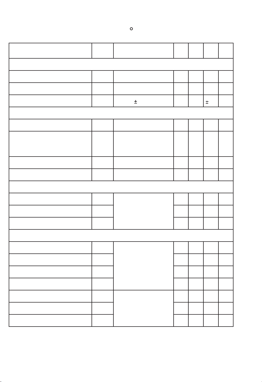
25
VGS =4.5,3. 5,2.5V
20
15
10
5
ID, Drain Current(A)
0
0 1 2 3 4 5 6
VDS , Drain-to-S ource Voltage (V)
VGS =1.5V
F igure 1. Output C haracteris tics
25
20
15
10
T j=12 5 C
5
ID, Dra in C urrent ( A)
0
0. 0 0. 5 1 1.5 2 2.5 3
VGS , G ate-to-S ource Volta ge (V )
25 C
F igure 2. Trans fer C hara cteristics
-55 C
300 0
250 0
200 0
150 0
100 0
C , C apa cita nce (pF )
500
0
0 2 4 6 8 10 12
VDS , Drain-to S ource Voltage ( V)
F igure 3. Capa citance
C iss
C oss
C rss
0. 06
VGS =4.5V
0. 05
0. 04
0. 03
0. 02
On-R esistanc e(Ohms)
0. 01
R DS (O N),
0. 00
0 5 10 15 20
ID, Dra in C urrent(A)
T j=12 5 C
25 C
-55 C
F igure 4. On-R esistance Va riation with
Drain C urrent and Temperature
3
Page 4

S DM9926
1.09
VDS=V
1.06
1.03
1.00
0.97
Vth, N ormalized
0.94
0.91
G ate-S ource T hreshold Voltage
-50 -25 0 25 50 75 1 00 125 150
Tj, Junction T emperature ( C )
G S
ID=250uA
F igure 5. Gate T hreshold V ariation
with Temperature
36
30
24
18
12
6
gFS , T ransconductance (S )
0
0 3 6 9 12 15
VDS=10V
1.15
1.10
1.05
1.00
0.95
0.90
B VDS S, Normalized
0.85
Dra in-S ource B rea kdown V oltage
ID=250uA
-50 -25 0 25 50 75 100 125 150
Tj, Junction T emperature ( C )
F igure 6. Brea kdown Voltage V ariation
with Temperature
20
10
1
Is , S ource-drain current ( A)
0
0.4 0.6 0.8 1.0 1.2 1.4
TJ=25 C
5
IDS , Drain-S ource C urrent (A)
F igure 7. Trans conductance V ariation
with Dra in Current
5
VDS=10V
4
ID=6A
3
2
1
VGS , G ate to S ource V oltage (V )
0
0 2 4 6 8 10 12 14
Qg, Total G ate C harge (nC)
16
F igure 9. Gate C harge
VS D, Body Diode F orward Voltage (V)
F igure 8. Body Diode F orward V oltage
Variation with S ource C urrent
50
10
(O N) L imit
DS
R
1
1
V
G S
0.1
ID, Dra in C urrent (A )
0.03
=4.5V
S ingle P ulse
Tc=25 C
0.1 1 10 20 50
VDS , Drain-S ource Voltage ( V)
10ms
100 ms
1s
DC
F igure 10. Ma ximum S afe
Operating Area
4
Page 5

S DM9926
DD
V
on
t
d(off)
t
r
d(on)
R
5
V
G S
IN
V
G EN
R
G
L
D
OU T
V
S
t
OU T
V
IN
V
10%
t
90%
10% 10%
INVE R T E D
50% 50%
P ULS E W IDT H
90%
t
off
f
t
90%
F igure 11. S witching T est Circuit
2
1
Duty C yc le=0.5
0. 2
0. 1
0. 1
0. 05
0. 01
0. 02
S ingle P ulse
-4
10
-3
10
r(t), Norma lized E ffective
T rans ient Thermal Impedance
F igure 13. Normalized Therma l Trans ient Impedance C urve
F igure 12. S witching Waveforms
-2
10
S quare W ave P ulse Dura tion (s ec)
-1
10
DM
P
1
t
2
t
1. R thJA ( t) =r (t) * R JA
th
2. R J A=S ee Data shee t
3. TJ M-T A = PDM* R J A ( t)
4. Duty C ycle , D=t1/t2
1 10 100
th
th
5
 Loading...