

Page 1
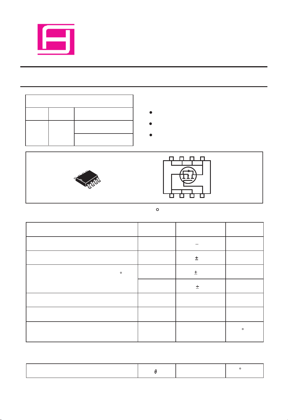
S DM9433
S amHop Microelectronics C orp.
P -C hannel E nhancement Mode MOS F E T
PR ODUC T S UMMAR Y
VDS S
-20V
ID
-5. 4A
R DS (O N) ( m
45 @ VG S = -4.5V
70 @ VG S = -2.7V
S O-8
1
W
) MAX
AB S OLUT E MAX IMUM R ATING S (TA=25 C unles s otherwise noted)
F E AT U R E S
S uper high dens e cell des ign for low R
R ugged and reliable.
S urface Mount P ackage.
D D D D
8 7 6 5
1 2 3 4
S S S G
March , 2003
DS (O N
).
P arameter
Drain-S ource Voltage
G ate-S ource Voltage
Drain C urrent-Continuous @ TJ=125 C
-P ulsed
Drain-S ource Diode F orward C urrent
Maximum P ower Dis sipation
a
b
a
a
Operating J unction and S torage
Tempera ture R ange
THE R MAL C HAR AC TE R IS TIC S
Thermal R esis tance, J unction-to-Ambient
S ymbol
V
DS
V
G S
I
D
I
DM
I
S
P
D
TJ, T
S TG
a
R
J A
Limit Unit
20
12
5.4
20
2.6
2.5
-55 to 150
50
V
V
A
A
A
W
C
C
/W
1
Page 2
S DM9433
E LE C T R IC AL C HAR AC TE R IS T IC S (T A 25 C unles s otherwis e noted)
P arameter
5
OF F C HAR AC TE R IS TIC S
Drain-S ource B reakdown Voltage
Zero G ate Voltage Drain C urrent
G ate-B ody L eakage
ON C HAR AC T E R IS TIC S
G ate T hres hold Voltage
Drain-S ource On-S tate R es is tance
On-S tate Drain C urrent
b
S ymbol
c
B V
I
I
V
G S (th)
R
DS (ON)
I
D(ON)
g
DS S
DS S
G S S
F S
=
C ondition
V
G S
0V, ID -250uA
=
VDS -16V, V
= =
V
G S
12V, VDS 0V
=
V
DS VG S
=
=
V
G S
-4.5V, I
V
G S
-2.7V, I
=
V
DS
= -5V, V
= =
V
DS
-15V, I
=
G S
0V
=
, ID = -250uA
=
D
-5.1A
D
-2.0A
=
G S
= -4.5V
D
- 5.3A
Min
-20
-0.7
-20
Typ
13
C
Max
-1
100
45
70
Unit
V
uA
nA
V
m-ohm
m-ohm
A
SF orward Transconductance
DY NAMIC C HAR AC TE R IS TIC S
Input C apacitance
Output C apacitance
R everse Trans fer C apacitance
S WITC HING C HAR AC TE R IS TIC S
Turn-On Delay Time
R ise Time
Turn-Off Delay T ime
F all T ime
Total G ate C harge
G ate-S ource C harge
G ate-Drain C harge
c
C
IS S
C
OS S
C
R S S
t
D(ON)
t
r
t
D(OF F)
t
f
Q
Q
gs
Q
gd
P
1190
V
DS
=-10V, V
f =1.0MH
G S
= 0V
Z
710
260
40 ns
VD = -10V,
ID = -1A,
V
G E N
= -4.5V,
R
G E N
= 6 -ohm
20
18 70
50
120
29 140
g
20
25
F
P
F
P
F
ns
ns
ns
nC
VDS =-10V, ID = -1A,
nC
nC
2
V
G S
=-4.5V
4
4.3
Page 3

S DM9433
E LE C T R IC AL C HAR AC TE R IS TIC S (TA=25 C unles s otherwis e noted)
P arameter
S ymbol
DR AIN-S O UR C E DIODE C HAR AC TE R IS T IC S
C ondition
b
Min
Typ
C
Max
Unit
5
Diode F orward Voltage
V
S D
Notes
a.S urface Mounted on F R 4 B oard, t <=10s ec.
b.P ulse Tes t:P ulse Width<=300us , Duty C ycle<= 2%.
c.G uaranteed by des ign, not s ubject to production tes ting.
25
20
15
10
5
-ID , Dra in C urrent (A)
0
0 0. 5 1. 0 1. 5 2.0 2. 5 3 .0
-V DS , D rain-to-S ource Voltage (V )
F igure 1. Output C haracteris tics
300 0
250 0
-VGS=10, 9,8, 7,6,5, 4,3 V
-VGS=
2V
V
G S
= 0V, Is =-5.3A
20
16
12
8
4
-ID , Dra in C urrent (A)
0
0 0 .5 1 1. 5 2 2. 5 3
F igure 2. Trans fer C ha ra cteris tics
1. 6
VGS=-4. 5V
I
D
1. 4
-0.89
-55 C
25 C
T j=125 C
-V GS , Ga te-to-S ource Voltage ( V )
=-5. 1A
-1.2
V
C , C apa citance (pF )
200 0
150 0
100 0
500
0
0
5 10
-V DS , D rain-to S ource Voltage ( V )
F igure 3. C apacitance
C iss
C oss
C rss
15 20
1. 2
1. 0
0. 8
On-R es istance(Ohms)
(N ormalized)
0. 6
R DS (O N),
0. 4
-50 0 50 100 125
-25
Tj, J unction Temperature ( C )
25
75
F igure 4. On-R esistance Va ria tion with
Tempera ture
3
T j( C)
Page 4

S DM9433
1.3
VDS=V
1.2
1.1
1.0
5
0.9
0.8
-V th, Normaliz ed
0.7
G ate-S ource T hreshold V oltage
0.6
-50 -25 0 25 50 75 10 0 125
Tj, J unction Temperature ( C )
G S
ID=-250uA
F igure 5. G ate T hres hold V ariation
with Tempera ture
25
20
15
10
1.15
1.10
1.05
1.00
0.95
0.90
-B VDS S , Normaliz ed
0.85
Dra in-S ource Brea kdown V oltage
-50 -25 0 2 5 50 7 5 100 125
Tj, J unction Temperature ( C )
ID=-250uA
F igure 6. B reakdown V oltage V aria tion
with Tempera ture
20. 0
V
G S
=0V
10. 0
5
gFS , T rans conductanc e (S )
0
0 5 10 15 20
-ID S, Dra in-S ource C urrent (A )
VDS=-15V
F igure 7. T ra ns conductance V ariation
with Dra in C urrent
5
VDS=-10V
ID=-1A
4
3
2
1
-V G S , G ate to S ource V oltage (V )
0
0 3 6 9 12 15 18 21
Qg, T otal G ate C harge ( nC )
F igure 9. G ate C harge
-Is , S ource-dra in curre nt (A)
1.0
0.4 0 .6 0.8 1 .0 1.2 1.4
-V S D, B ody Diode F orwa rd Voltage (V )
F igure 8. B ody Diode F orwa rd V oltage
Variation with S ource C urrent
80
10
1
0.1
-ID , D rain C urrent (A)
0.03
0.1 1 10 20 50
t
imi
L
N)
(O
DS
R
DC
V
G S
=-10V
S ingle P ulse
TA=25 C
-V DS , D rain-S ource V oltage ( V )
100 m
1
10m
s
s
s
F igure 10. Maximum S afe
Operating Area
3
Page 5

S DM9433
DD
-V
on
t
d(off)
t
r
d(on)
R
IN
V
V
G S
G EN
R
G
L
D
OU T
V
S
t
OU T
V
IN
V
10%
t
90%
10% 10%
50% 50%
INVE R TE D
P ULS E W IDT H
90%
t
off
f
t
90%
F igure 11. S witching T es t C ircuit
2
1
Duty C yc le=0.5
0. 2
0. 1
0. 1
0. 05
0. 01
0. 02
S ingle P ulse
-4
10
-3
10
r(t), Normaliz ed Effective
T rans ient Therma l Impeda nce
F igure 13. Norma lized T hermal Trans ient Impedance C urve
F igure 12. S witching W aveforms
-2
10
S quare W ave P ulse Dura tion (s ec)
-1
10
DM
P
1
t
2
t
1. R thJA ( t)=r (t) * R thJA
2. R thJA=S ee Datas heet
3. TJ M-T A = PDM* R thJA (t)
4. Duty C ycle , D=t1/t2
1 10 100
5
 Loading...