

Page 1
S DM9410
S amHop Microelectronics C orp.
N-C hannel E nhancement Mode Field E ffect Transistor
PR ODUC T SUMMAR Y
VDS S
30V
ID
R DS (O N) ( m
7A
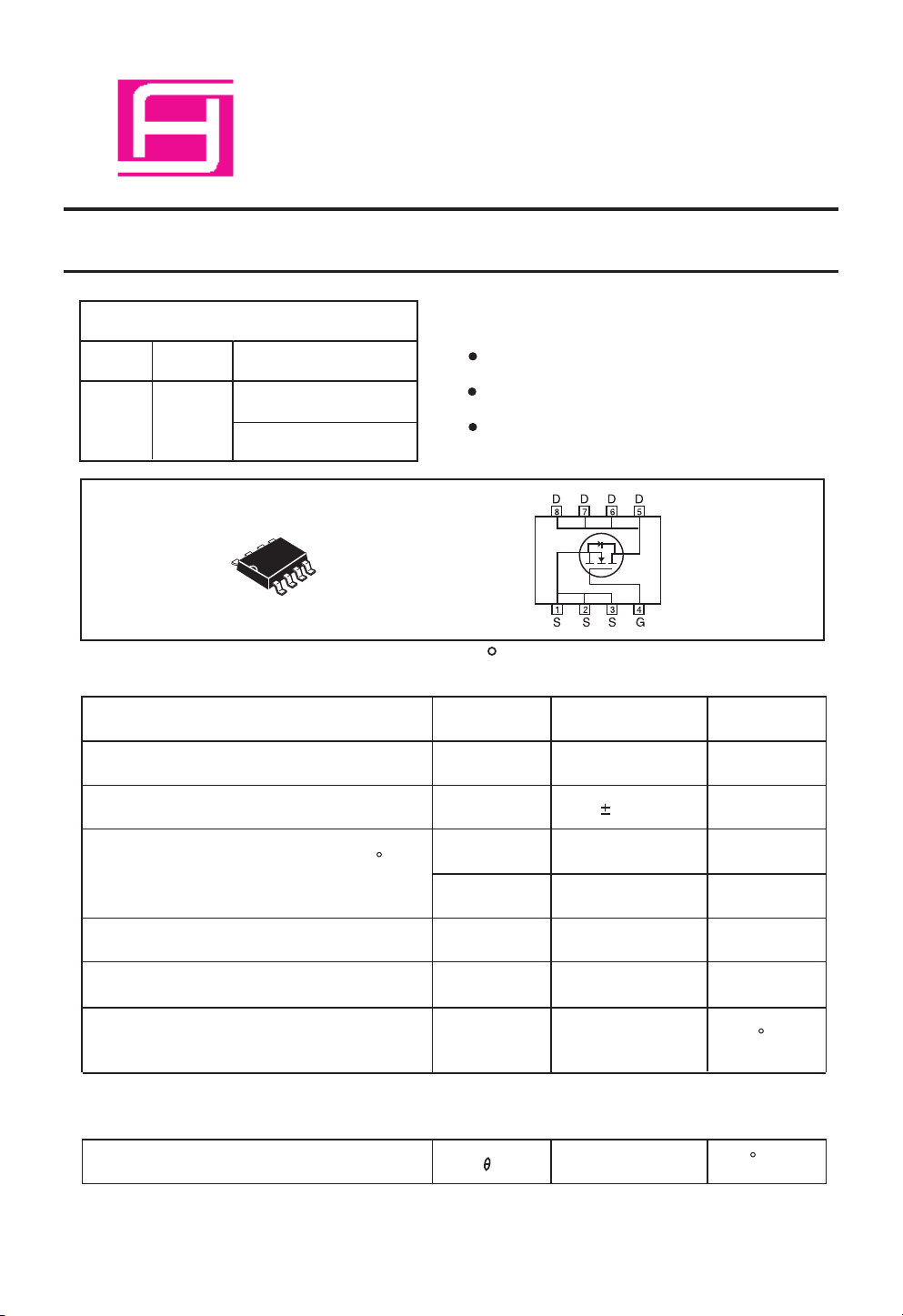
S O-8
W
) MAX
30 @ VG S = 10V
50 @ VG S = 4.5V
1
ABS OLUTE MAX IMUM R ATINGS (TA=25 C unless otherwise noted)
F E ATUR E S
S uper high dense cell des ign for low R
R ugged and relia ble.
S urface Mount P ackage.
P R E LIMINAR Y
DS (O N
).
P arameter
Drain-S ource Voltage
G ate-S ource Voltage
Drain C urrent-Continuous @ TJ=125 C
-P ulsed
Drain-S ource Diode F orward C urrent
Maximum P ower Dissipa tion
a
b
(300ms P uls e Width)
a
a
Operating J unction and S torage
Temperature R ange
THE R MAL C HAR AC TE R IS TICS
Thermal R esistance, J unction-to-Ambient
S ymbol
V
DS
V
G S
I
D
I
DM
I
S
P
D
TJ, T
S TG
a
R
J A
Limit Unit
30
20
7
28
2.8
2.5
-55 to 150
50
V
V
A
A
A
W
C
C
/W
1
Page 2
S DM9410
E LE C T R IC AL C HAR AC T E R IS TIC S (T A 25 C unles s otherwis e noted)
P arameter
S ymbol
=
C ondition
Min
Typ
OF F C HAR AC TE R IS TIC S
Drain-S ource Breakdown Voltage
Zero G ate Voltage Drain Current
G ate-Body Leakage
ON C HAR ACT E R IS TIC S
b
G ate Threshold Voltage
Drain-S ource On-S tate R es is tance
On-S tate Drain C urrent
0V, ID 250uA
B V
DS S
I
DS S
I
G S S
V
G S (th)
R
DS (ON)
I
D(ON)
g
F S
c
VDS 24V, V
V
G S
V
DS VG S
V
G S
V
G S
V
DS
V
DS
=
=
= =
=
=
=
=
= 5V, V
= =
G S
20V, VDS 0V
, ID = 250uA
=
10V, I
D
4.5V,I
D
=
G S
5V, I
D
0V
=
7A
3.5A
= 10V
7A
30
1
30
1.8
12
V
G S
DYNAMIC C HAR AC TE R IS TIC S
C
Max
1
100
3
30
50
Unit
V
uA
nA
V
m ohm
m ohm
A
SF orward Transconducta nce
Input C apacitance
Output C apacitance
R evers e Trans fer C apa citance
S WIT C HING CHAR AC TE R IS TIC S
Turn-On Delay Time
R ise Time
Turn-Off Delay T ime
F all Time
Total G a te C harge
G ate-S ource Charge
G ate-Drain Charge
C
IS S
V
DS
=15V, V
C
OS S
C
R S S
c
t
D(ON)
t
r
t
D(OFF )
t
f
f =1.0MH
VDD = 15V,
ID = 1A,
V
G S
= 10V,
R
G E N
VDS =15V, ID =1A,V
Q
g
VDS =15V, ID =1A,V
Q
Q
gs
gd
VDS =15V, ID = 1A,
V
G S
=10V
2
= 10
Z
G S
ohm
= 0V
G S
G S
=10V
=4.5V
510
235
56
21
20
27
115
13
6.5
2
2.3
230
40
40
55
20
10
P
F
P
F
P
F
ns
ns
ns
ns
nC
nC
nC
nC
Page 3
S DM9410
E LE C T R IC AL C H AR AC T E R IS TIC S (TA=25 C unless otherwise noted)
P arameter
S ymbol
C ondition
Min
Typ
C
Max
Unit
DR AIN-S OU R C E DIO DE C HAR AC T E R IS T IC S
Diode F orward Voltage
Notes
a.S urface Mounted on F R 4 B oard, t 10s ec.
b.Pulse Test:P ulse W idth 300us, Duty Cycle 2%.
c.G uaranteed by des ign, not s ubject to production testing.
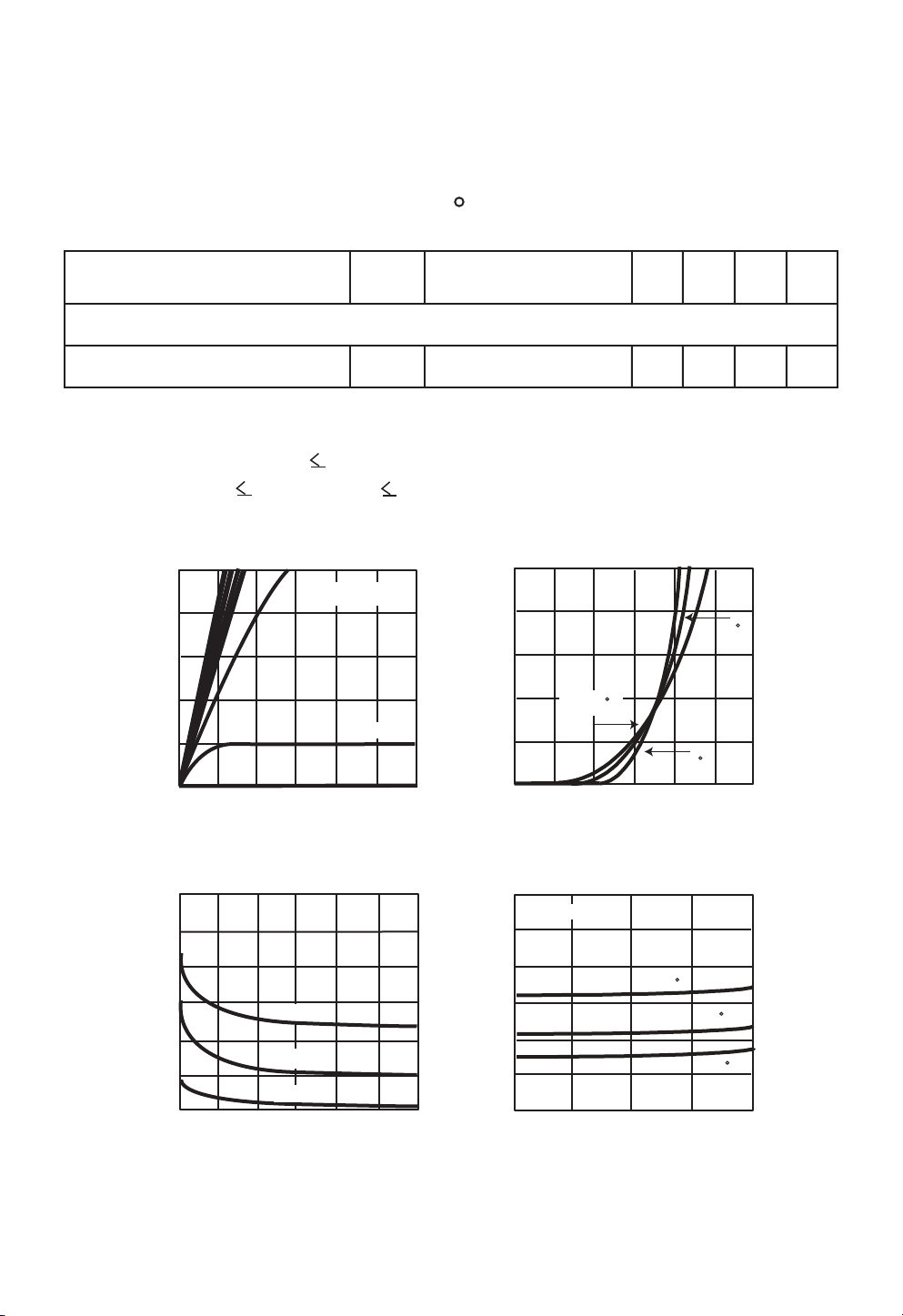
25
VGS=10, 9,8, 7,6,5,4 V
20
15
10
5
ID, Drain C urrent(A)
0
0 0. 5 1 1. 5 2 2 .5 3
VDS , Drain-to-Source Voltage (V)
F igure 1. Output Chara cteris tics
V
VGS =3V
S D
b
V
G S
= 0V, Is =5.3A
25
20
15
10
5
ID, Dra in C urrent (A)
0
0. 0 1. 0 2. 0 3. 0 4.0 5. 0 6.0
0.76
T j=1 25 C
-55 C
VGS , G ate-to-S ource Voltage (V )
1.1
25 C
F igure 2. Tra nsfer Characteris tics
V
120 0
100 0
800
600
400
C , C apa cita nce (pF)
200
0
0 5 1 0 15 2 0 25 30
VDS , Drain-to S ource Voltage (V)
C iss
C oss
C rss
F igure 3. C apacitance
On-R esistance(O hms)
R DS (O N),
0. 030
0. 025
0. 020
0. 015
0. 010
0. 005
VGS =10V
T j=1 25 C
0
0 5 10 1 5 20
ID, Dra in C urrent(A)
F igure 4. On-R es ista nce Va riation with
Drain C urrent and Temperature
3
25 C
-55 C
Page 4
S DM9410
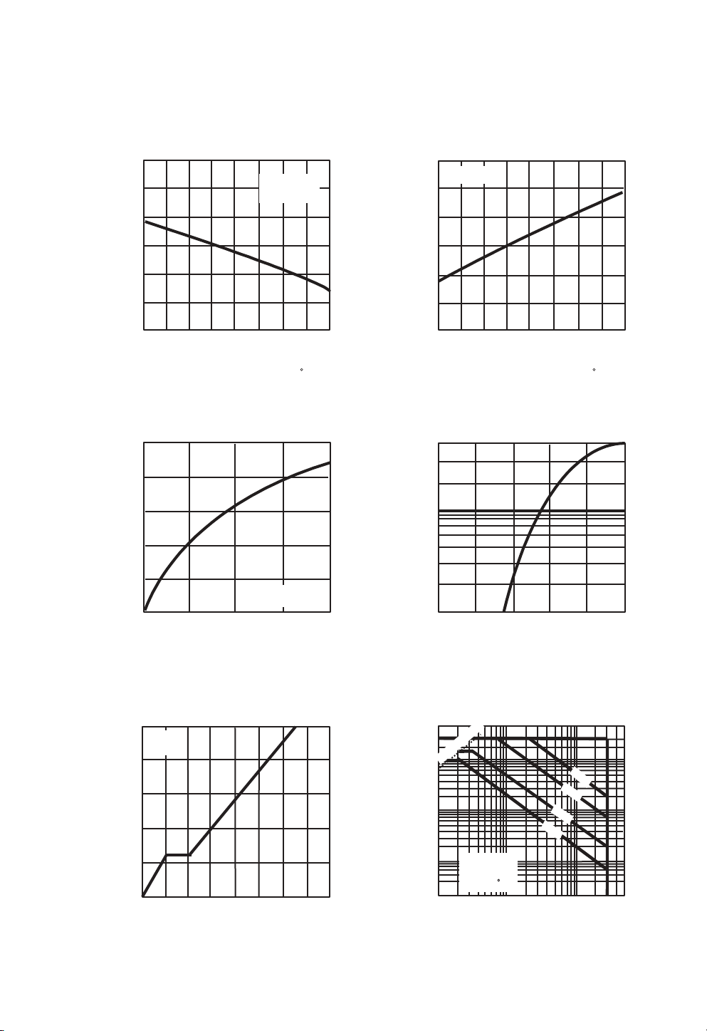
1.09
1.06
1.03
1.00
0.97
Vth, Normalized
0.94
0.91
G ate-S ource T hreshold Volta ge
-50 -25 0 25 50 75 100 125 150
VDS=V
ID=250uA
Tj, J unction T emperature ( C )
F igure 5. G ate Threshold V ariation
with Temperature
25
20
15
10
1.15
G S
B VD SS , Normalized
Dra in-S ource Breakdown Volta ge
ID=-250uA
1.10
1.05
1.00
0.95
0.90
0.85
-50 -25 0 25 50 75 100 125 150
Tj, J unction T emperature ( C )
F igure 6. B reakdown Volta ge Varia tion
with Temperature
40. 0
10. 0
5
gFS , T rans conductance ( S )
0
0 5 10 15 20
VDS=15V
IDS , Dra in-S ource C urrent (A)
F igure 7. T ransconductance V ariation
with Dra in C urrent
10
VDS=15V
ID=1A
8
6
4
2
VGS , Gate to S ource V oltage (V )
0
0 2 4 6 8 10 12 14 16
Qg, T ota l G ate C harge (nC )
F igure 9. G ate Charge
4
Is , S ource-drain current ( A)
1.0
0.4 0. 6 0.8 1. 0 1.2 1.4
VSD , Body Diode Forward Voltage (V )
F igure 8. B ody Diode F orward V oltage
Varia tion with S ource C urrent
40
10
1
0.1
ID, Dra in C urrent (A )
0.03
t
mi
Li
ON )
(
S
D
R
1
0
m
s
1
0
0
ms
1
V
G S
=10V
1s
DC
S ingle Pulse
TA=25 C
0.1 1 10 30 50
VDS , Drain-S ource V oltage ( V)
F igure 10. Maximum S afe
Ope rating Area
Page 5

S DM9410
DD
V
on
t
d(off)
t
r
t
90%
10% 10%
INVE R TE D
50% 50%
V
V
d(on)
t
OU T
IN
10%
R
IN
V
V
G S
G EN
R
G
L
D
OU T
V
S
P ULS E W IDT H
90%
t
off
f
t
90%
F igure 11. S witching T est C ircuit
2
1
Duty C yc le=0.5
0. 2
0. 1
0. 1
0. 05
0. 01
0. 02
S ingle P ulse
-4
10
-3
10
r(t), Normalized E ffe ctive
T rans ient Thermal Impeda nce
F igure 13. Normalized T herma l T rans ient Impedance Curve
F igure 12. S witching W aveforms
-2
10
S quare Wave P ulse D uration (sec)
-1
10
DM
P
1
t
2
t
1. R qJA (t)=r (t) * R qJA
2. R qJA=S ee Data shee t
3. TJ M-T A = PDM* R qJA ( t)
4. Duty C ycle , D=t1/t2
1 10 100
5
 Loading...