

Page 1
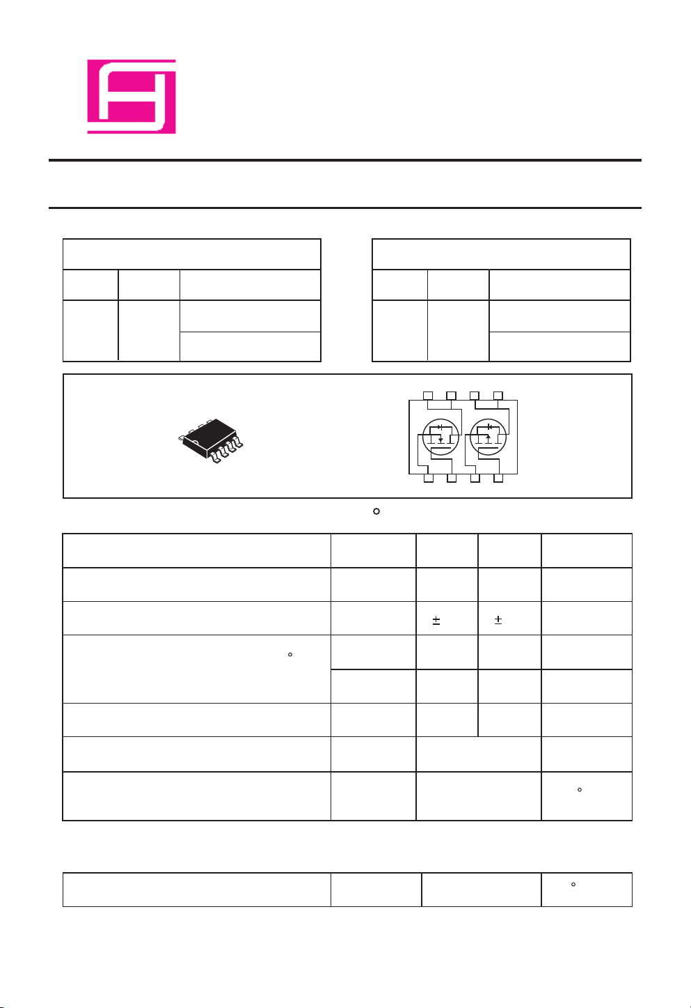
S DM8958
S amHop Microelec tronics C orp.
P R E LIMINAR Y
Dual E nhancement Mode Field E ffect T ransistor ( N and P C hannel)
PR ODUC T S UMMAR Y
VDS S
30V
ID
7A
S O-8
(N-C hannel)
R DS (O N) ( m
32 @ VGS = 10V
50 @ VGS = 4.5V
1
PR ODUC T S UMMAR Y
W
)
MAX
VDS S
-30V
ID
-5A
D1 D1 D2 D2
8 7 6 5
1 2 3 4
S 1 G 1 S 2 G 2
ABS OLUT E MAX IMUM R ATINGS (TA=25 C unles s otherwise noted)
(P -C ha nnel)
R DS (O N) ( m
52 @ VGS = -10V
90 @ VGS = -5V
W
)
MAX
P arameter
Drain-S ource Voltage
G ate-S ource Voltage
Drain C urrent-C ontinuous @ TJ=125 C
-P uls ed
Drain-S ource Diode F orward C urrent
Maximum P ower Dis s ipation
a
b
a
a
Opera ting J unction and S torage
Temperature R ange
THE R MAL C HAR AC TE R IS TIC S
Thermal R es is tance, J unction-to-Ambient
S ymbol
V
DS
V
G S
I
D
I
DM
I
S
P
D
TJ, T
S TG
a
R
qJ A
N-C ha nnel
30
20
7.0
28
1.7
-55 to 150
P -C hannel
-30
20
-5.0
-20
-1.7
2.0
62.5
Unit
V
V
A
A
A
W
C
C
/W
1
Page 2
S DM8958
N-C hannel E LE C TR IC AL C HAR AC T E R IS TIC S (TA 25 C unles s otherwise noted)
P arameter
S ymbol
C ondition
=
Min
Typ
C
Max
Unit
OF F C HAR AC TE R IS TIC S
Drain-S ource Breakdown Voltage
Zero G ate Voltage Drain C urrent
G ate-Body Leakage
ON C HAR AC T E R IS TIC S
b
G ate T hres hold Voltage
Drain-S ource On-S tate R es is tance
On-S tate Drain C urrent
0V, ID 250uA
B V
DS S
I
DS S
I
G S S
V
G S (th)
R
DS (ON)
I
D(ON)
g
F S
c
VDS 24V, V
V
G S
V
DS VG S
V
G S
V
G S
V
DS
V
DS
=
=
= =
=
=
=
=
= 5V, V
= =
G S
20V, VDS 0V
, ID = 250uA
10V, I
D
=
4.5V,I
D
=
G S
5V, I
D
6.0A
0V
=
6.0A
5.0A
= 10V
30
1 1.8
30
16
1
100
3
32
50
V
uA
nA
V
m ohm
m ohm
A
SF orward Trans conductance
V
G S
DYNAMIC C HAR AC T E R IS TIC S
Input C apacitance
Output C apacitance
R evers e Transfer C apacitance
S WIT C HING C HAR AC TE R IS T IC S
Turn-O n Delay Time
R ise Time
Turn-O ff Delay Time
F a ll Time
Total G ate C harge
G ate-S ource C harge
G ate-Drain C harge
P
C
IS S
V
DS
=15V, V
C
OS S
C
R S S
c
t
D(ON)
t
r
t
D(OFF)
t
f
f =1.0MH
VDD = 15V,
ID = 1A,
V
G E N
RL = 15 W
R
G E N
VDS =15V, ID = 1A,V
Q
g
VDS =15V, ID = 1A,V
Q
Q
gs
gd
VDS =15V, ID = 1A,
V
G S
=10V
2
Z
= 10V,
= 10 W
G S
= 0V
G S
G S
=10V
=4.5V
510
235
56
40 ns
21
20 40
27
55
115 230
13
20
10
6
2.1
2
F
P
F
P
F
ns
ns
ns
nC
nC
nC
nC
Page 3
S DM8958
P-Channel E LE C TR ICAL C HAR AC TE R IS TICS (TA 25 C unless otherwise noted)
P arameter
S ymbol
=
C ondition
Min
Typ
C
OF F C HAR AC TE R IS TIC S
Drain-S ource Breakdown Voltage
Zero G ate Voltage Drain C urrent
G ate-Body Leakage
ON C HAR AC T E R IS TIC S
b
G ate T hres hold Voltage
Drain-S ource On-S tate R es is tance
On-S tate Drain C urrent
0V, ID -250uA
B V
DS S
I
DS S
I
G S S
V
G S (th)
R
DS (ON)
I
D(ON)
g
F S
c
VDS -24V, V
V
G S
V
DS VG S
V
G S
V
G S
V
DS
V
DS
=
=
= =
=
=
=
=
= -5V, V
= =
G S
20V, VDS 0V
, ID = -250uA
=
-10V, I
D
-5V , I
D
=
G S
-5V, I
D
0V
=
-4.5A
-4A
= -10V
- 4.5A
-30
-1 -1.7 -3
-20
10
V
G S
DYNAMIC C HAR AC T E R IS TIC S
Max
-1
100
52
90
Unit
V
uA
nA
V
m ohm
m ohm
A
SF orward Trans conductance
Input C apacitance
Output C apacitance
R evers e Transfer C apacitance
S WIT C HING C HAR AC TE R IS T IC S
Turn-O n Delay Time
R ise Time
Turn-O ff Delay Time
F a ll Time
Total G ate C harge
G ate-S ource C harge
G ate-Drain C harge
c
C
IS S
C
OS S
C
R S S
t
D(ON)
t
t
D(OFF)
t
Q
Q
Q
V
f =1.0MH
VD = -15V,
r
RL = 15
ID = -1A,
V
f
R
VDS=-15V,ID=-5.3A,V
g
VDS=-15V,ID=-5.3A,V
gs
gd
VDS =-15V, ID = - 5.3A,
V
3
DS
=-15V, V
G E N
= -10V,
G E N
= 10
G S
=-10V
W
P
P
P
ns
ns
ns
nC
nC
nC
nC
F
F
F
860
G S
= 0V
Z
470
180
20 ns
9
10 40
37
90
W
G S
=-10V
G S
=-4.5V
23 110
15
20
8.7
10.5
3
4
Page 4

S DM8958
E LE C T R IC AL C HAR AC T E R IS TIC S (TA=25 C unles s otherwise noted)
P arameter
S ymbol
C ondition
Min
Typ
C
Max
Unit
DR AIN-S OUR C E DIO DE C HAR AC T E R IS T IC S
Diode F orwa rd Voltage
V
Notes
a.S urface Mounted on F R 4 Board, t 10sec.
b.Puls e Test:P ulse W idth 300us, Duty C ycle 2%.
< <
<
c.G uaranteed by design, not subject to production testing.
N-C hannel
25
VGS=10, 9,8, 7,6,5, 4V
20
15
10
5
ID, Drain Current(A)
0
0 0. 5 1 1. 5 2 2 .5 3
VDS , Drain-to-S ource Voltage (V)
F igure 1. Output C haracteris tics
VGS =3V
S D
V
V
b
G S
= 0V, Is =1. 7A N-C h 0. 77
G S
= 0V, Is =-1.7A P -C h
25
20
15
10
5
ID, Dra in C urrent ( A)
0
0. 0 1.0 2. 0 3. 0 4 .0 5. 0 6.0
T j=12 5 C
-55 C
VGS , G ate-to-S ource Volta ge (V )
F igure 2. Trans fer C hara cteristics
-0.82
25 C
1. 2
-1.2
V
120 0
100 0
800
600
400
C , C apa citance (pF )
200
0
0 5 10 1 5 2 0 25 30
VDS , Drain-to S ource Voltage ( V)
C iss
C oss
C rss
F igure 3. Capa citance
On-R esistanc e(Ohms)
R DS (O N),
0. 030
0. 025
0. 020
0. 015
0. 010
0. 005
VGS =10V
T j=12 5 C
0
0 5 10 15 2 0
ID, Dra in C urrent(A)
F igure 4. On-R esistance Variation with
Drain C urrent and Temperature
4
25 C
-55 C
Page 5

N-C hannel
S DM8958
1.09
1.06
1.03
1.00
0.97
Vth, N ormalized
0.94
0.91
G ate-S ource T hreshold Voltage
-50 -25 0 25 50 75 100 125 150
Tj, Junction T emperature ( C )
VDS=V
ID=250
F igure 5. Gate T hreshold V ariation
with Temperature
25
20
15
10
1.15
ID=-250
G S
uA
1.10
1.05
1.00
0.95
0.90
B VDS S, Normalized
0.85
Dra in-S ource B rea kdown V oltage
-50 -25 0 25 50 75 1 00 1 25 150
uA
Tj, Junction T emperature ( C )
F igure 6. Brea kdown Voltage Variation
with Temperature
40. 0
10. 0
5
gFS , T ransconductance (S )
0
0 5 10 15 20
IDS , Drain-S ource C urrent (A)
with Dra in C urrent
VDS=15V
Is , S ource-drain current ( A)
1.0
0.4 0.6 0.8 1.0 1.2 1.4
VS D, Body Diode F orward Voltage (V)
F igure 8. Body Diode F orward V oltage
Variation with S ource C urrent
5
Page 6

P -C hannel
S DM8958
25
20
-V GS =10, 9,8, 7,6, 5V
15
10
5
-ID , Drain Current (A )
0
0 0. 5 1.0 1. 5 2. 0 2. 5 3.0
-V DS , D rain-to-S ource Voltage (V )
F igure 1. Output C haracteris tics
300 0
250 0
200 0
20
-55 C
16
4V
3V
12
8
4
-ID , Drain Current (A )
0
0 0 .5 1 1. 5 2 2.5 3
25 C
T j=12 5 C
5
-V GS , Ga te-to-S ource Voltage (V )
F igure 2. Trans fer C hara cteristics
1. 8
VGS =-10V
ID=-5.3A
1. 6
1. 4
150 0
100 0
C , C apa citance (pF )
500
0
0 5 10 15 20 25 30
-V DS , D rain-to S ource Voltage (V)
F igure 3. Capa citance
C iss
C oss
C rss
1. 2
1. 0
On-R esistanc e(Ohms)
(Normalized)
0. 8
R DS (O N),
0. 6
-50 0 5 0 100 150
Tj, Junction T emperature ( C )
F igure 4. On-R esistance Va riation with
Temperature
6
Page 7

P -C hannel
S DM8958
1.09
VDS=V
1.06
1.03
1.00
0.97
Vth, N ormalized
0.94
G ate-S ource T hreshold Voltage
0.91
-50 -25 0 25 50 75 100 125 150
G S
ID=-250uA
Tj, Junction T emperature ( C )
F igure 5. Gate T hreshold V ariation
with Temperature
15
12
1.15
ID=-250uA
1.10
1.05
1.00
0.95
0.90
B VDS S, Normalized
0.85
Dra in-S ource B rea kdown V oltage
-50 -25 0 25 50 75 1 00 1 25 150
Tj, Junction T emperature ( C )
F igure 6. Brea kdown Voltage Variation
with Temperature
20. 0
V
G S
=0V
10. 0
9
6
3
gFS , T ransconductance (S )
0
0 5 10 15 20
-ID S, D rain-S ource C urrent (A)
VDS=-15V
F igure 7. Trans conductance V ariation
with Dra in C urrent
-Is , S ource-drain current (A )
1.0
0.4 0.6 0.7 0.9 1.1 1.3
-V S D, B ody D iode Forward V oltage (V)
F igure 8. Body Diode F orward V oltage
Variation with S ource C urrent
7
Page 8

S DM8958
N-C hannel
10
VDS=15V
8
ID=9A
6
4
2
VGS , G ate to S ource V oltage (V )
0
0 2 4 6 8 10 12 14 16
Qg, Total G ate C harge (nC)
F igure 9. Gate C harge
P -C hannel
10
VDS=-15V
8
ID=-4. 5A
6
4
40
ON ) L imit
(
DS
R
10
1
1
V
G S
0.1
ID, Dra in C urrent (A )
0.03
=10V
S ingle P ulse
TA=25 C
10ms
100
ms
1s
DC
0.1 1 10 30 50
VDS , Drain-S ource Voltage ( V)
F igure 10. Ma ximum S afe
Operating A rea
50
10
imit
L
ON )
(
S
D
R
1
10
m
s
10
0m
s
1s
D
C
2
VGS , G ate to S ource V oltage (V )
0
0 3 6 9 12 15 18 21 24
Qg, Total G ate C harge (nC)
F igure 9. Gate C harge
V
G S
0.1
-ID , D rain C urrent ( A)
0.03
=-10V
S ingle P ulse
TA=25 C
0.1 1 10 30 50
-V DS , Dra in-S ource Volta ge (V )
F igure 10. Ma ximum S afe
Operating Area
8
Page 9

S DM8958
DD
V
on
t
d(off)
t
r
d(on)
R
IN
V
V
G S
G EN
R
G
L
D
OU T
V
S
t
OU T
V
IN
V
10%
t
90%
10% 10%
INVE R T E D
50% 50%
P ULS E W IDT H
90%
t
off
f
t
90%
F igure 11. S witching Tes t Circuit
2
1
Duty C yc le=0.5
0. 2
0. 1
0. 1
0. 05
0. 01
0. 02
S ingle P ulse
-4
10
-3
10
r(t), Norma lized E ffec tive
T rans ient Thermal Impedance
F igure 13. Normalized Therma l Trans ient Impedance C urve
F igure 12. S witching Waveforms
-2
10
S quare W ave P ulse Dura tion (s ec)
-1
10
DM
P
1
t
2
t
1. R θJA (t)=r (t) * R θJA
2. R θJA=S ee Data shee t
3. TJ M-T A = PDM* R θJA ( t)
4. Duty C ycle , D=t1/t2
1 10 100
9
 Loading...