

Page 1
S DM8401
S amHop Microelec tronics C orp.
Augus t , 2002
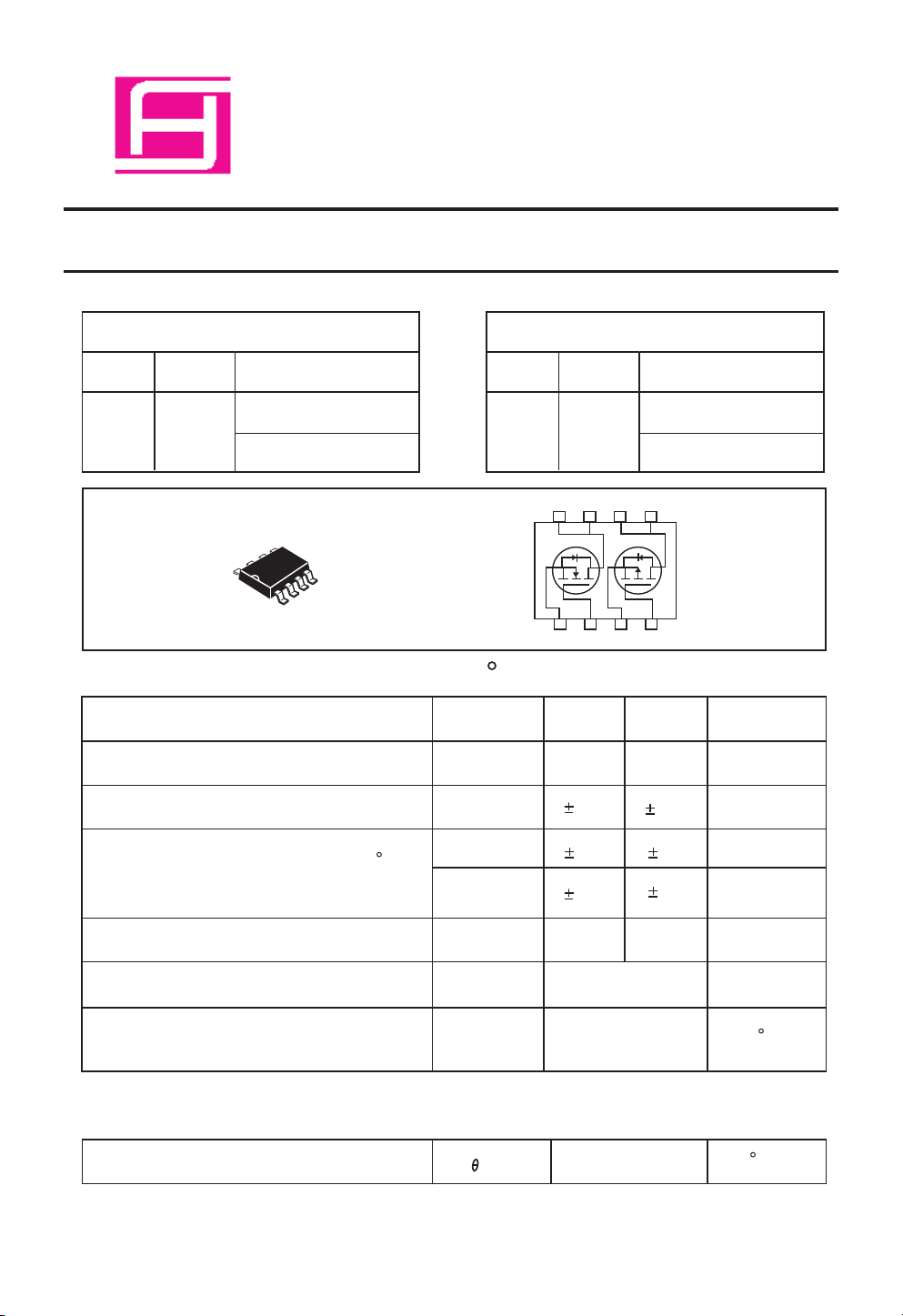
Dual E nhancement Mode Field E ffect T ransistor ( N and P C hannel)
PR ODUC T S UMMAR Y
VDS S
30V
ID
6A
S O-8
(N-C hannel)
R
DS (O N) ( m W ) T YP
18.5 @ VGS = 10V
25 @ VGS = 4.5V
1
PR ODUC T S UMMAR Y
VDS S
-30V
ID
-4.5A
D1 D1 D2 D2
8 7 6 5
1 2 3 4
S 1 G 1 S 2 G 2
ABS OLUT E MAX IMUM R ATINGS (TA=25 C unles s otherwise noted)
(P -C ha nnel)
R
DS (O N) ( m W ) T YP
38.5 @ VGS = -10V
57.5 @ VGS = -4.5V
P arameter
Drain-S ource Voltage
G ate-S ource Voltage
Drain C urrent-C ontinuous @ TJ=125 C
-P uls ed
Drain-S ource Diode F orward C urrent
Maximum P ower Dis s ipation
a
b
a
a
Opera ting J unction and S torage
Temperature R ange
THE R MAL C HAR AC TE R IS TIC S
Thermal R es is tance, J unction-to-Ambient
S ymbol
V
DS
V
G S
I
D
I
DM
I
S
P
D
TJ, T
S TG
a
R
J A
N-C ha nnel
30
20
6.0
18.0
1.7
-55 to 150
P -C hannel
-30
20
4.5
15
-1.7
2.0
62.5
Unit
V
V
A
A
A
W
C
C
/W
1
Page 2
S DM8401
N-C hannel E L E C TR ICAL CHAR AC TE R IS TICS (TA 25 C unles s otherwis e noted)
P arameter
5
OF F C HAR AC TE R IS TIC S
Drain-S ource Breakdown Voltage
Zero G ate Voltage Drain C urrent
G ate-Body Leakage
ON C HAR AC T E R IS TIC S
G ate T hres hold Voltage
Drain-S ource On-S tate R es is tance
On-S tate Drain C urrent
S ymbol
B V
DS S
I
DS S
I
G S S
b
V
G S (th)
R
DS (ON)
I
D(ON)
g
F S
c
C ondition
V
G S
=
VDS 24V, V
V
G S
V
DS VG S
=
V
G S
V
G S
V
DS
V
DS
=
0V, ID 250uA
=
G S
= =
=
=
10V, I
4.5V, I
=
= 10V, V
= =
10V, I
0V
16V, VDS 0V
, ID = 250uA
=
D
9A
D
7A
=
G S
= 10V
D
20A
=
Typ
Min
30
1.5
1 3
18.5
25
40
16
C
Max
21
DYNAMIC C HAR AC T E R IS TIC S
1
100
32
Unit
V
uA
nA
V
m ohm
m ohm
A
SF orward Trans conductance
Input C apacitance
Output C apacitance
R evers e Transfer C apacitance
S WIT C HING C HAR AC TE R IS T IC S
Turn-O n Delay Time
R ise Time
Turn-O ff Delay Time
F a ll Time
Total G ate C harge
G ate-S ource C harge
G ate-Drain C harge
C
IS S
V
DS
=15V, V
G S
= 0V
C
OS S
C
R S S
c
t
D(ON)
t
r
t
D(OFF)
t
f
Q
g
Q
gs
Q
gd
f =1.0MH
Z
VDD = 15V,
ID = 1A,
V
G S
= 10V,
R
G E N
= 6
VDS =15V, ID =9A,V
VDS =15V, ID =9A,V
VDS =15V, ID = 9A,
V
G S
=10V
2
G S
=10V
G S
=4.5V
950
420
110
7
30
14
54
25.2
14.612.1
5.12
4.8
35
P
F
P
F
P
F
ns
ns
ns
ns
nC
nC
nC
nC
Page 3

S DM8401
P-Channel E L E C TR ICAL C HAR ACTE R IS TICS (TA 25 C unles s otherwis e noted)
P arameter
S ymbol
=
C ondition
Min
Typ
C
Max
Unit
OF F C HAR AC TE R IS TIC S
Drain-S ource Breakdown Voltage
Zero G ate Voltage Drain C urrent
G ate-Body Leakage
ON C HAR AC T E R IS TIC S
b
G ate T hres hold Voltage
Drain-S ource On-S tate R es is tance
On-S tate Drain C urrent
0V, ID -250uA
B V
DS S
I
DS S
I
G S S
V
G S (th)
R
DS (ON)
I
D(ON)
g
F S
c
VDS -24V, V
V
G S
V
DS VG S
V
GS
V
GS
V
DS
V
DS
=
=
= =
=
=
=
=
= -5V, V
= =
G S
20V, VDS 0V
, ID = -250uA
=
-10V, I
D
-4.5V, I
D
=
G S
-15V, I
D
0V
=
-4.5A
-3.6A
= -10V
- 4.5A
-30
-1 -1.5 -3
-20
38.5
57.5
105
-1
100
53
95
V
m A
nA
V
m ohm
m ohm
A
SF orward Trans conductance
V
G S
DYNAMIC C HAR AC T E R IS TIC S
Input C apacitance
Output C apacitance
R evers e Transfer C apacitance
S WIT C HING C HAR AC TE R IS T IC S
Turn-O n Delay Time
R ise Time
Turn-O ff Delay Time
F a ll Time
Total G ate C harge
G ate-S ource C harge
G ate-Drain C harge
c
C
IS S
C
OS S
C
R S S
t
D(ON)
t
t
D(OFF)
t
Q
Q
Q
V
f =1.0MH
VD = -15V,
r
RL = 15
ID = -1A,
V
f
R
VDS=-15V,ID=-4.9A,V
g
VDS=-15V, ID=-4.9A,V
gs
gd
VDS =-15V, ID = - 4.9A,
V
3
DS
=-15V, V
G E N
= -10V,
G E N
= 6
G S
=-10V
P
P
P
ns
ns
ns
nC
nC
nC
nC
F
F
F
860
G S
= 0V
Z
457
140
20 ns
9
10 40
37
90
23 110
G S
=-10V
G S
=-4.5V
15
8
20
10
3
4
Page 4

S DM8401
E L E C T R IC A L C HA R A C TE R IS TIC S (TA=25 C unles s otherwis e noted)
C
Typ
P ar ameter
S ymbol
C ondition
Min
Max
Unit
DR AIN-S OUR C E DIODE C HAR AC T E R IS T IC S
Diode F orwa rd Voltage
V
Notes
a.S urface Mounted on F R 4 Board, t 10sec.
b.Puls e Test:P ulse W idth 300μs, Duty C ycle 2% .
< <
<
c.G uaranteed by design, not subject to production testing.
N-C hannel
25
VGS =10, 9,8, 7,6,5, V
20
15
10
VGS =4V
5
ID, Drain Current(A)
0
0 0. 5 1 1. 5 2 2 .5 3
VDS , Drain-to-S ource Voltage (V)
F igure 1. O utput C har acteristics
S D
V
V
b
G S
= 0V, Is =1. 7A N-C h 0. 77
G S
= 0V, Is =-1.7A P -C h
25
20
15
10
5
ID, Dra in C urrent ( A)
0
0. 0 1.0 2. 0 3. 0 4 .0 5.0 6.0
T j=12 5 C
VGS , G ate-to-S ource Volta ge (V )
F igure 2. Tr ansfer C haracteristics
-55 C
-0.80
25 C
1. 2
-1.2
V
5
300 0
250 0
200 0
150 0
100 0
C , C apa citance (pF )
500
0
0 5 10 1 5 20 25 30
VDS , Drain-to S ource Voltage ( V)
C iss
C oss
C rss
F igure 3. C apacitance
4
On-R esistanc e(Ohms)
R DS (O N),
0. 030
0. 025
0. 020
0. 015
0. 010
0. 005
VGS =10V
T j=12 5 C
25 C
-55 C
0
0 5 10 1 5 20
ID, Dra in C urrent(A)
F igure 4. O n-R esistance Var iation with
Dr ain C urrent and Temper ature
Page 5

N-C hannel
S DM8401
1.09
5
1.06
1.03
1.00
0.97
Vth, N ormalized
0.94
0.91
G ate-S ource T hreshold Voltage
-50 -25 0 25 50 75 100 125 150
Tj, Junction T emperature ( C )
VDS=V
ID=250
GS
uA
F igur e 5. G ate T hr eshold V ar iation
with T emperatur e
25
20
15
10
1.15
ID=-250
1.10
1.05
1.00
0.95
0.90
B VDS S, Normalized
0.85
Dra in-S ource B rea kdown V oltage
-50 -25 0 25 50 75 1 00 1 25 150
uA
Tj, Junction T emperature ( C )
F igur e 6. B reakdown V oltage V ar iation
with T emperatur e
40. 0
10. 0
5
gFS , T ransconductance (S )
0
0 5 10 15 20
IDS , Drain-S ource C urrent (A)
with Dr ain C ur r ent
VDS=15V
Is , S ource-drain current ( A)
1.0
0.4 0.6 0.8 1.0 1.2 1.4
VS D, Body Diode F orward Voltage (V)
F igur e 8. B ody Diode Forwar d V oltage
V ariation with Sour ce C ur rent
5
Page 6

S DM8401
P-C hannel
25
-V GS =10, 9,8, 7V
20
15
10
5
-ID , Drain Current (A )
0
0 0. 5 1.0 1. 5 2. 0 2. 5 3.0
-V DS , D rain-to-S ource Voltage (V )
6V
5V
4V
3V
20
-55 C
16
12
8
4
-ID , Drain Current (A )
0
0 0 .5 1 1. 5 2 2.5 3
25 C
T j=12 5 C
-V GS , Ga te-to-S ource Voltage (V )
F igure 1. O utput C har acteristics F igure 2. T r ansfer C haracteristics
150 0
125 0
100 0
750
500
C , C apa citance (pF )
250
0
0 5 10 15 20 25 30
-V DS , D rain-to S ource Voltage (V)
F igure 3. C apacitance
C iss
C oss
C rss
1. 8
VGS =-10V
ID=-4.9A
1. 6
1. 4
1. 2
1. 0
On-R esistanc e(Ohms)
(Normalized)
0. 8
R DS (O N),
0. 6
-50 0 5 0 100 150
Tj, Junction T emperature ( C )
F igure 4. O n-R esistance Var iation with
Temper ature
6
Page 7

P-C hannel
S DM8401
1.09
VDS=V
1.06
1.03
1.00
0.97
Vth, N ormalized
0.94
G ate-S ource T hreshold Voltage
0.91
-50 -25 0 25 50 75 100 125 150
GS
ID=-250
uA
Tj, Junction T emperature ( C )
F igur e 5. G ate T hr eshold V ar iation
with T emperatur e
15
12
9
6
1.15
1.10
1.05
1.00
0.95
0.90
B VDS S, Normalized
0.85
Dra in-S ource B rea kdown V oltage
ID=250μA
-25 0 25 50 75 1 00 125 150
Tj, Junction T emperature ( C )
5
F igur e 6. B reakdown V oltage V ar iation
with T emperatur e
20. 0
10. 0
VGS=0V
3
gFS , T ransconductance (S )
0
0 5 10 15 20
-ID S, D rain-S ource C urrent (A)
VDS=-15V
F igur e 7. T ransconductance V ar iation
with Dr ain C ur r ent
-Is , S ource-drain current (A )
1.0
0.4 0.6 0.8 1.0 1.2 1.4
-V S D, B ody D iode Forward V oltage (V)
F igur e 8. B ody Diode Forwar d V oltage
V ariation with Sour ce C ur rent
7
Page 8

S DM8401
N-C hannel
10
VDS=15V
5
8
ID=9A
6
4
2
VGS , G ate to S ource V oltage (V )
0
0 4 8 12 16 20 24 28 32
Qg, Total G ate C harge (nC)
F igur e 9. G ate C harge
40
10
0.1
ID, Dra in C urrent (A )
0.03
mit
) L i
(O N
DS
R
1
1
V
G S
=10V
S ingle P ulse
TA=25 C
0.1 1 10 30 50
VDS , Drain-S ource Voltage ( V)
F igur e 10. M aximum Safe
10ms
100 ms
1s
DC
Oper ating Area
P-C hannel
10
VDS=-15V
8
ID=-4.5A
6
4
50
DS
R
(O N) L im
it
10ms
100 ms
1s
DC
10
1
1
2
VGS , G ate to S ource V oltage (V )
0
0 3 6 9 12 15 18 21 24
Qg, Total G ate C harge (nC)
F igur e 9. G ate C harge
8
0.1
-ID , D rain C urrent ( A)
0.03
V
G S
=-10V
S ingle P ulse
TA=25 C
0.1 1 10 50
-V DS , Body D iode Forward V oltage (V)
F igur e 10. M aximum Safe
Oper ating Area
Page 9

S DM8401
DD
V
on
t
d(off)
t
r
d(on)
R
IN
V
V
G S
G EN
R
G
L
D
OU T
V
S
t
OU T
V
IN
V
10%
t
90%
10% 10%
INVE R T E D
50% 50%
P ULS E W IDT H
90%
t
off
f
t
90%
5
F igur e 11. Switching T est C ir cuit
2
1
Duty C yc le=0.5
0. 2
0. 1
0. 1
0. 05
0. 01
0. 02
S ingle P ulse
-4
10
-3
10
r(t), Norma lized E ffec tive
T rans ient Thermal Impedance
F igur e 13. Normalized T hermal T r ansient I mpedance C urve
F igur e 12. Switching W aveforms
-2
10
S quare W ave P ulse Dura tion (s ec)
-1
10
DM
P
1
t
2
t
1. R θJA (t)=r (t) * R θJA
2. R θJA=S ee Data shee t
3. TJ M-T A = PDM* R θJA ( t)
4. Duty C ycle , D=t1/t2
1 10 100
9
 Loading...